Non-Volatile Memory (NVM) Subsystem
Feature list
Storage of CPU code and data in several program NVM (P-NVM) banks:
- Independent read access to the banks
- Read-while-write capability between the banks
Storage of EEPROM data in dedicated data NVM (D-NVM) banks:
- High write endurance
- Read-while-write capability versus the code P-NVM banks
- Security code and data can be stored in separate banks (depends on specific device configuration) with possible access protection to the security CPU
- Infineon configuration block storage (ICB) for microcontroller configuration data and NVM configuration, firmware
- User configuration block storage (UCB) for microcontroller configuration data and configuration settings which can be changed by the application software
- Boot ROM for microcontroller start-up software (SSW)
Functional description
The non-volatile memory (NVM) subsystem consists of a data memory unit (DMU), program flash interface (PFI), and the non-volatile memory component. The NVM component comprises the program flash (PFLASH) memories, data flash (DFLASH) memories, flash standard interface (FSI) modules, and a program flash read write buffer (PFRWB).
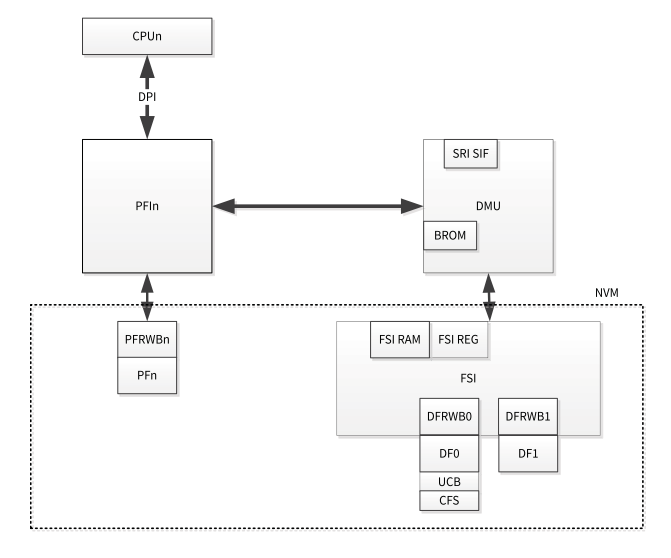
The data memory unit (DMU) controls command sequences executed on all program and data flash memories. The Flash Standard Interface (FSI) executes erase, program and verify operations on all flash memories. The program flash (PFLASH) is divided into one or more banks, each connected to a CPU. It is used by the application to store program code and data constants. Compute performance is optimized by using a point-to-point interface to minimize latency and maximize bandwidth. Each PFLASH is connected to a PFlash Read/Write Buffer (PFRWB) that performs the ECC correction and detection and provides the read data to the system.
Each PFLASH bank has a unique point-to-point fast connection to a CPU provided by a program flash interface (PFI). The PFI interfaces between the CPU and the PFRWB and contain Prefetch Buffers for storing speculative data. The data flash (DFLASH) module is used to emulate EEPROM and store data and is divided into two banks. The DFlash Read Write Buffer (DFRWB) of the FSI interfaces to the DFLASH provide the read data. The Data Flash module also contains regions to store configuration data - the user configuration blocks (UCBs). The Boot ROM (BROM) is connected to the system via the DMU SRI port. The tuning protection (commonly called the "Secure Watchdog") protects user software and user data from maltuning data.
The aim of the PFLASH NVM system is to store program code and data constants, and the implementation of Erase Counters. The purpose of the DFLASH NVM is the emulation of Electrically Erasable Programmable Read Only Memory (EEPROM)for user applications (CPU-EEPROM) and security applications (HSM-EEPROM). User Configuration Blocks (UCB) are used for password-based read protection combined with write protection, as well as for read-only UCB configured with unique chip identifier and trimming data.
The configuration Sector (CFS) stores system set-up data, which is not accessible by the user. Data stored in the NVM is protected by ECC checksum. An ECC decoder at the output of the NVM corrects and detects faults in the NVM array. The NVM is fault tolerant and supports system operation in the presence of a number of NVM bit errors. For Program Flash the calculation of the ECC checksum is extended across the address to provide read protection against addressing faults. If the Flash is not operating in the application, the NVM may be programmed and erased by command sequences executed by the FSI micro controller. All read accesses to Flash are memory mapped reads. Margin read levels may be used to check how completely a cell is programmed or erased. The Non-Volatile Memory interface micro architecture also includes a security layer and a safety layer.
The Security Layer is provided by the DMU and PFI modules. Read protection is enabled/disabled globally for the whole Flash Module. Write protection is enabled/disabled with a Flash Module sector-based granularity. The Safety Layer allows a master-specific read access protection to each Flash Module (Bank). The master specific read and write access controls individual Special Function Registers (SFRs). Integrity of data stored in the NVM is ensured by an ECC checksum. And the integrity of PFlash read path is ensured by monitoring of read parameters in the FSI (MISR, redundant Flip Flops, etc.), by PFI partial lockstep mechanism, protection of PFlash wait cycles with ECC checksum, by protection of data from PFI to CPU by ECC checksum and an additional safety mechanism to ensures, the local PFlash is not being programmed/erased when not expected by PFI.