High Speed Serial Link (HSSL)
The HSSL module provides point-to-point communication of both single data values and of large data blocks, called streams. The communicating partner can be complex microcontrollers, or a microcontroller and a device with only basic execution capabilities.
The HSSL module supports single block 8, 16, or 32-bit data write or read transfers either to or from the target device's register. Using a streaming channel, it also supports transfers of long 256-bit data blocks.
The HSSL module consists of two main sub-modules:
- High Speed Serial Link (HSSL)
- High Speed Communication Tunnel (HSCT)
The HSSL sub-module implements Transport Layer tasks and hands over the data to the HSCT sub-module which provides Data Link Layer and Physical Layer services, data serialization, and transmission. All transfers are protected by safety features such as Cyclic Redundancy Check (CRC) and timeout.
Feature list
Flexible functional configuration by application software
- Frame formatting configuration
- TX-link baud-rate support (10 MHz/20 MHz SysClk(System Clock)): 5 MBaud (low speed) and 320 MBaud (high speed)
- TX-link baud-rate support (25 MHz SysClk): 6.25 MBaud (low speed) and 320 MBaud (high speed)
- RX-link baud-rate support (20 MHz SysClk): 5 MBaud (low speed), 20 MBaud (medium speed) and 320 MBaud (high speed)
- RX-link baud-rate support (10 MHz SysClk): 5 MBaud (low speed) and 320 MBaud (high speed)
- RX-link baud-rate support (25 MHz SysClk): 6.25 MBaud (low speed) and 320 MBaud (high speed
Transmit HSSL frames to external devices and handle all protocol relevant topics
- Writing a single 8, 16, or 32-bit data value into the register of a target device
- Supports transfers of a long 256-bit streaming data block
- Automatic frame transfer ID (IDentity) generation for detection of dropped frames
- Acknowledge for command and stream frames
Receive HSSL frames from external devices and handle all protocol relevant topics
- Reading single data from an 8, 16, or 32-bit register of a target device
- Supports reception of a long 256-bit streaming data block
- Transfers protected by CRC16 (16-bit Cyclic Redundancy Check)
- Support of 32-bit address range
Read and write HSSL frame data either to or from system address space
- Support of Direct Memory Access (DMA) driven multiple register write or read transfers
- Two stage FIFOs (First in, First Outs) for transmitting and receiving streaming data
Flexible event signaling and interrupt structure
- Programmable timeouts for detection of blocked answer transfers
- Remote trigger of an event or an interrupt in the target device by the initiator
- Total 17 interrupt lines, four types of channel specific interrupt per channel and one module interrupt
- Automatic FIFO flush when entering the run mode, for error handling
- Read and write access protection by an external Memory Protection Unit (MPU)
- Identification of the target by the JTAG ID (Joint Test Action Group Identification) number
- Multi-slave connection supports up to three slaves
- The communication interface is based on IEEE 1596.3 LVDS IOs (Low Voltage differential Signaling Input Outputs) and provides driver swing amplitude configuration restricted
Functional description
The block diagram of the HSSL module is shown in Figure 1.
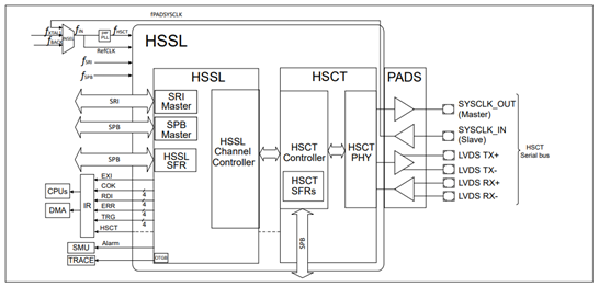
The HSSL has one alarm, called 'HSSL SRI Read Data EDC Error' interfacing to the SMU (EDC stands for Error Detection and Correction). A set of 17 interrupts are mapped to IR (Interrupt Router), four types of channel specific interrupts per channel and one module interrupt. In order to support the debugging activities, the HSSL provides a set of internal signals to the on-chip debug system OCDS (On Chip Debug System) through OTGB (OnChip Trigger Generation Bus) trigger buses.
High Speed Serial Link (HSSL)
The HSSL sub-module provides point-to-point communication for both single data values and large data blocks, called streams. The functionality of each of these channels is further sub divided as 'transmitter and receiver' and 'Initiator and target' controllers by the HSSL channel controller. The communicating devices can be complex micro controllers, or a microcontroller and a device with only basic execution capabilities. There are four channels to transfer single values to/from target. They support direct writing of 8/16/32 bit data from the initiator into a target’s local address map (e.g., registers and memory), as well as reading a value from a target, performed by a modules internal SPB/SRI bus master on the target side. For transferring large data blocks there is a channel containing FIFOs. The HSSL module implements transport layer tasks and hands over the data to another module which provides data link layer and physical layer services, data serialization and transmission. All transfers are protected by safety features like CRC and timeout. The SRI and SPB master interface on the target HSSL helps in accessing the peripherals on the corresponding bus. The SPB slave interface helps in accessing the special function registers of HSSL.
The SRI master interface is capable of performing both single and burst reads and writes on the SRI bus. The SPB slave interface is used by an SPB master (DMA, CPU, HSSL SPB Master) for writing the HSSL SFRs, so configuring the module and performing single read and write operations.
High Speed Communication Tunnel (HSCT)
The lower layer companion module and logic control the lower communication layers positioned between two devices, the data, and the physical layer. They consist of the High-Speed Communication Tunnel (HSCT) and pads.
The chip-to-chip interface employs a digital interface for inter chip communication between a master or a slave HSCT instance. The interface is capable of running in a master or in a slave HSCT mode. During configuration phase the role of the Interface (master or slave) has to be defined. It is not intended to change the system role after initialization and start-up. The HSCT controller consists of framer, de-framer and the corresponding FSMs (finite state machines) along with the SFRs controlled via SPB slave interface.
The interface consists of a full-duplex RX and TX high-speed data interface based on double ended differential signals (in total 4 lines) and a master clock interface (SYSCLK_OUT). The master IC owns the crystal and provides the clock to the slave. The interface reset is derived from the System reset and provided by chip internal reset signaling.