Clocking (CLOCK)
The clocking system is responsible for providing all clocks that are necessary for microcontroller operation. This is valid for all functional, test, and debug modes. It also provides clocks for external applications that can be selected from internal sources.
The main functional blocks of this cluster are:
Clocking: The clocking system is functionally divided into two major clock domains:
- System clock domain for clocks covering central processing units, interconnect and data transfers structures, non-volatile memories, timers, debug, trace, and the core functions of the communication interfaces
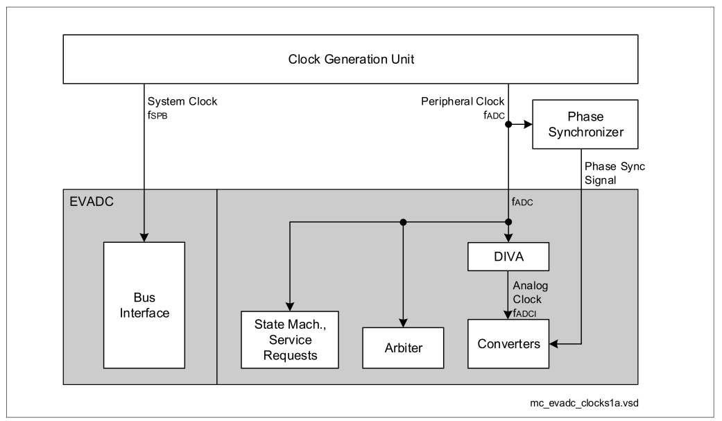
- Peripheral clock domain for the protocol related parts of the communication interfaces and analog digital converters
Each domain has a master clock which is used to derive the related sub-clocks by programmable division and clock gating. System clocks are synchronous to each other, and peripheral clocks are asynchronous to each other and to the system clocks. Selected clocks can be routed to external outputs for debug, test, and further processing.
Feature list
- Physical SoC interface for externally provided clocks (crystal oscillator (XTAL OSC) or HSSL system clock (SYSCLK))
- Internally generated back-up clock provided by an embedded voltage regulator (EVR) oscillator for independent operation in the absence of a crystal clock
- Internally generated linear ramp clock to support power-up and power-down, reset, and emergency operation with low supply voltage drops and low current peaks
- Up-scaling of externally supplied clocks up to a maximum frequency of fPLL0, phase locked loops (System PLL)
- Peripheral PLL supports three outputs of 160 MHz, 200 MHz, and 200 MHz
- System clock domain with frequency modulation to reduce electromagnetic interference (EMI)
- Peripheral clock domain with low jitter and low noise to comply with jitter and the signal-to-noise ratio requirements of selected communication protocols and analog to digital converters (ADC)
- Peripheral clock domain with frequency modulation for optional use to reduce EMI
- Low skew distribution of all system clocks to enable global synchronous operation within the microcontroller unit (MCU)
- Independent generation and distribution of all system and peripheral clocks
- Software programming interface for clock configuration and status observation
- Clock monitoring to support ASIL D safety protection and security
- Provision of selected internal system and peripheral clocks to physical outputs of the MCU
- Reset support functions (clock gating and frequency adaptation)
Functional description
The clock system is built up as a chain composed from different building blocks which allow different function parts for the complete chain. The building blocks as shown in the following figure are:
- Basic clock generation with internal and external oscillators (Clock Source)
- Clock speed up-scaling with phase locked-loops (PLL)
- Clock distribution with clock control units (CCU)
- Individual clock configuration within other functional blocks
The clocking system is composed of various functions which are physically spread over the clusters for timing, routing, and power consumption reasons. The starting point of clock generation is either an external crystal, ceramic resonator, or an external clock. These clock sources are fed into an actively controlled oscillator circuit which produces the main clock source. This clock source in turn drives the clock generation function (PLLs) which synthesizes higher frequency master clocks for the system and peripheral clock domains.
The master clocks are divided down and activated on a user configurable basis in the distribution function. The divided clocks are finally distributed to the system and peripheral components of the whole device. There are two internal backup clock oscillators which provide master clocks for the distribution function in case the PLL operation is not available or the master distribution clock frequency must be adapted. This is required during power-up and power-down, resets, re-configuration, or a failure of the PLL circuit.
One of the internal back-up clock oscillators can also produce a clock signal that can be continuously changed in frequency. This feature has been introduced to limit current jumps during power-up and power-down, application resets, and emergency switching. The other internal oscillator is static in frequency and is also used as a diverse clock for safety monitoring. Selected clocks can also be provided outside the device. In addition, there are several monitors to safeguard the clocking system functions for safety and security purposes. The clocking system has its own bus slave agent which is attached to the SPB peripheral interconnect of the microcontroller.