Local Memory Unit (LMU)
The Local Memory Unit is an SRI peripheral providing access to volatile memory resources. Its primary purpose is to provide up to 256 KB of local memory for general purpose usage. A product may contain multiple instances of the LMU. Refer to the system memory map for the configuration applicable to each product. Each instance of the LMU has its own set of configuration registers.
Data stored in the local memory is protected by ECC at all points within the LMU. Areas of local memory can be write protected by configuring up to sixteen address ranges using SFRs in the LMU. Each of these ranges can be sized in thirty-two byte increments and has its own, independent list of Master Tag IDs permitted write access. Read accesses are not protected.
Feature list
An overview of the features implemented in the LMU:
Up to 256 KiB of SRAM
- Organized as 64 bit words
- Support for byte, half word and word accesses as well as double-word and burst accesses
- Memory can be used as overlay memory
Protection of LMU SRAM contents
- Sixteen programmable address regions can be protected
- Each address range has a programmable list of bus masters permitted read or write access based on the Unique master Tag ID
Functional description
Local Memory (LMU SRAM)
The LMU SRAM can be used for code execution, data storage or overlay memory. The address range of the memory is defined in the system memory map. As well as being accessed via cached, the memory can be accessed via non-cached memory addresses. The memory implements memory integrity checking for error detection and correction. This means that the memory must be initialized before reads are attempted with the integrity checking enabled to avoid generating spurious data corruption errors. Initializing with the memory integrity, logic disabled allows the LMU SRAM to support initialization using word (32-bit) or smaller writes as well as 64-bit writes. If memory integrity checking is enabled, a read access which fails the integrity check will cause an error condition to be flagged to the initiated bus master. An ECC error will also be reported to the SMU. The SMU will use this signal for error indication and triggering of an NMI trap.
The LMU SRAM is internally organized as a 64-bit memory without the possibility of sub-word accesses. This means that any write access of less than 64-bits of data needs an internal Read-Modify-Write (iRMW) operation to correctly write the data and update the ECC data. This happens transparently to the rest of the system unless an uncorrected ECC error is detected during the read phase of the iRMW. This ECC error will be flagged to the SMU in the same way as a data ECC error occurring during a normal read. LMU SRAM performance will be the same as, or better than the performance of the embedded flash. This applies to both the initial latency of the first word returned and also the incremental latency for each word in the same cache line fetched. If the CPU access cannot be handled by the LMU SRAM (e.g. an attempt has been made to access RAM with the LMU clock disabled), an SRI bus error is reported by the LMU. This will, for example, cause a CPU to take a DSE trap if the access is from a CPU and a DMA access to terminate with an error condition.
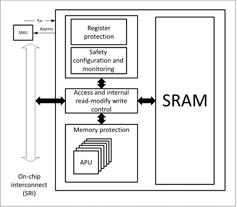
Memory Protection
The LMU allows the definition of sixteen protected regions of SRAM memory. The protection applies only to accesses to SRAM included in the LMU. The protection scheme is based on the use of Unique Master Tag IDs to identify the master attempting the access and allows for a six-bit tag individually identifying up to 64 masters.
After reset, the region address registers will be set to include the whole of the LMU SRAM address space and read and write access by all masters will be enabled. The registers implementing the memory protection scheme are protected by the “safety endinit” function. If overlapping regions are defined, then an access only needs to be permitted by one of the overlapping regions for it to succeed. When altering protection settings, it should be noted that, due to access pipelining in the LMU and resynchronization delays in the register block, an access to a memory address affected by the protection change occurring immediately after the register write initiating the change may, or may not, be affected by the changed settings. For the Cerberus and HSM masters, if present in the product, access protection only applies to write accesses. Read accesses from these masters are always successful.
LMU Register Protection
The LMU implements a standard register protection scheme for peripheral registers. This allows the control registers to be protected from write accesses by untrusted masters. Masters are identified using the SRI tag of the access and, if the appropriate bit is not set in the access enable registers, write accesses will be disconnected with error acknowledge.
Error Detection and Signaling
The LMU will detect several different classes of error which cannot necessarily be signaled on the SRI during the associated transaction. However, all errors will cause a trigger to be sent to the SMU for processing. Some will additionally cause a flag to be set in the MEMCON register. Examples of this include, if an ECC error occurs on the address phase of an SRI access an error will be signaled to the SMU. The SRI access will abort without attempting to modify RAM or SFR contents. If an ECC error occurs on the data phase of an SRI write access the error will also be signaled to the SMU. The write completes without signaling an SRI error. If an uncorrected ECC error is reported by the RAM during an SRAM read an error the signaling to the SMU will also be executed.
The hardware used to check and correct the read data from the SRAM is replicated and the output from the two instances is compared. In the event of a difference between the two outputs, an error condition will be signaled to the SMU. The second instance will use inverted logic to eliminate common failure modes. Internal registers used to transfer data between the RAM and the SRI interface are ECC protected. When detecting an error, it will be signaled to the SMU. If either the memory protection or register protection detects a protection violation, the violating access will be terminated with an error message or fails silently. In both cases, the error will be signaled to the SMU. The LMU will perform an internal Read-Modify-Write (iRMW) access when a write of less than 64-bits of data is performed. An ECC error reported by the RAM on the read phase will be signaled to the SMU.
The control logic of the LMU which is not suitable for protection by one of the ECC checks will be lockstepped (duplicated and compared). Any mismatch between the two copies of the logic will be detected and an alarm generated. The lockstep block also checks consistency of its own control state by maintaining all such information in redundant pairs of flip-flops where one flip-flop is the logical inverse of the other. Any of these pairs being in an inconsistent state will trigger a separate SMU alarm.
The hardware used to check and correct the read data from the SRAM is replicated and the data output from the two instances is compared. In the event of a difference between the two data outputs, an error condition will be signaled to the SMU. The second instance will use inverted logic to eliminate common failure modes. Internal registers used to transfer data between the RAM and the SRI interface are ECC protected. The LMU will also perform an internal Read-Modify-Write (iRMW) access when a write of less than 64-bits of data is performed. The LMU contains a clock control register, CLC, which allows the LMU to be put into a power saving mode.