Queued Synchronous Peripheral Interface (QSPI)
The main purpose of the QSPI module is to provide synchronous serial communication with external devices using clock, data-in, data-out and slave select signals. The focus of the module is set to fast and flexible communication: either point-to-point or master-to-many slaves communication. Parallel requests from on chip bus masters to a module will be executed sequentially via the on-chip bus system. Read-modify-write feature provides an atomic read/write sequence where no other master can access the module in between.
Feature list
This section describes the features of the QSPI module.
Master and slave mode operation
- Full-duplex operation
- Half-duplex operation
- Automatic slave select control
- Four-wire and three-wire type of connection
Flexible data format
- Programmable number of data bits: 2 to 32 data bits (plus parity: 3 to 33 bits)
- Programmable shift direction: LSB or MSB shift first
- Programmable clock polarity: Idle low or idle high state for the shift clock
- Programmable clock phase: data shift with leading or trailing edge of the shift clock
Baud rate generation
- Baud rates generated from high precision PLL clock, asynchronous to the system PLL
Interrupt generation
- On a transmitter FIFO event
- On a receiver FIFO event
- On an error condition (receive, baud rate, transmit error, parity error)
- On a phase transition (start of frame, end of frame ...)
- QSPI supports control and data handling by the DMA controller
- Flexible QSPI pin configuration
Hardware supported parity mode
- Odd/even/no parity
- Seven slave select inputs SLSIB...H in slave mode
Sixteen programmable slave select outputs SLSO[15:0] in master mode
- Automatic SLSO generation with programmable timing
- Programmable active level and enable control
- External de-multiplexing of the slave select outputs support
Several module reset options
- State machine reset per software (only the state machine)
- Module reset per software (both FIFOs, all registers and the state machine)
- Automatic stop option of the state machine in slave mode after baud rate error
- Loop-Back mode
- Interoperability with SSC and USIC modules of Infineon microcontroller families, and with popular (Q)SPI interfaces of multiple suppliers
Communication stop on RxFIFO full
- Shift register full and RxFIFO full can pause the communication
- Interrupt generation
High-speed input capture (HSIC)
- Provides input capture functionality for ADAS applications
- 15-bit counter with resolution of fPER
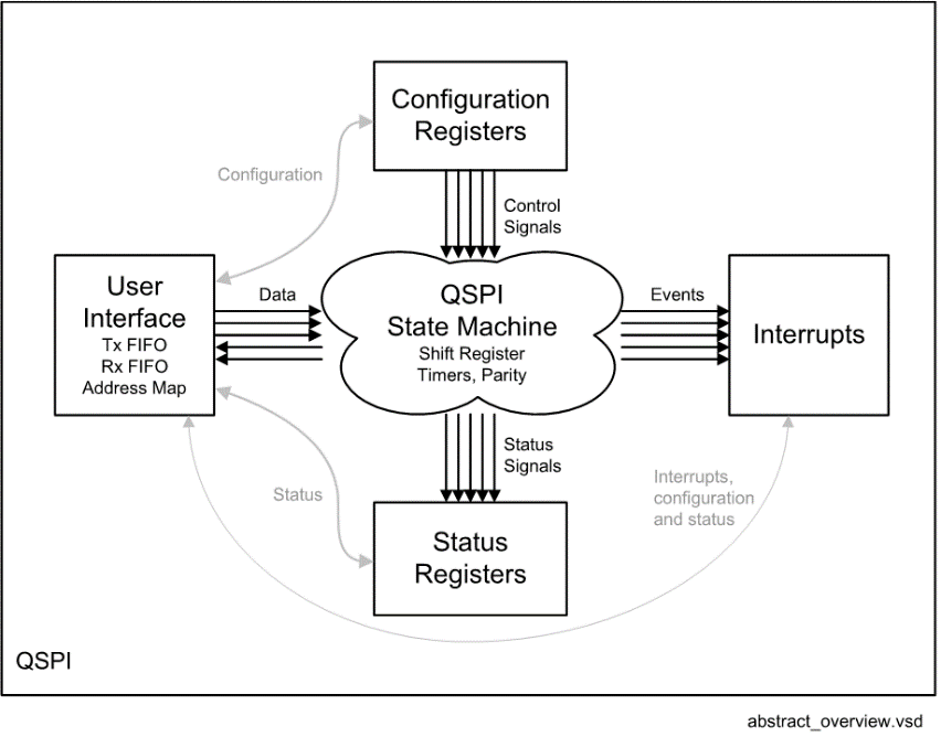
Abstract overview
An abstract overview of the QSPI module is shown in Figure 1. It shows the state machine with its configuration and status capabilities, the user interface, and the interrupts.
External signals
The communication between two devices using QSPI generally uses four signals: serial clock (SCLK), data in master to slave direction (MTSR: Master Transmit Slave Receive), data in slave to master direction (MRST: Master Receive Slave Transmit), and slave select signal (SLS).
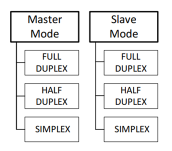
Operating modes
The QSPI operates in one of two modes regarding the generation of the serial clock and slave select signals - master or slave mode. The master generates and drives the clock and select signals, the slave receives these signals. The module operates in one of three modes regarding the direction of the communication and depending whether the transmission and the reception appear simultaneously or not - duplex, half-duplex and simplex mode. It gives six possible combinations for the operating mode of the QSPI: master duplex, half-duplex, and simplex, slave duplex, half-duplex, and simplex. The half-duplex mode can be implemented either by short-cut connection between two different pins on the PCB, one data output and one data input pin, or by using single pins mapped to both data input and data output signals (Figure 2)
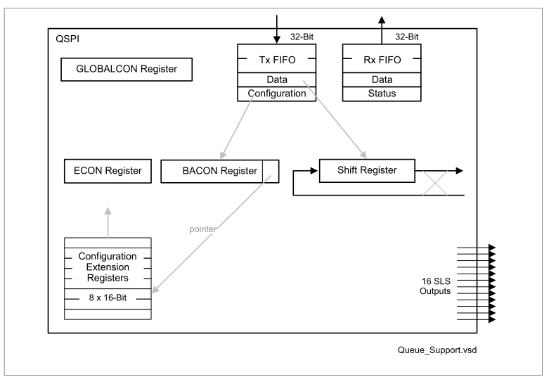
Queue support overview
The term “Queue Support” is used in this context to describe the functionality implemented for comfortable switching of the timing configuration of the QSPI frames, depending on the slave select signal which is to be activated. The main feature of the module is the possibility to take both the configuration and data to the TXFIFO, and to track down which TXFIFO entry is configuration, and which data. The QSPI module expects 32 basic configuration bits to be moved with one move (for example DMA move) from some on-chip general purpose RAM to the TXFIFO. These 32 configuration bits from the TXFIFO and the configuration bits from the eight configuration extension registers ECONz (z=0-7) z contained in the QSPI module, define together the full configuration of the module (Figure 3)
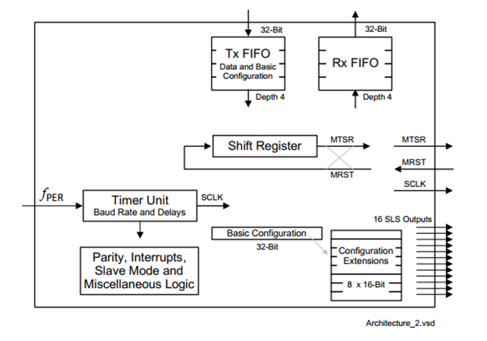
Architecture overview
Figure 4 shows the main blocks of the QSPI module. The TxFIFO and RxFIFO provide the user interface. The Shift Register and the “Miscellaneous Logic” block build the state machine of the module. The “Configuration Extensions” block provides comprehensive capabilities for configuring the QSPI frames.