Enhanced Delta-Sigma Analog-to-Digital Converter (EDSADC)
The enhanced delta-sigma analog-to-digital converter module (EDSADC) provides a series of analog input channels connected to on-chip modulators using the delta/sigma (DS) conversion principle. Digital input channels accept data streams from external modulators.
The on-chip demodulator channels convert these inputs to discrete digital values. The number of inputs and EDSADC channels depends on the chosen product type. Each converter channel can operate independently of the others, controlled by a dedicated set of registers. The results of each channel can be stored in a dedicated channel-specific result register. The on-chip filter stages generate digital results from the selected modulator signal. The EDSADC accepts data from different types of external modulators. Their data streams can be fed through selectable input pins. Also, on-chip modulators are available that accept differential or single-ended input signals.
Feature list
The following features describe the functionality of a DS converter:
Switched-capacitance input structure
- Input voltage range 0-5 V
- Common mode voltage: VAREF/x (x = 2, 4, 8), connection selectable for each pin
- Programmable gain (1:1/1:2/1:4)
- DC Offset < 5mVDC, gain error < ±0.2% (calibrated, on product level)
- Equivalent input impedance 500 kΩ typ. (for gain = 1, fMOD = 26.67 MHz)
On-chip modulator, single-bit second-order feed-forward modulator, sample frequency 16-40 MHz
Options to connect external standard DS modulators
- Selectable data stream inputs
- Selectable DS clock input or output
Demodulator (concatenated hardware filter stages)
- Configurable CIC filter with decimation rates of 4-512
- (Optional) Overshoot compensation filter
- FIR filter with 8 coefficients (10-bit) with decimation rate 2 (FIR0)
- FIR filter with 28 coefficients (10-bit) with decimation rate 1 or 2 (FIR1)
- Pass Band 0.723 to 100 kHz, output sampling rate fd = 2.17 to 300 kHz (decim. rate FIR1 = 2:1), Pass Band 0.723 to 10 kHz, output sampling rate fd = 4.34 to 60 kHz (decim. rate FIR1 = 1:1), Pass band ripple: dfd < ±1%
- Stop band attenuation: 0.5 to 1 × fd: >40 dB/1 to 1.5 × fd: >45 dB/1.5 to 2 × fd: > 50 dB/2 to 2.5 × fd: >55 dB/2.5 to OSR/2 × fd: > 60 dB
- Limit checking support
Optional high-pass filter for DC compensation (f -3dB = 10-5 × fd), configurable
- Hardware offset/gain calibration and compensation
- Parallel auxiliary CIC filter with limit checking for alarm generation
Support for resolver applications
- Carrier signal generator (differential sine output)
- Signal evaluation including rectification, delay compensation and carrier elimination
Automatic limit checking
- Two-level boundary comparator
- Separate indication signals
Functional description
The delta-sigma analog to digital converter module provides several channels providing an on-chip modulator with an associated demodulator including a configurable filter chain for demodulation, decimation, and filtering.
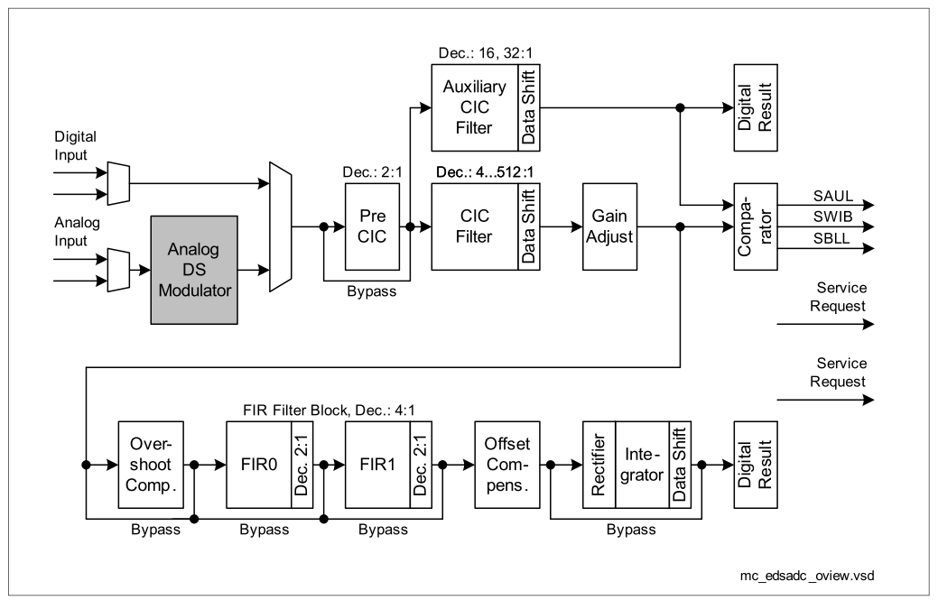
The EDSADC is connected to other on-chip modules to support functions on system level. The on-chip single-bit second-order feed-forward modulator converts an analog input signal to a datastream. Several types of external modulators can be connected to the input path. The modulator clock signal can be generated internally or can be fed from an external clock source. The digital filter chain (see figure below) builds the demodulator which produces result values at a configurable output rate. The elements of the filter chain can be activated according to the requirements of the application. The filter chain configuration determines the attenuation and delay properties of the filter. The decimation at a configurable rate reduces the modulator’s input sampling rate to a lower result data rate that is suitable for the application.
The CIC filter provides the basic filtering and decimation with a selectable decimation rate. Two FIR filters, each with a decimation rate of 2 (also 1 for FIR1), allow effective signal shaping by attenuating the upper frequencies of the signal spectrum. The high-pass filter provides offset compensation by removing the DC component of the input signal. The integrator accumulates a configurable amount of result values. The number of samples is programmable by software or can be controlled by a hardware signal.
Functionality of the integrator:
- Further reduction of the data output rate for the application
- Calculation of average values with selectable start point, for example, for shunt current measurement applications
- Support for resolver applications to get the baseband signal for the motor position calculation
Each channel can generate service requests to trigger DMA transfers or to request CPU service. Offset calibration and gain calibration are done in hardware. The calibration values are determined automatically by a hardware algorithm. This can be triggered initially after a reset or repeatedly during operation.
The on-chip carrier signal generator produces a selectable output signal (sine, triangle, rectangle) which can be used to drive a resolver. Synchronization of each input signal to the carrier signal ensures correct integration of the resolver input signals. The basic module clock is the peripheral clock signal fADC.
A comparator supports limit checking, for example, for overcurrent detection. Two limit values can be defined to restrict the generation of service requests to result values within a configurable area. This saves CPU performance and/or DMA bandwidth while continuously monitoring the input signal.