AN0012 SPU input and output DMA
TriCore™ TC3xx AURIX™ family
About this document
Scope and purpose
The second generation AURIX™ offers enormous computing power and fast responsive real-time behavior. It also supports low-, mid-, and high-end Radar applications. To ensure the fastest signal processing capabilities a high-performance signal processing unit (SPU) is integrated.
This document describes the input and output direct access memory (DMA) mechanism of the SPU using second generation AURIX™.
This application note is applicable for all second generation AURIX™ devices with at least one SPU instance available. (
TC39x
,
TC35x
,
TC33x
).
Intended audience
This document is intended for design engineers, technicians, and developers of electronic systems with basic knowledge of radar processing and the SPU.
Overview
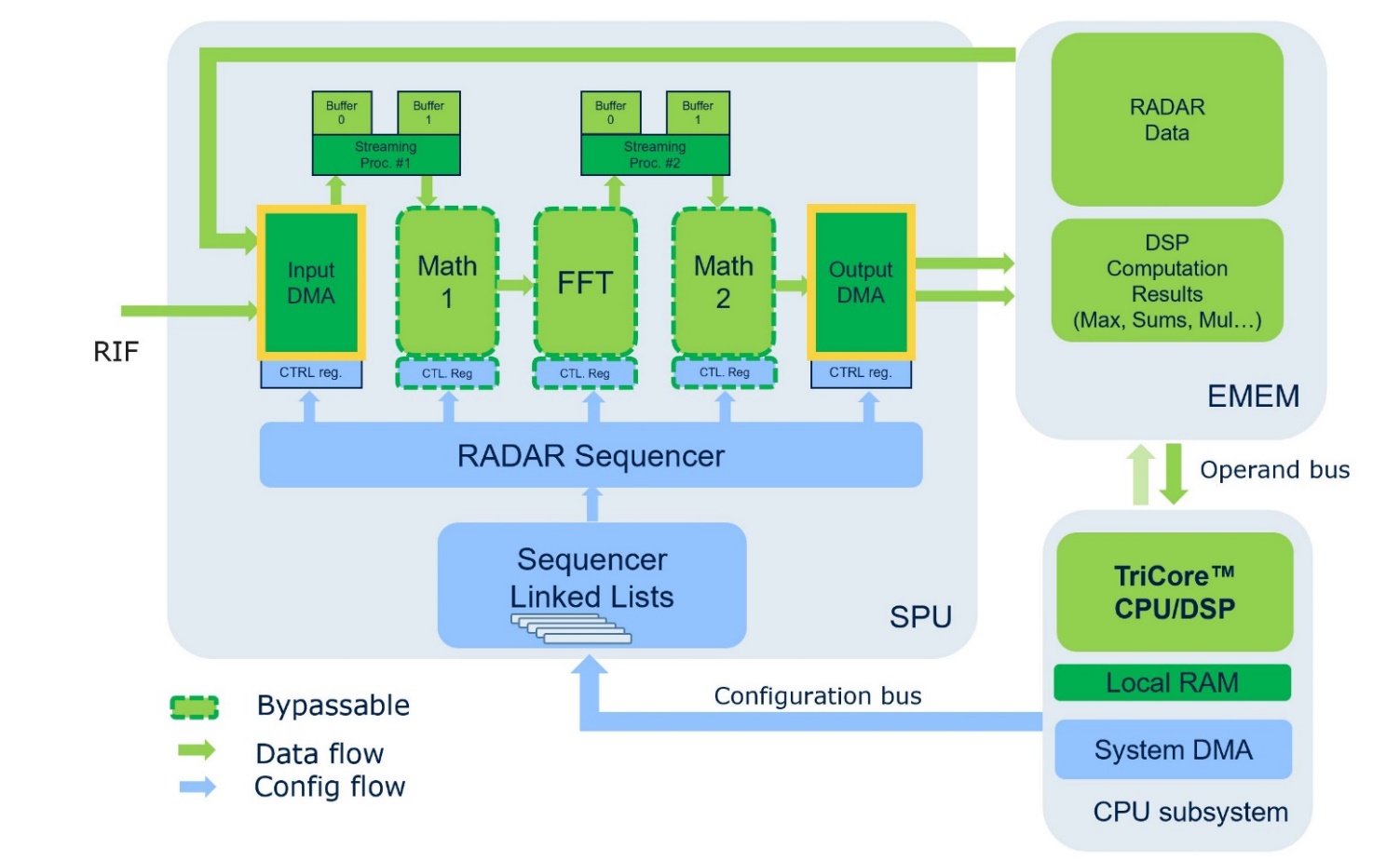
Input and output DMA in the signal processing unit (SPU) subsystem
shows input and output DMA (marked in yellow) in the SPU subsystem. The input DMA engine can either passively accept data pushed by the analog-digital-converter (ADC) interfaces (RIF or Radar Interface) or actively load data of an existing data cube from the Radar Memory also referred to as Extension Memory (EMEM). The task of the input DMA is to structure data in the buffer memory for subsequent processing in the SPU pipeline. Thus, the input DMA has to make sure that all data required to perform the configured processing steps is fed into the processing pipeline at a time. Examples where a complete data set is required include:
Fast Fourier Transforms (FFT):
All data points to perform the FFT need to be available
Integration of results across multiple antennas:
Data points from all antennas need to be available
The output DMA engine is used to write results to Radar Memory (EMEM).
Figure 1. Input DMA and output DMA in the SPU system
Working principles of input DMA
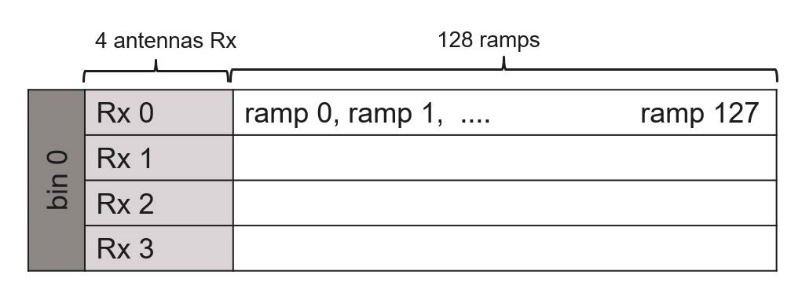
Depiction of radar data in Radar Memory
In radar applications data can often be ordered in three dimensions: multiple samples taken along a frequency sweep, multiple subsequent frequency sweeps (ramps), and data recorded by multiple antennas. To account for these three dimensions of data in Radar Memory, the schematic shown in
Figure 2
is used to represent the flat 1D data array stored in Radar Memory. The two left columns are used as indices for – depending on context – antenna, ramp or sample index.
For better understanding concrete values are depicted while these can be adapted to each dedicated use case. The values used are summarized in
Table 1
.
Parameter | Symbol | Value |
|---|---|---|
Number of samples per ramp | 1024 | |
Number of antennae | 4 | |
Number of ramps | 128 | |
Number of range bins after 1 st FFT | 512 |
Figure 2. Structure of radar data in Radar Memory
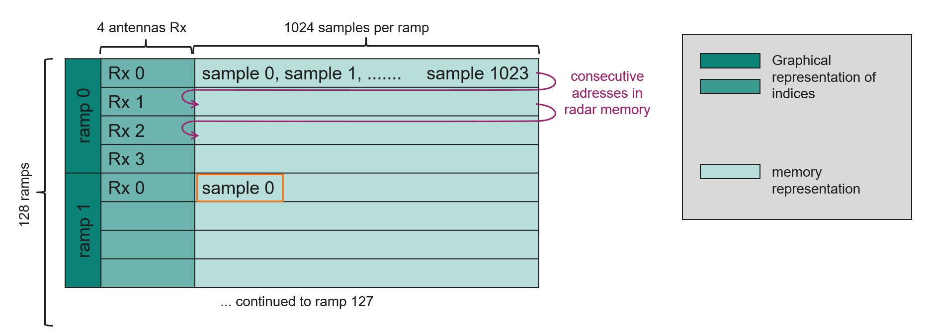
Note: The marked memory location (orange square) corresponds to (ramp 1-antenna 0-sample 0).
Using EMEM input
The input DMA operates either with the RIF or the Radar Memory (EMEM) as data source (compare
Figure 1
). This section describes the use of EMEM data as input.
The input DMA engine is designed to perform data transfers from Radar Memory to the SPU processing pipeline using address offsets from a configurable base address. Data is read from Radar Memory in 256-bit words and the input DMA can read 256 bits of data every two clock cycles.
In order to access data in Radar Memory the three dimensionional structure is accounted for by three configurable loops that generate the address offset from the configured base address:
Three offset values (two configurable and one that has to be set to sample size)
Three configurable repeat values
These three nested loops allow rotation of the 3-dimensional data cube when the SPU is loading data from or writing data to the EMEM. The offsets are used in a “bin loop”, an “inner loop” and an “outer loop” processing flow. The inner loop can potentially be executed multiple times for each execution of the outer loop and the bin loop can be executed multiple times for each execution of the inner loop.
Code Listing 1
shows how the address offset is calculated from loop parameters.
Code Listing 1 Pseudocode illustrating the calculation of the adress offset from loop parameters
001	/* loop parameters (Input DMA configuration parameters bold)
002	adroffset: address offset
003	ol_cnt: outer loop counter
004	olr: outer loop maximum repeat value
005	ilo: outer loop offset
006	il_cnt: inner loop counter
007	ilr: inner loop maximum repeat value
008	olo: inner loop offset
009	bl_cnt: bin loop counter
010	blr: bin loop maximum repeat value
011	blo: bin loop offset
012	*/
013	for(ol_cnt=0;ol_cnt<olr;ol_cnt++){
014	    for(il_cnt=0;il_cnt<ilr;il_cnt++){
015	        for(bl_cnt=0;bl_cnt<blr;bl_cnt++){
016		     adroffset = blo*bl_cnt + ilo*il_cnt + olo*ol_cnt
017	        }
018	    }
019	}
Example data read for first stage (range) FFT
This section provides an example where the bin loop offset is set to sample size. Note that examples in Sections
Example data read for first stage (range) FFT
,
Example data read for second stage (Doppler) FFT: How to use transpose read
, and
Setting inner loop offset to sample size
differ with respect to which loop is being set to sample size. The mandatory settings for addressing mode, processing mode and number of blocks described in each section also apply in cases of different concrete settings of e.g., number of ramps and in cases where the other two loops are switched.
In order to provide loop offset and loop repeat configuration parameters (
Table 2
) for performing a range FFT refer to the structured drawing in
Figure 3
. In this case, the bins in Radar Memory to be used as consecutive input bins for each FFT dataset are stored in consecutive addresses in Radar Memory hence, each 256 bit read fetches multiple samples for the same FFT, e.g., four, eight, or sixteen bins depending on the precision of the data used. Note that in the value of inner and outer loop offset the number of samples and the number of antennae needs to be considered.
Name | Abbreviation | Value |
|---|---|---|
Bin loop offset | blo | sample size in bytes |
Inner loop offset | ilo | |
Outer loop offset | olo | |
Bin loop repeat | blr | |
Inner loop repeat | ilr | |
Outer loop repeat | olr |
As consecutive samples to be used as inputs to the FFT are stored in consecutive addresses in Radar Memory address transposition is not required and the linear addressing mode must be selected. Bandwidth optimisation is not needed in this mode as all data fetched in a 256 bit read is used in the same FFT dataset (compare illustration in
Figure 3
). For details on address transposition and bandwidth optimization refer to Section
Example data read for second stage (Doppler) FFT: How to use transpose read
.
Figure 3. Radar data structure in Radar Memory prior to range FFT
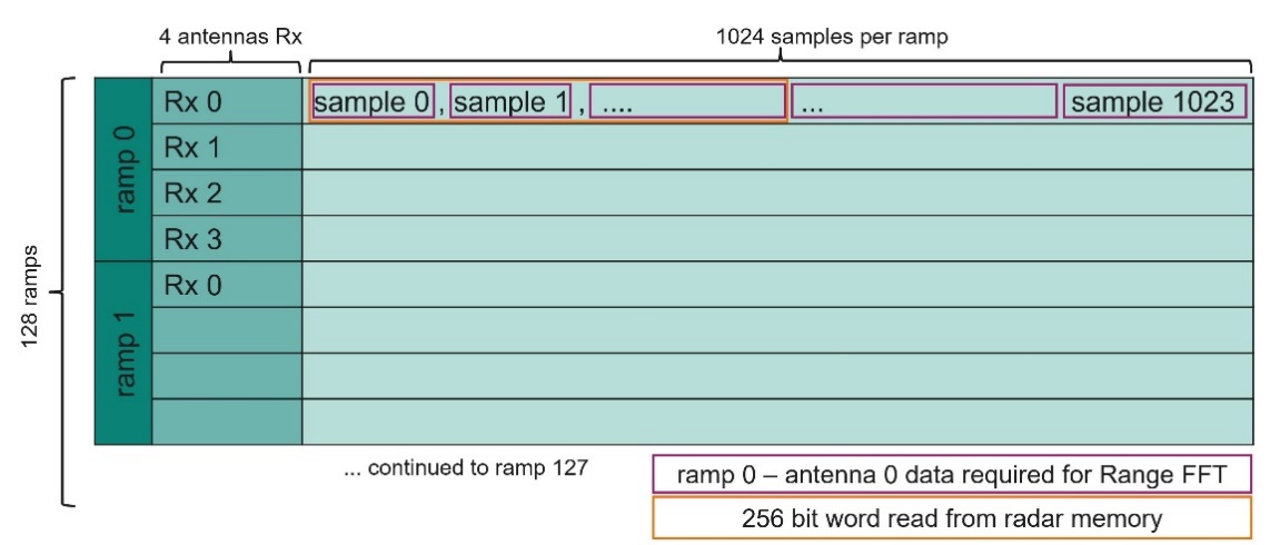
Note: All data fetched in a 256 bit read is used in the same range FFT dataset.
To perform an integration across the results from multiple antenna in the Math2 unit of SPU, data from all antennae has to be available in Math2 for integration. This can be ensured by configuring the input DMA accordingly. By setting the Processing Mode to Integration the input DMA takes care that data from all antennae is available for subsequent integration.
Description | Field | Value | Comment |
|---|---|---|---|
Addressing Mode | TRNSPS | 0 (linear) | Mandatory setting |
Processing Mode | PM | 0,1 (default, integration) | Can be selected |
Number of simultaneous data blocks from RAM (bandwidth optimization) | BLOCKS | 0 (1 data block) | Mandatory setting |
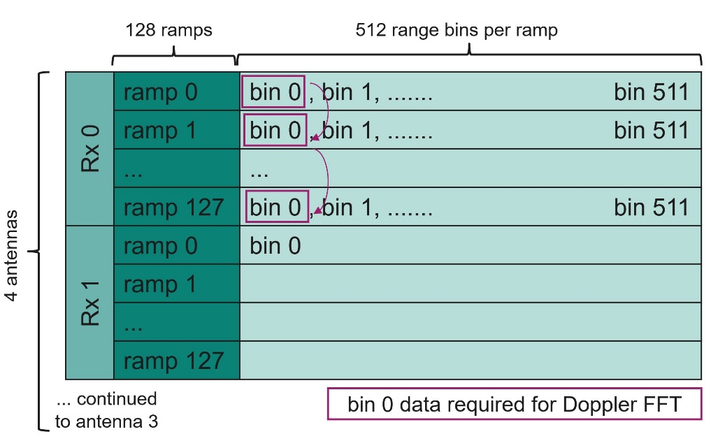
Example data read for second stage (Doppler) FFT: How to use transpose read
This section provides an example where the outer loop offset is set to sample size. Note that examples in Sections
Example data read for first stage (range) FFT
,
Example data read for second stage (Doppler) FFT: How to use transpose read
, and
Setting inner loop offset to sample size
differ with respect to which loop is being set to sample size. The mandatory settings for addressing mode, processing mode and number of blocks described in each section also apply in cases of different concrete settings of e.g., number of ramps and in cases where the other two loops are switched.
In many cases in radar processing the first (range) FFT is followed by a second FFT referred to as Doppler FFT. This FFT is performed accross all ramps of a dedicated range bin of a dedicated anteannae. The data that the input DMA needs to read for this Doppler FFT is marked in purple in
Figure 4
. As consecutive samples to be used as inputs to the FFT are stored in non-consecutive addresses in Radar Memory, address transposition is required. This is supported by the input DMA with a hardware transpose unit and is enabled via selection of transpose addressing mode. As the outer loop offset is set to sample size, integration mode needs to be enabled as well (compare mandatory setting in
Table 5
).
Figure 4. Radar data structure in Radar Memory after range FFT
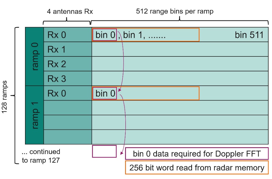
Note: To make efficient use of the entire 256-bit word read bandwidth optimization can be enabled.
Loop parameter setting for the second stage FFT example are provided in
Table 4
. Note that the number of samples is set to the number of range bins in this case.
Name | Abbreviation | Value |
|---|---|---|
Bin loop offset | blo | |
Inner loop offset | ilo | |
Outer loop offset | olo | sample size in bytes |
Bin loop repeat | blr | |
Inner loop repeat | ilr | |
Outer loop repeat | olr |
In the example sketched in
Figure 4
, the orange rectangle indicates the 256-bit word read of the input DMA from Radar Memory. When retaining the current configuration, the full 256-bit word read is not utilized efficiently, resulting in only the first range bin (e.g. bin ‘0’ in the first read) being written to the buffer memory.
To avoid discarding data and wasting bandwidth, build multiple data blocks in buffer memory by setting the BLOCKS bitfield to a value other than ‘0’. This is referred to as bandwith optimization.
Description | Field | Value | Comment |
|---|---|---|---|
Addressing Mode | TRNSPS | 1 (transpose) | Mandatory setting |
Processing Mode | PM | 1 (integration) | Mandatory setting |
Number of simultaneous data blocks from RAM (bandwidth optimization) | BLOCKS | 0,1,3,7 (1,2,4,8 data blocks) | Can be selected |
Setting the BLOCKS parameter to ‘0’ results in one dataset being stored in buffer memory at a time. The first buffer is sketched in
Figure 5
.
Figure 5. Data structure in first buffer of input DMA with bandwidth optimization disabled (BLOCKS = 0)
Setting the BLOCKS parameter to ‘3’ results in four datasets being stored in buffer at a time. The first buffer is sketched in
Figure 6
.
Note: The bin offset and bin repeat values do not need to be adapted when changing the BLOCKS parameter.
Figure 6. Data structure in first buffer of input DMA with bandwidth optimization enabled (BLOCKS = 3)
Setting inner loop offset to sample size
This section provides an example where the inner loop offset is set to sample size. Note that examples in Sections
Example data read for first stage (range) FFT
,
Example data read for second stage (Doppler) FFT: How to use transpose read
, and
Setting inner loop offset to sample size
differ with respect to which loop is being set to sample size. The mandatory settings for addressing mode, processing mode and number of blocks described in each section also apply in cases of different concrete settings of e.g., number of ramps and in cases where the other two loops are switched.
The second case in which consecutive samples to be used as inputs to the FFT are stored in non-consecutive addresses in Radar Memory is sketched in
Figure 7
.
Figure 7. Radar data is structured in Radar Memory after range FFT
Transpose addressing needs to be selected.
Note: In this case the inner loop offset is set to sample size and integration mode is not supported in this case ( Table 6 ). Additionally, bandwidth optimization is not possible and the number of blocks must be set to ‘1’ (number of blocks is equal to BLOCKS field value ‘+1’).
Name | Abbreviation | Value |
|---|---|---|
Bin loop offset | blo | |
Inner loop offset | ilo | sample size in bytes |
Outer loop offset | olo | |
Bin loop repeat | blr | |
Inner loop repeat | ilr | |
Outer loop repeat | olr |
Description | Field | Value | Comment |
|---|---|---|---|
Addressing Mode | TRNSPS | 1 (transpose) | Mandatory setting |
Processing Mode | PM | 0 (default) | integration mode not supported |
Number of simultaneous data blocks from RAM (bandwidth optimization) | BLOCKS | 0 (1 data block) | Mandatory setting |
Additional limitations to consider
The buffer RAM size limit of 32 KBytes
Input and output DMA have a buffer RAM size limit of 32 KBytes that has to be considered. Applying a transpose read with a high number of ramps and bandwidth optimization enabled might cause violation of the buffer limits:
Example 1: Buffer limit not violated: 256 ramps * 6 antennas * 4 Data blocks * 4 Byte per sample= 24.5 KByte
Example 2: Buffer limit violated: 256 ramps * 6 antennas * 8 Data blocks * 4 Byte per sample = 49 KByte
32-byte data alignment in Radar Memory
Each dataset in memory starts at a 32-byte aligned address. This allows the bandwidth optimization hardware to function and is enforced by the output Data Manager. This restriction has to be observed when using software to build data arrays in memory for reading by the input Data Manager.
Maximum number of 2028 bins in an FFT dataset
The maximum number of bins supported in an FFT dataset is 2048.
Note: Setting a Bin Loop Repeat value for an FFT size greater than ID_RM_BLR.BLR > 2047 is not supported and should be avoided.
Using RIF input
The input DMA operates either with the RIF or the Radar Memory (EMEM) as data source (compare
Figure 1
). This section describes the use of RIF data as input.
The RIF provides a parallel memory interface to the SPU unit with a 32-bit bus width. When loading data from the RIF or RIFs, processing mode is always default and the input data format and number of antennae must be aligned with the RIF configuration settings.
The SPU expects 16 bit signed Qm.n integers as an input from the RIF, which is delivered to the SPU in a 32-bit packet. While the RIF accepts a wider range of formats it is responsible for adjusting the direction, data length (16 bits) and format of the incoming ADC data so it fits the SPU RIF input format.
Configuration setting for using the RIF as a data source for input DMA are:
Data source (ADC IF 0 or ADC IF 1 or both)
Ramps per measurement cycle
Number of active antennae
Input format (signed or unsigned, real, or complex)
Samples per ramp
The input DMA implements a ramp counter (referred to as partial acquisition counter PACTR) which can be used to detect if excess data is received or to allow for a delay of start of processing of the SPU. The counter can be configured to generate an error or an interrupt if a particular value is reached.
Working principles of output DMA
The output DMA Engine has eight independent data channels with one output FIFO per result source (e.g., FFT, NCI, LOG2). The data width of the output DMA write path to the Radar Memory is 256-bit.
For each output channel, a base address can be configured. The write address will be incremented automatically so that the results of each channel are stored as an array in memory starting from the defined base address. Each FFT result always starts at a 256 bit (32 byte) aligned address. This is mandatory if the data is to be read back into the SPU as the read operations controlled by the input Data Manager require the start address of each dataset to be 256-bit aligned.
The exception is the “In Place FFT” mode for writing the FFT results to the same memory location as the input data used for the FFT. In this case, the start address is configurable while the address sequence is calculated using the input DMA Engine Loop Repeat and Loop Offset parameters. Input DMA Engine Loop Repeat and Loop Offset parameters are inherited from the input DMA setting. In this case the input and output data size in Bytes must be the same.
References
Infineon Technologies AG:
AURIX™ TC3xx User Manual Part-1
;
Available online
Revision history
Document revision | Date | Description of changes |
|---|---|---|
1.0 | 2024-08-05 | Initial release |
1.1 | 2025-05-28 | Template update; no content update |