AP32385 Enhanced Delta-Sigma ADC (EDSADC) basics
2nd Generation (TC3xx) 32-bit TriCore™ AURIX™ microcontrollers
About this document
Scope and purpose
The Infineon TC3xx microcontroller family provides EDSADC (Enhanced Delta-Sigma ADC) as well as EVADC (Enhanced Versatile ADC).
The delta-sigma technology is one of the most widely used analog to digital conversion methods. It samples the analog input signal at a very high frequency, which is normally hundreds of times faster than the digital result output rate. Each digital output is the average value of several samples. In this document we introduce the basic features of EDSADC and its typical configuration in automotive applications.
This document describes the EDSADC electric parameters, components, digital connection with other peripherals, calibration methods, and result handling.
Intended audience
This document is intended for hardware and software engineers who are designing EDSADC applications.
EDSADC features
The TC3xx family of products has different numbers of EDSADC modules (up to 14x).
Unlike EVADC, each EDSADC module is equipped with 1 pair of differential input channels (single ended connection is also possible). Some EDSADC modules, but not all, have a multiplexer to allow switching between different pins.
As with other peripherals, the EDSADC module is connected to the cores via the SPB bus. EDSADC in general is able to generate a higher Effective Number of Bits (ENoB).
The main EDSADC features are:
-
Switched-capacitance input structure
- Input voltage range 0…5 V
- Common mode voltage: VAREF / x (x = 2, 4, 8), connection selectable for each pin (input pin, VAREF, VAGND or VREFX)
- Programmable gain (1:1 / 1:2 / 1:4)
- DC offset <5 mVDC, gain error < ±0.2% (calibrated, on product level)
- Equivalent input impedance 500 kΩ typ. (for gain = 1, fMOD = 26.67 MHz)
-
On-chip modulator, single-bit second-order feed-forward modulator, sample frequency 16 … 40 MHz
-
Options to connect external standard DS modulators
- Selectable data stream inputs
- Selectable DS clock input or output
-
Demodulator (concatenated hardware filter stages)
- Configurable CIC filter with decimation rates of 4…1024 (with pre-CIC enabled)
- Overshoot compensation filter, optional
- FIR filter with 8 coefficients (10-bit) with decimation rate 2 (FIR0)
- FIR filter with 28 coefficients (10-bit) with decimation rate 1 or 2 (FIR1)
Pass Band:
| Passband | condition |
|---|---|
fd/3 | FIR1 decimation rate = 2:1 |
fd/6 | FIR1 decimation rate = 1:1 |
Pass band ripple dfPB < ±1% | |
Stop band attenuation:
| Bandwidth | Attenuation |
|---|---|
0.5…1 × fd | > 40 dB |
1…1.5 × fd | > 45 dB |
1.5…2 × fd | > 50 dB |
2…2.5 × fd | > 55 dB |
2.5…OSR/2 × fd | > 60 dB |
-
Optional high-pass filter for DC compensation (f-3dB = 10-5 × fd), configurable
-
Hardware offset/gain calibration and compensation
-
Support for resolver applications
- Carrier signal generator (differential sine output). An additional external analog circuit is needed to transform the digital output from carrier signal generator into a sine wave for example.
- Signal evaluation including rectification, delay compensation and carrier elimination.
-
Automatic limit checking
- Two-level boundary comparator.
- Separate indication signals (hardware signal to notify comparison result: above the upper limit, within the defined band or below the lower limit).
In case TJ ≤ 150°C and fPB = 30 kHz, the SNR (Signal to Noise Ratio) is at least 80 dB, corresponding to an ENoB of approximately 13 bits.
Modulator and filter chain
The modulator and demodulator (also called the filter chain) are the kernel parts of the EDSADC. The on-chip filter stages generate digital results from the selected modulator signal.
Figure 1. EDSADC block diagram
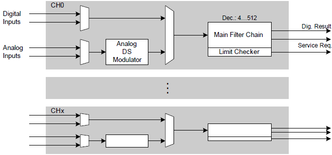
If necessary an external modulator can also be selected and the digital input will directly connect to the main filter chain. A typical use case for an external modulator can be for the purpose of galvanic de-coupling.
Figure 2. Main filter chain (demodulator)
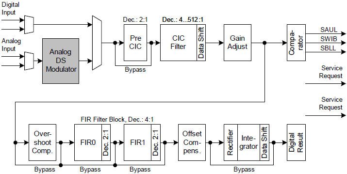
Filter chain
The filter chain configuration determines the attenuation and group delay properties of the filter. The configurable CIC (Cascaded Integrator Comb) filter, also known as a SINC filter, provides the basic filtering and decimation with a selectable decimation rate.
There are 2 FIR filters:
-
FIR0 with a fixed decimation rate of 2
-
FIR1 with a configurable decimation rate (1 or 2)
The filters allow effective signal shaping by attenuating the upper frequencies of the signal spectrum. The digital signal will go through the main CIC filter and 2 consecutive FIR filters.
The high-pass filter provides offset compensation by removing the DC component of the input signal. The Pre-CIC is provided mainly for backwards compatibility (on TC2xx, the decimation rate of FIR1 is fixed to 2, and this Pre-CIC can be optionally enabled to have the same total decimation rate).
The on-chip carrier signal generator produces a PWM signal that induces a sine signal in the excitation coil of the resolver.
Synchronization of each input signal to the carrier signal ensures correct integration of the resolver input signals. The integrator integrates the result values generated during the defined integration window by adding a configurable number of values to build the final result value. Integration can be used to measure currents through shunt resistors at defined positions in the signal waveform. It can also remove the carrier signal component in the resolver application.
| Bandwidth (kHz) | Min SNR (dB) | ENoB | Condition |
|---|---|---|---|
100 | 74 | 12 | TJ ≤ 150°C |
50 | 78 | 12.7 | TJ ≤ 150°C |
30 | 80 | 13 | TJ ≤ 150°C |
In case EDSADC is in single ended mode, around 6 dB (corresponds to 1 ENoB) will be lost for each case.
The following table shows the SNR as well as the input current under more cases with Gain =
- For other gains, the input leakage is proportional to the gain factor (linear). fPER on TC3xx is fixed to 160 MHz.
Modulator frequency fMOD | Input current IRMS1 | fPB < 10 kHz2 | fPB < 30 kHz | fPB < 50 kHz3 | fPB < 100 kHz3 | ||||
|---|---|---|---|---|---|---|---|---|---|
SNR | OSR | SNR4 | OSR | SNR4 | OSR | SNR4 | OSR | ||
16 MHz (fPER/10) | 6 µA | ≥ 78 dB | ≥ 267 | ≥78 dB | ≥ 178 | ≥74 dB | ≥ 107 | ≥65 dB | ≥ 54 |
20 MHz (fPER/8) | 7.5 µA | ≥ 80 dB | ≥ 334 | ≥78 dB | ≥ 223 | ≥74 dB | ≥ 134 | ≥68 dB5 | ≥ 67 |
26.67 MHz (fPER/6)6 | 10 µA | ≥ 80 dB | ≥ 445 | ≥80 dB | ≥ 297 | ≥78 dB | ≥ 178 | ≥74 dB | ≥ 89 |
40 MHz (fPER/4) | 15 µA | ≥ 80 dB | ≥ 667 | ≥80 dB | ≥ 445 | ≥78 dB | ≥ 267 | ≥74 dB | ≥ 134 |
These typical values refer to an input voltage of 5 V and the typical value of the switched capacitor:
IRMS = 5 V × fMOD × 2 × CSW. The equivalent input impedance can be calculated by 5V / IRMS.
Hardware triggers
EDSADC generates a continuous output stream once the modulator is enabled.
Hardware triggers are used for the following features:
Integration trigger
The external signal defines the integration window; i.e. the timespan during which result values are integrated. A typical usage for the integrator is to cancel the carrier signal in resolver application.
Timestamp trigger
The external signal requests the actualization of the timestamp register. This feature is necessary for software interpolation, because the EDSADC outputs a digital result at a fixed rate of fd.
Input multiplexer trigger
The external signal requests the switching of the analog input multiplexer to the next lower input, or to the defined start value, respectively.
Modulator run gate
The on-chip modulator can be controlled by an external gate signal while it is enabled. In this case it can be disabled temporarily to save power. Please note that the modulator needs some wakeup time when the gate signal changes from inactive to active. The wakeup time is documented in the user manual.
Service request gate
Service requests for the filter chain can be restricted to the high or low times of the selected trigger signal.
Calibration and Result interpretation
Offset calibration and gain calibration are done by hardware. The calibration values are determined automatically by a hardware algorithm. This can be triggered initially after a reset or repeatedly during operation, for example when TJ changes more than 20°C.
The time needed for calibration depends on modulator frequency, decimation rate and gain. Please see the user manual for the calibration duration.
The digital result of EDSADC is stored in 2’s complement format with 16 digits (1 sign bit and 15 value bits).
The digital result in stored in result register RESMx.RESULT.
The result is normalized to ±25000 after reset:
-
-25000 represents -5V
-
25000 represents 5V
-
values in between are linear
If full scale is expected, to for example minimize quantization errors, it is possible to use the full range from -32767 to 32766. This is achieved by configuring GAINCORR.
As the digital result register is 32-bit wide, it is possible to put 2 results to the higher and lower halves of the result register respectively and read them out together (this is also convenient for interpolation calculations).
The digital result output rate (fd) is relatively high and therefore a hardware FIFO feature is provided to allow for a flexible read out. The maximum FIFO depth is 4.
Result FIFO
EDSADC results can be placed in FIFO and later read out (enabled by bit field DRM). Together with time-stamp feature (enabled by bit TSM), the following modes are supported:
| Read mode | FIFO disabled This mode is similar to TC2xx, which has no FIFO. | ||||
|---|---|---|---|---|---|
Content in result register EDSADC_RESMx | |||||
TSM = 0 DRM = 1 | No FIFO | [31...16] bits | 0 | [15...0] bits | Result |
TSM = 1 DRM = 1 | No FIFO | [31...16] bits | Timstamp | [15...0] bits | Result |
DRM = 0 or 2 means the FIFO is enabled (DRM = 3 is reserved and shall not be used). Please note the FIFO structure is transparent to the user and the user must read the EDSADC_RESMx result register several times to fetch contents stored in FIFO. The FIFO filled level is indicated by the bit field EDSADC_RFCx.FILL.
FIFO overflow and underflow errors are indicated by the bit fields EDSADC_RFC.WRERR and RDERR respectively.
| Read mode | FIFO enabled DRM = 0 | ||||
|---|---|---|---|---|---|
Content in result register EDSADC_RESMx | |||||
TSM = 0 DRM = 0 | 4th read | [31...16] bits | Sign extention | [15...0] bits | Result 3 |
3rd read | [31...16] bits | Sign extention | [15...0] bits | Result 2 | |
2nd read | [31...16] bits | Sign extention | [15...0] bits | Result 1 | |
1st read | [31...16] bits | Sign extention | [15...0] bits | Result 0 | |
TSM = 1 DRM = 0 | 4th read | [31...16] bits | Sign extention | [15...0] bits | 2nd result after timestamp |
3rd read | [31...16] bits | Sign extention | [15...0] bits | 1st result after timestamp | |
2nd read | [31...16] bits | Sign extention | [15...0] bits | Result before or at timestamp | |
1st read | [31...16] bits | Shall be ignored by user | [15...0] bits | Timstamp | |
| Read mode | FIFO enabled DRM = 2 | ||||
|---|---|---|---|---|---|
Content in result register EDSADC_RESMx | |||||
TSM = 0 DRM = 2 | 4th read | [31...16] bits | Result 7 | [15...0] bits | Result 6 |
3rd read | [31...16] bits | Result 5 | [15...0] bits | Result 4 | |
2nd read | [31...16] bits | Result 3 | [15...0] bits | Result 2 | |
1st read | [31...16] bits | Result 1 | [15...0] bits | Result 0 | |
TSM = 1 DRM = 2 | 4th read | [31...16] bits | 6th result after timestamp | [15...0] bits | 5th result after timestamp |
3rd read | [31...16] bits | 4th result after timestamp | [15...0] bits | 3rd result after timestamp | |
2nd read | [31...16] bits | 2nd result after timestamp | [15...0] bits | 1st result after timestamp | |
1st read | [31...16] bits | Result before or at timestamp | [15...0] bits | Timstamp | |
Revision History
Document revision | Date | Description of change |
|---|---|---|
All | First version. | |
V1.1 | Added chapter Result FIFO. Updated Table 4 according to User Manual V2.0. | |
V1.2 | 2024-04-17 | Template update; no content update. |
These typical values refer to an input voltage of 5 V and the typical value of the switched capacitor:
IRMS = 5 V × fMOD × 2 × CSW. The equivalent input impedance can be calculated by 5V / IRMS.