AP32368 PCB design guidelines for Gbit-Ethernet interface
32-bit TriCore™ AURIX™ TC3xx microcontroller
About this document
Scope and purpose
The TC33x, TC35x, TC36x, TC37x, TC38x, and TC39xED are part of the AURIX™ TC3xx family of 32-bit microcontroller products. They are available in different packages and might require a PCB carefully designed for electromagnetic compatibility.
This document provides product-specific PCB design recommendations and guidelines for the Ethernet Interface (MAC – PHY) of the AURIX™ TC3xx, and should be read in conjunction with the Infineon PCB Design Guidelines for Microcontrollers (AP24026), AP32334 and AP32335, which give general design rule information for PCB design.
Intended audience
This document is intended for anyone who designs with the AURIX™ TC3xx microcontroller and needs design recommendations regarding to the EMC optimized PCB design.
Supply domains
The microcontroller has the following supply domains which should be individually de-coupled:
- VDD = 1.25 V for Core
- VDDP3 = 3.3 V for Flash supply
- VFLEX, VFLEX2 = 3.3 V for Ethernet Port supply
- VEXT = 5 V for default GPIO supply
- VDDM = 3.3 V, or 5 V for ADC
The power supply feeding from the regulator outputs to each domain can be made on a supply layer (POWER).
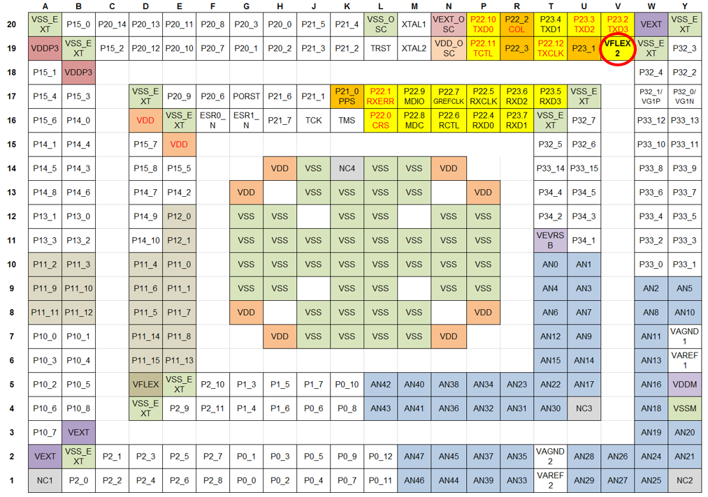
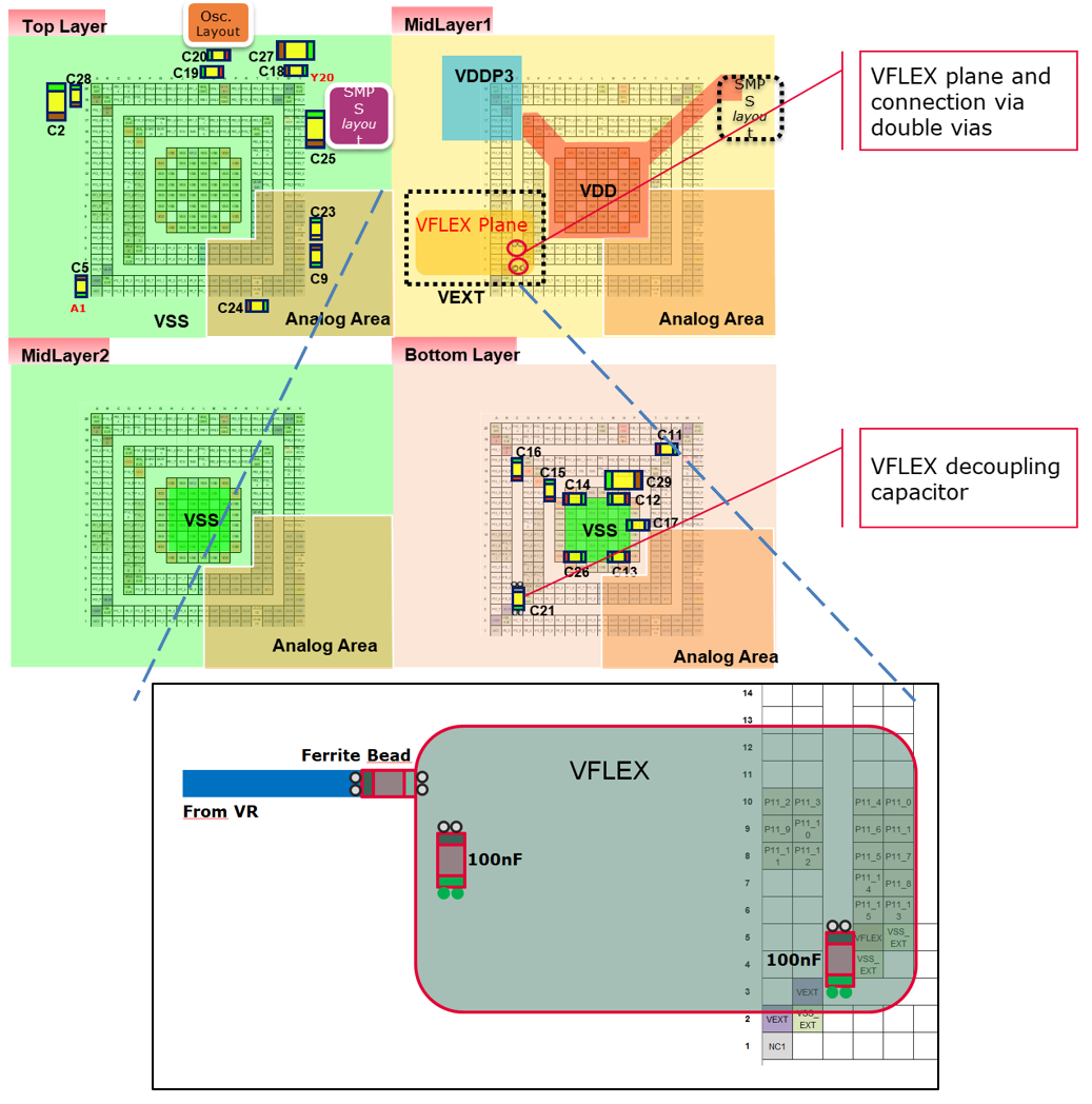
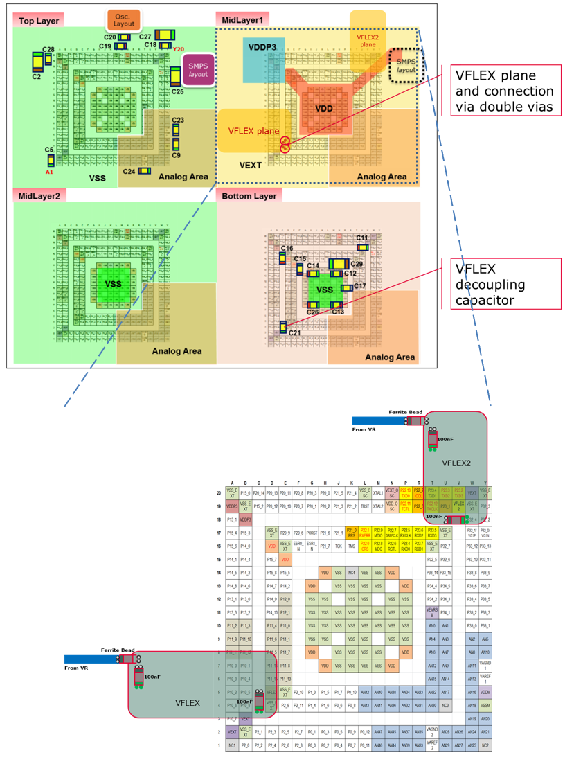
The supply pin of the Gbit-Ethernet Module is pin VFLEX (D5 or J10).
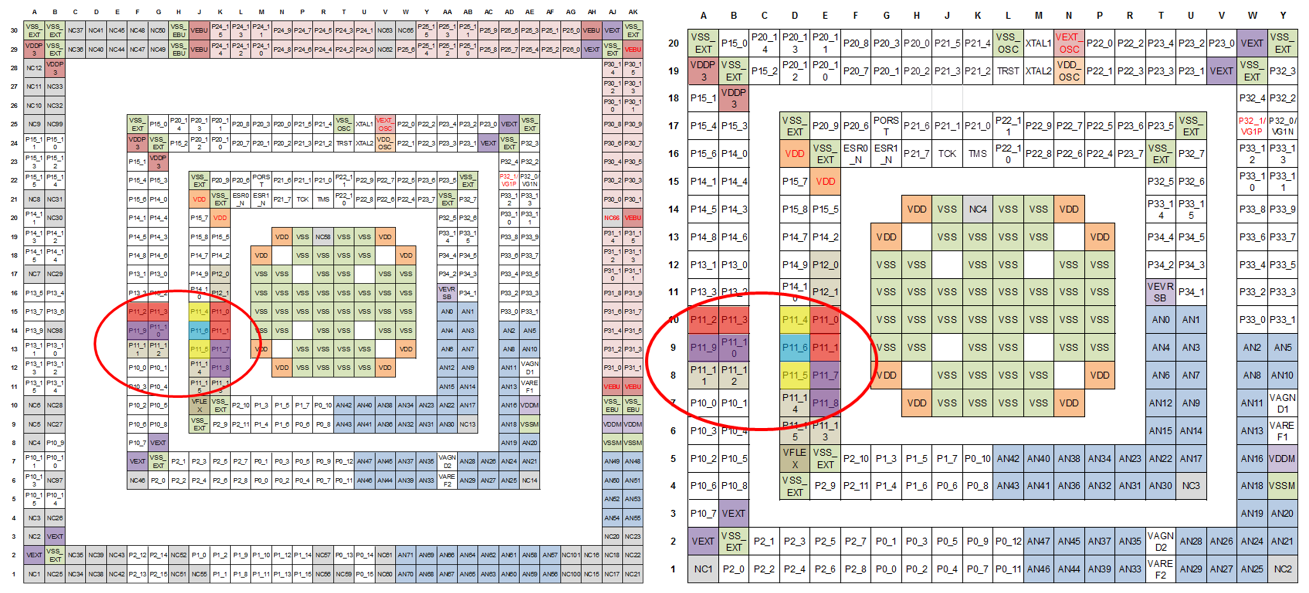
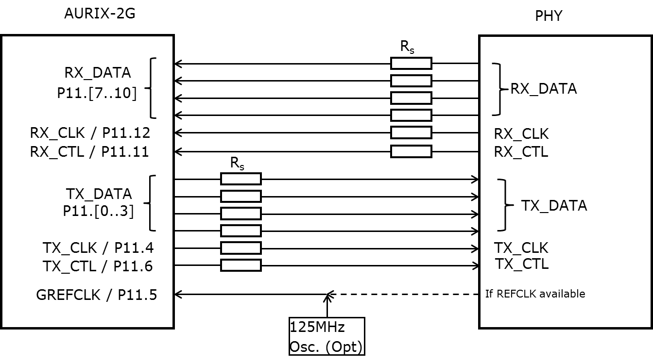
Pinouts with one Gbit Ethernet interface
Pinout with two Gbit Ethernet interfaces
PCB design
This chapter introduces some ground rules for EMC-friendly PCB layout for the Gbit-Ethernet interface.
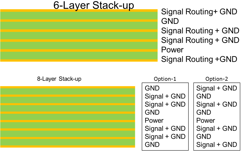
Selection of stack-up
Selection of the correct stack-up for a high-speed board should be made at the beginning of the board design because the selection can have an effect on the routing and impedance control of the traces. Impedance control of the traces is one of the main parameters of the high-speed design.
The following issues must be considered:
- It should be guaranteed that high-speed lines have a solid GND reference without interruption of the impedance continuity.
- Signal lines must have minimum distance to reference the plane layer also in conjunction with controlled impedance.
- Ensure, as much as possible, a plane capacitance for the supply domains.
- Avoid vias or layer change on high-speed signals.
Since the discrete board de-coupling capacitors can only be effective up to 200 MHz, the plane de-coupling should be used where possible.
The stack-up should be selected so that you can build a power plane capacitance and have the benefit of the high frequency de-coupling effect which could be effective above 200 MHz. Figure 3 shows sample stack-up for six, and eight layer PCB.
Impedance controlled design of traces
Design of traces for high-speed signals is critical. They should be designed to have a trace impedance of typically 50-60 Ohm.
There are two types of transmission lines for trace implementation:
- Microstrip
- Stripline
It is recommended to design GBit-Ethernet interface lines as stripline with controlled impedance of 50-60 Ohm. In special cases these impedance values can excide that recommendation. In this case simulations shell be done.
Striplines

The following points are design references:
It is recommended to have a distance of two times the trace width between single-ended traces.
- Transmit and receive lines group should also be separated with a distance of >2 mm if possible.
- Do not route signal lines parallel to Tx/Rx signals on the adjacent layers to avoid coupling.
- Place possible noise sources or sensitive signals away from the high-speed signals.
- Keep the trace length of all Ethernet interface signals equal and as short as possible.
- It is recommended to keep the trace lengths within the Tx and Rx trace bundles at matching lengths and as short as possible (~250 – 400 um).
- The Tx_CLK transmit clock trace/stripline shall have a distance of at least >300 um from the neighboring signal traces. The data traces / striplines may have a distance of 125 um between each other.
- It is recommended to use a total trace length less of than 7.5 cm for this interface on the boards. If longer traces are required, always check with simulations.
Always keep the return path of the high-frequency current (lowest inductance path) small.
- Route the signals with adjacent ground reference and avoid signal and reference layer changes.
- Routing ground on each side can help to reduce coupling to other signals.
- Avoid cutting the GND plane by via groups. A solid and uninterrupted GND plane under critical signals must be designed.
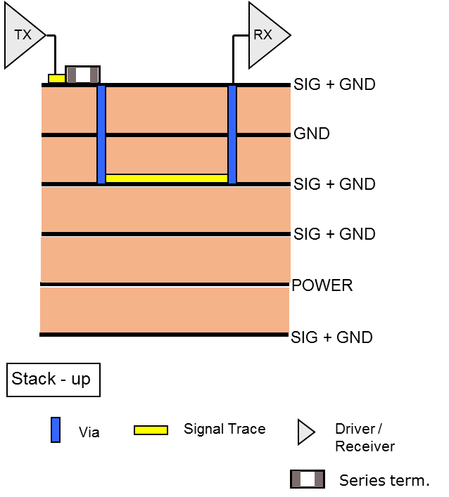
- Route the clock line first and use a straight line for connection.
- Minimize the via count on signal lines (if possible, do not use any).
Termination of transmission lines
There are different types of termination techniques. It is recommended to use series termination (or source termination). The recommended start value is ~39 Ω. This value shell be confirmed by simulation of the customer PCB from the customer.
This is normally used by the single ended lines where the output driver has lower impedance than the transmission line. In this case the series termination is added to the output of the driver to match the line impedance.
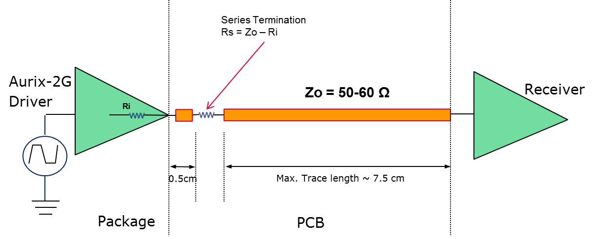
- Place the resistor very close to the source driver.
- Do not use daisy-chain topology.
IBIS Simulation example
A high-speed simulation using IBIS files is a kind of standard during designs of PCBs. Infineon Technologies provides for each device of the TC3xx these kinds of files. The surrounding temperature is an aspect which shell be checked as well.
Out of the chapter before the following model was used for that example.
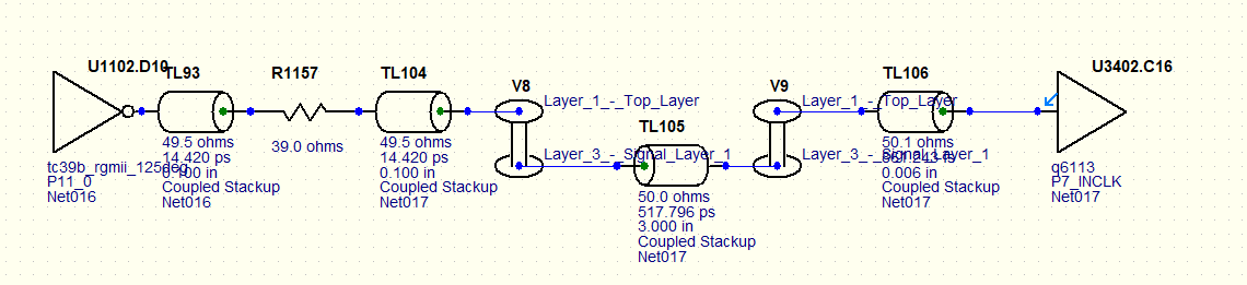
The simulated example results in the following waveform for a typical use case.
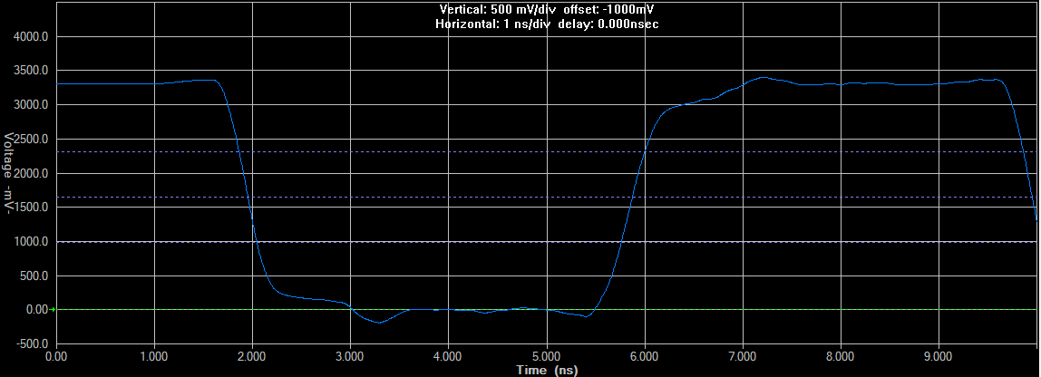
While looking to the slow and fast corner of that simulation, adaptions of the series termination or transmission line impedance value is required to meet timings and over/under shoot values of the connected device.
Board level filtering and de-coupling
De-coupling the Power Distribution Network of the microcontroller IC is critical to the PCB design process because careful selection of the de-coupling capacitors and placement has a big influence on the high-speed performance of the board, and can reduce the emissions. The on-board de-coupling capacitors have an effective range of 1 MHz – 200 MHz. The range above 200 MHz can be covered by using power plane capacitance.
The effectiveness of the de-coupling capacitors depends on the optimum placement and connection type.
- Place capacitors as close as possible to the microcontroller.
- Keep the interconnection inductance of capacitors to the microcontroller as low as possible.
Use low effective series resistance and inductance (ESR and ESL) capacitors.
- Since parasitic inductance is the limiting factor of the capacitor response to high frequency demand of current from the device, the ESL of the capacitor and the connection inductance should be selected so that the optimum value for the design is reached.
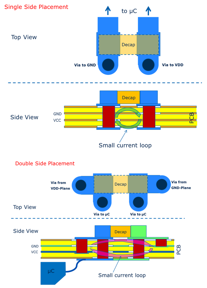
Connect capacitors with vias close to the side of the pads as shown in Figure 10.
- Use side placement of the vias to reduce the current loop.
- If a solid power plane can be built (without cutting the plane and impedance discontinuity), the de-coupling capacitors can be connected directly to the plane and microcontroller for the case of double side placement.
- Dual vias can be used to reduce the parasitic inductance.
- Solder lands, traces and vias should be optimized for capacitor placement.
Do not use long traces to connect capacitors to GND or to VDD.
- Always keep the return path of the high frequency current (lowest inductance path) small.
- Select the smallest package available for the capacitors.
- Select capacitors of type: ceramic multilayer X7R or X5R.
- Design a VFLEX / VFLEX2 plane on the power layer to generate a capacitance to filter the high frequency noise at VEXT net which is effective above 200 MHz.
- Use two 100 nF de-coupling capacitor for each VFLEX / VFLEX2 net. One should be connected directly to VFLEX (D5) / VFLEX2 (V19) and the VSS (D4/W19) balls of the BGA package with vias. The other 100nF capacitor should be connected to plane area (see Figure 9 and 10). The second 100nF capacitor reduces the emission ~3 dB µV (towards to VR).
- Use at least 2 vias to connect VFLEX / VFLEX2 nets to VSS (D5/D4 pins/V19/W19) to the de-coupling capacitor on the bottom layer.
- Use a ferrite bead to de-couple the main supply line from the VFLEX (2) net (consider the design parameter like impedance at 100 MHz, rated current and DC-Resistance). The Ferrite Bead reduces the emission towards to VR ~20 dB µV.
Revision history
| Document revision | Date | Description of change |
|---|---|---|
V1.0 | Initial version | |
V1.1 | Figure-2, 6 and 8 updated, Ferrite bead and 2x100nF added to VFLEX net. | |
V1.2 | Figure-5, -9, Impedance value and max. Trace length updated. Chapter 1.2 added. | |
V1.3 | Figure -9 split in to Figure-9 and Figure-10 | |
V1.4 | Add new chapter 2.4, adaption of some text parts in chapter 2.2 and 2.3 | |
V1.5 | 2024-04-17 | Template update; no content update. |