AP32398 HSCT Jitter considerations
TriCore™ AURIX™ 2nd Generation Family
About this document
Scope and purpose
Considerations for the Bit Error Rate (BER) of an HSCT connection.
Intended audience
This document is intended for engineers designing ASICs (Application Specific Integrated Circuits) containing the HSSL/HSCT interface, and for application engineers designing hardware systems based on the HSSL/HSCT interface.
Introduction
At physical layer level, the HSSL/HSCT is a bi-directional Double-Data-Rate (DDR) serial link with a common, shared, relatively low frequency clock signal, called SysClk. The device driving the SysClk is called master, and the device receiving the SysClk is called slave (see Figure 1).
Both the master and the slave contain dedicated PLLs generating the high frequency clock signals necessary for the high speed baud rates at the data lines. A typical frequency for the SysClk is 20MHz, and the standard high speed data-rate is 320Mbit/s DDR, corresponding to a data signal with frequency of 160MHz.
To ensure proper data transmission, the slave device must use the SysClk as reference clock for its PLL. This SysClk is derived directly from the XTAL oscillator, which serves as a reference for the master device.
The slave device, which does not have its own additional crystal oscillator, uses the SysClk for generating the clock not only for the HSSL link, but for the whole system; therefore the name “SysClk”.
Figure 1. HSSL/HSCT Connection

Bit Error Rate
The main topic of this document is the Bit Error Rate (BER) of an HSCT connection. The focus lies on BER20, which is the Bit Error Rate when the system is working with a SysClk frequency of 20MHz.
The BER depends strongly on the jitter of the SysClk signal. The dependencies are as follows:
The jitter on the SysClk signal has direct impact on the output jitter of the slave PLL (within the PLL bandwidth).
In the master device, the master PLL determines the jitter of the sampling points, and the slave PLL determines the jitter of the received data signal.
In the slave device, the slave PLL determines the jitter of the sampling points, and the master PLL determines the jitter of the received data signal.
As a consequence, the jitter of the SysClk signal directly affects the jitter of the received data at the master device, and the jitter of the sampling points at the slave device.
The Total Jitter (TJ) of a signal consists of:
- Deterministic Jitter (DJ), which is bounded
- The DJ always remains within certain hard limits, independent of the observation time.
- Random Jitter (RJ), which is not bounded
- The RJ is represented by a Gaussian distribution.
- TJ = RJPP + DJ
The rms (root mean square) parameter of the RJ corresponds to one σ of such distribution. It is not bounded; therefore, if the observation time is long enough, any clock edge deviation can occur. It is only a question of probability and time. For this reason, the peak-to-peak value of RJ is not precisely measurable in practice, and a more appropriate way to define it is by calculation based on the one σ value and on the level of confidence needed for a specific application, so that there is a given probability that the specific occurrence of the time deviation does not exceed the calculated RJPP.
For serial transmission, the peak-to-peak Random Jitter is defined:
RJPP = 2×Q×σ (or ±Q�×σ)
where Q is the factor that depends on the target Bit Error Rate (BER)
For BER20 = 10-12, Q=7
Data Eye and Jitter
The HSCT PLL in the AURIX™ microcontroller family is a five phase PLL. During the synchronization sequence, there is a mechanism selecting the optimal phase. The selected phase is used during the following frame to sample all the bits. The following diagram shows the data eye and the sampling phases:
Figure 2. Data Eye

For a serial interface, where both data signals and sampling clock signals are affected by jitter, TJ is defined as the sum of Deterministic Jitter (DJ) and Random Jitter (RJ) as:
where:
- DJTX → DJ of the transmitted signal (data)
- DJRX → DJ of the sampling clock at the receiver (sampling phase)
- Q → multiplication factor according to the Bit Error Rate (BER) which has to be achieved
- σTX → RMS Random Jitter affecting the data signal
- σRX → RMS Random Jitter affecting the sampling signal
Q is defined as:
BER = 10-12 → Q=7
BER = 10-9 → Q=6
As the Random Jitter of the transmitter and the receiver are not correlated with each other, the standard deviation of the resulting RJ is the square root of the sum of squares of the standard deviations of the single components, as indicated in the formula above.
σTX can be directly measured as the RJ out of the eye diagram (through jitter de-composition in deterministic and random contributions) or indirectly by integrating the phase noise plot.
Measurements show that with fSYSCLK = 20 MHz, in worst case:
σTX = 80ps
σRX is measured as the jitter accumulated over the whole frame length (288bit), because the sampling phase is fixed for the whole frame once the sync pattern has been recognized.
To specify σRX the RMS value of the accumulated jitter at the 288th cycle has to be taken into account.

In case of an overshoot of the accumulated jitter (red circle in the picture above) or a high deterministic component (DJ), which will result in a modulation on top of the ideal (random) accumulated jitter curve, the worst cycle has to be taken into account and the σRX has to be measured from this point.
All the data is available during the measurement producing the accumulated jitter curve, and measurements from Tc3XX A-step show no significant overshoot in the curve, so the DJ component can be omitted and the σRX was measured at cycle no. 300.
Measurements show that with fSYSCLK = 20 MHz, in worst case:
σRX = 100ps
As a consequence, assuming Master and Slave side are running under the same conditions, with:
fSYSCLK =20 MHz
DJ=0
BER = 10-12
Then the TJ of the system is:
1793ps < 2500pswhere 2500ps=2*1250ps is the limit to be respected in order to assure a BER = 10-12, as depicted in Figure 2, where the worst case sampling phase has been considered.
The calculations shown have been performed with the absolute worst case values.
Integrated Phase Noise and Random Jitter
The critical parameter standard deviation of the RJ can be determined by measuring the phase noise of a signal and integrating the phase noise curve.
For the ARUIX™ family of microcontrollers, the phase noise characteristic of the SysClk signal has been measured and the Integrated Phase Noise (IPN) parameter has been determined.
The value reached with the maximum power pattern running on the master microcontroller is:
- IPN=-49dBc, corresponding to JABS20 = σTX = 40ps*
The value reached with no application running on the master microcontroller is:
- IPN=-67dBc, corresponding to JABS20 = σTX = 5ps*
* Integration range from 10kHz to 10MHz, SysClk frequency=20MHz.
Phase Noise Behavior of a PLL
The following section provides some practical considerations regarding the design of an appropriate PLL for a HSSL/HSCT communication channel.
Theoretical considerations
- A PLL acts as a low pass filter for the noise of the reference clock with a corner frequency defined by the PLL bandwidth.
- To keep the contribution of the reference clock noise to the PLL output noise as low as possible, a low PLL bandwidth should be selected.
- A PLL acts as a high pass filter for the noise of the PLL oscillator (DCO Digital Controlled Oscillator or, VCO Voltage Controlled Oscillator) with the corner frequency also defined by the PLL bandwidth.
- To keep the contribution of the DCO noise to the PLL output noise as low as possible, a high PLL bandwidth should be selected.
- The noise of the reference clock (fSYSCLK) is converted into noise of the PLL clock with the factor of 20*log(fPLL/fSYSCLK) within the bandwidth of the PLL.
Practical Considerations
The characteristics of the AURIX™ HSCT PLL are:
- Bandwidth ∾ 1 MHz
- JABS20 ∾ 20-30s
Recommendations and Guidelines for PLL design
In order to keep the influence of the high fSYSCLK jitter as low as possible, it is recommended that:
- PLL bandwidth should be as low as possible (penalty on area is possible)
- DCO free running phase noise should be as good as possible (penalty in current and area are possible)
If these points are considered, the main contributing factor to the PLL phase noise (and jitter) is the noise of the DCO itself.
For low bandwidth a very low phase noise of the oscillator should be the target (with a potential impact on area and current consumption).
Phase noise masks and Transfer Functions
The diagram below shows the phase noise characteristics at the input and at the output of the HSCT PLL in the master and slave device. The phase noise and jitter characteristics have been measured in:
- Maximum power pattern with all modules on the chip active (worst case regarding jitter)
Figure 4. Phase Noise and Transfer Characteristics of the HSCT PLL in AURIX™ Family
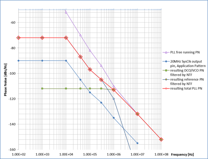
The phase noise plots in the diagram show the behavior and noise transfer functions of the PLL with focus on the reference noise (fSYSCLK) and the PLL free running Phase Noise.
According to the theory, the reference noise is:
- Converted up to the TX frequency (20MHz → 160MHZ)
- Low-pass filtered with the PLLs Noise Transfer Function (NTF) with a bandwidth of ~1MHz.
- The noise of the free-running DCO is high-pass filtered with the bandwidth of ~1MHz.
Combining the filtered noise curves leads to a resulting red curve showing the total phase noise at the output of the locked PLL.
The following PLL parameters:
- DCO frequency = 640MHz
- DCO free running phase noise @1MHz = < -98dBc
Those parameters lead to integrated jitter numbers of:
- JABS20 = 46ps maximum power pattern, all modules with maximum activity
- JABS20 = 6ps test mode, all modules except HSSL/HSCT inactive
PLL fed with fSYSCLK having the phase noise characteristics shown in the diagrams, meets the requirement of JABS20 ≤ 85ps, which is sufficient to fulfill the requirement of BER=10-12.
Revision history
Document version | Date of release | Description of changes |
|---|---|---|
1.0 | 2017-10-12 | Initial version. |
| 1.1 | 2024-02-13 | Template update; no content update. |