AP32402 Integration of TC3xx microcontrollers with TLF35584/TLF35585 power supply
About this document
Scope and purpose
The document describes hardware and software aspects such as system start-up, reset conditions, initialization, configuration of the system supply, safety management with respect to features of system supply, and features of the AURIX™ TC3xx PMS sub-system.
When combined with the system power supply TLF35584/TLF35585, products of the TC3xx microcontroller family provide a very high level of power integration, and together form a complete solution for the power supply sub-system in automotive safety applications.
Both of the TLF power supplies offer integrated microcontroller voltage regulators with an optimized number of system voltage regulators to complement a very broad range of applications. For example, the TLF35584/TLF35585 targets Electric Power Steering and chassis application domain. However, the power supply is not limited to those fields and can therefore be used to fit a wide variety of applications.
Intended audience
This application note is targeted at hardware and software engineers who integrate AURIX™ TC3xx microcontrollers with TLF35584/TLF35585 power supply.
System safety supply hardware integration with AURIX TC3xx products
TLF35584/TLF35585 hardware aspects
Interface and external safety mechanisms
The TLF35584/TLF35585 generates the power for the microcontroller in ‘single supply mode’, which means that a single voltage regulator is used externally as the main power sources, while the rest of voltage rail required for microcontroller start-up is generated by its own means.
In addition to the main voltage regulator, other voltage regulators for the microcontroller supply are also integrated:
- The main voltage regulator QUC.
- The reference voltage regulator for analog features QVR.
- The standby supply for the standby domain and system low power modes QST.
Mandatory: QUC supply generates power to all isolated voltage domains of 5 V or 3.3 V nominal rating. The 5 V or 3.3 V supply defines the VEXT domain voltage and therefore logical levels of the microcontroller IO pads supply. The QUC regulator partially supplies the oscillator/PLL sub-system as it is related to the VEXT domain.
Note:- If the TLF35584/TLF35585 is used in 5 V configuration, an isolated VFLEX domain can be used in 3.3 V configuration with the internally generated 3.3 V voltage.
- It is mandatory to use the QUC regulator as the input supply for the embedded core voltage regulator EVRC. It is not recommended to use an input voltage regulator for EVRC input that is independent from QUC. Therefore, the TC3xx application assumes that the VEXT domain and EVRC input are supplied from the same source.
- A split VEXT and EVRC input supply is allowed while using an external P-N-MOS gate driver with the supply voltage referenced to the EVRC input supply. Such a use case is described in the datasheet for the Infineon TLF11251 P-N-MOS half-bridge with integrated gate driver and an independent split supply.
- The TLF35584/TLF35585 supply provides an optional redundant regulator for the isolated EVRSB power domain VEVRSB. This domain supplies standby features of TC3xx as well as its power management sub-system with safety features such as voltage monitors, redundant back-up clocks, redundant Safety Management Unit (Standby SMU), voltage, and current references for other microcontroller sub-systems. EVRSB input allows a redundant voltage source that is independent from QUC, which is QST standby LDO of TLF35584/TLF35585.
- Mandatory: The ROT-PORST reset interface to the microcontroller generates a warm reset
class to the microcontroller. It is not bi-directional on TLF35584/TLF35585.
Optional: The QVR supply is an integrated LDO for analog domain VDDM/VAREF of the microcontroller. Being independent from the QUC supply, it offers better PSSR (<26 dB) for analog purposes.
PORST is a uni-directional TTL level Power-On Reset input of the microcontroller with an integrated weak pull-down and strong active pull-down for power fail.
The POR output of TLF35584/TLF35585 is an Open-Drain output. An additional external pull-up is required to ensure warm reset de-assertion after all operational conditions are met. It must be dimensioned for proper rise times and current leakage during asserted reset, typically in the range of ~2.2 - 4.7 kOhm. An additional series current limiting resistor is not required. Additional de-glitching of the microcontroller PORST input is implemented with a permanent analog filter of at least 80 ns blocked spike duration and can be additionally adjusted in the microcontroller with a configurable digital filter with a minimum 600 ns blocked duration.
- Optional: The WDI-GPO interface provides a Window Watchdog (WD) service over the
general purpose output of the microcontroller. Typically, a dedicated OS task is
assigned for the periodic service during a strictly defined period of time called an
‘open window’.
Any standard 5 V or 3.3 V pads of the microcontroller can be used for the WDI service. No strict requirement is applied to the microcontroller pad output driver due to the low frequency of the change in this application. TLF35584/TLF35585 uses TTL logical level inputs in the 3.3 V device variant, and a wider logical input range in the 5 V device variant (>3.6 V logic high state).
- Mandatory: The SPI communication channel is used for supply
configuration purposes after start-up and during mode transitions.
Optional: It can be used for servicing a Window WD instead of WDI GPO interface and for Functional (Q/A) Watchdog.
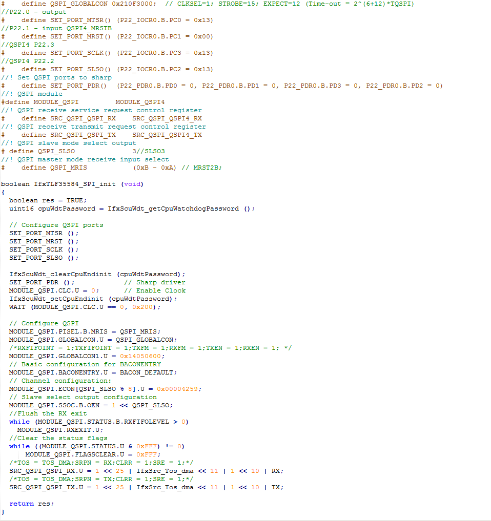
Any SPI Master with QSPI peripheral can be used for a TLF35584/TLF35585 data link. Please note that ASCLIN peripheral in SPI mode can’t be used for TLF35584/TLF35585 data link because the needed mode (idle clock low, sample on rising and shift on falling edge) is not available in ASCLIN.
- Optional: ERR – SMUFSP interface (P33.8) provides a uni-directional interface to the
TLF35584/TLF35585 safety service that is designed to react on failures detected within
the microcontroller by the integrated safety mechanisms.
P33.8 is high default state pad and push-pull when configured as SMU output. No external pull device is required for the SMUFSP interface to ensure any default state as the TLF35584/TLF35585 ERR service requires a toggling signal to indicate no error.
- Optional: INT – ESR1 provides a uni-directional interface for service requests to the
microcontroller during TLF35584/TLF35585 operation. These include various safety
pre-warnings such as over-temperature, missing or incorrect WD service and counter
increment, and ABIST step completion. Such events are not considered as critical and
therefore do not require warm or cold reset generation of the microcontroller.
ESR1 has to be configured as an input with an optional internal pull-up. No external pull-up is required at the interrupt interface. TLF35584/TLF35585 starts servicing the interrupt only after warm reset de-assertion to the microcontroller. The interrupt pulse is indicated with a low state trigger to the ESR1.
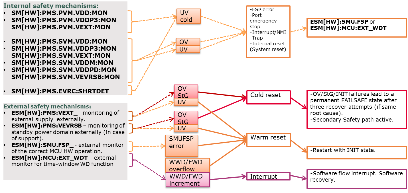
Reactions of safety mechanisms on detected faults
Reactions of the power supply sub-system on a detected fault towards the microcontroller are classified in three event types:
- NMI.
- Interrupt event.
- Warm reset and Cold reset.
| Recovery from | TLF35584/ TLF35585 state transition | Expected system reaction | System reaction time, typical | Total max time until FAILSAFE state reached (for permanent failure) | |
|---|---|---|---|---|---|
NMI/Interrupt | |||||
Non-crucial faults/soft errors. For example: Missing WD service, SPI parity error, OT warning etc. ERR signal cleared within recovery delay time etc. | Stay in same state | Trigger interrupt service routine → Readout status flag IF register → Proper system action in software flow. Write back IF register to clear | <500 µs For example: Missing WS service, program flow recovery – within close window and open window time (10 ms - 1 s) | <1 - 10 s depending on configuration | |
Warm reset class | |||||
Critical faults that do not result in overstress of the ECU components: ERR signal (recovery timeout) UV on VEXT or VEVRSB supply WWD/FWD overflow 1 - 2 missing INIT configuration on TLF35584/TLF35585 | Move to INIT state | Application software reset: Readout status flags from TLF35584/TLF35585 Check RSTSTAT.PORST = 1 || RSTSTAT.SMU = 1 (RSTSTAT.SWD = 0 & RSTSTAT.STBYR = 0) Initialize TLF35584/TLF35585 and start new safety service. Initialize application | Typ. start-up software time: <warm reset kept <2.0 ms for warm reset (with RAM init.) <1.5 ms for flash wait state configuration, PLL init and CPU clock throttling, system re-init (without PMS sub-system) etc. <4 ms Multicore start-up + Application start-up time | TLF35584/ TLF35585 default cycle time to recover from warm reset: <600 x3 ms (three consecutive attempts to recover) | |
Cold reset class (external power cycle event) | |||||
Critical faults resulting in overstress of components outside of operation condition: OV any post-regulator Short-to-ground on VEXT, VEVRSB or Pre-regulator Battery overvoltage TSD >2 missing INIT configurations on TLF35584/TLF35585 | Move to FAILSAFE state. Permanently blocked if three same consecutive failures | Application software reset as a new driving cycle: Run latent fault tests (LBIST/MBIST). Readout status flags from TLF35584/TLF35585 Run ABIST Initialize TLF35584/TLF35585 and start new safety service. Initialize application | Same as above plus: <20 ms for all failures except TSD <1 s for TSD <1 ms EVRs start-up <5 ms LBIST <5 ms MBIST <x ms TLF35584/TLF35585 ABIST | Immediately. New attempts in: <20 ms; <1 s (TSD) | |
A missing WD service, the wrong FWD answer code, or a service during a ‘Closed window’ caused by an error in program flow can be recovered within the next service cycle. Typically, recovery means that the WD error counter is decremented and no new interrupt occurs. Alternatively, an over-temperature pre-warning could mean much longer system recovery time or a limited recovery. In many cases, an over-temperature event requires a limitation of the application use case of the microcontroller in order to limit the ECU power dissipation. This could result in limited functionality, such as the vehicle driving at a moderate speed.
Reset status check after restart
TLF35584/TLF35585 reset device status flags are checked in order to trigger an appropriate restart sequence and register system event. The microcontroller will read out MONSFx, INITERR, SYSFAIL, and OTFAIL.
The RSTSTAT register of the microcontroller should be checked in addition to a TLF35584/TLF35585 status check, although it may not help to distinguish the root cause of a reset due to a concomitant power failure during a warm reset trigger from TLF35584/TLF35585 or an internal cold reset trigger.
Diagnosis of the root cause and the recovery strategy is application specific. A general solution is checking for the critical system fault that has occurred in order to identify what start-up system tests to be run, such as LBIST/MBIST. Sometimes it is not possible or practical to run all tests if there is a comparatively long restart time when operating in safety critical applications.
Example A - TLF35584/TLF35585 triggers a warm reset due to SMUFSP stop toggling operation or WWD/FWD overflow
Check TLF35584/TLF35585 flags
- SYSFAIL: No set flags. If set, another failure type like a voltage monitor status VMONSFx flags for VMONF bit is possible.
- INITERR: ERRF/FWDF/WWDF flag is set if occurred during INIT phase of TLF35584/TLF35585 state machine. If VMOF is set, check VMONSF2 flags externally for under-voltage event.
Check RSTSTAT
- RSTSTAT.PORST = 1 and/or RSTSTAT.SMU = 1.
- If RSTSTAT. EVRx = 1 and RSTSTAT-PORST=1, an internal cold reset trigger has been generated, which is potentially a root cause of the ERRF flag.
- If RSTSTAT.SWD = 1, a UV failure has occurred at the EXT/QUC supply rail. Such an event results in additional bits set in the MONSF0 and MONSF2 registers.
- If RSTSTAT.STBYR flag is set, the contents of the RSTSTAT register cannot be trusted.
Example B - TLF35584/TLF35585 triggers a cold reset (power cycle) due to thermal shutdown
Check TLF35584/TLF35585 flags
- SYSFAIL: OTF flag set.
- OTFAIL: helps to distinguish which of the integrated DTS has an error.
Check RSTSTAT
- The expectation is that no bits are set for a power cycle event of the VEVRSB domain (LVD reset).
Example C - TLF35584/TLF35585 triggers a cold reset (power cycle) due to external power failure event
Check TLF35584/TLF35585 flags
- SYSFAIL: VMONF flags set.
- Check MONSF1. If set then a power cycle event occurred.
- Check MONSF2. If UCSG/STBYSG set than a power cycle event occurred.
Check RSTSTAT
- The expectation is that no bits are set for a power cycle event of the VEVRSB domain (LVD reset).
From the examples given, the general conclusion is that a reset check starts with SYSFAIL, MONSFx, INITERR checks to understand a system state. Usually, this is followed by RSTSTAT checks.
Recommendation
If no clear source of reset can be identified from checking the status registers, any reaction that contributes to a warm reset trigger with detected RSTSTAT.SMU should be followed by SMU_ADi and AG2i_STBY checks. Alarm groups contributing to any OV event must be checked.
The safety manual highlights the types of internal error types leading to a ERR failure type (documented in the next sub-sections), which are followed by a primary reaction, warm rest class.
Safety mechanisms of the PMS sub-system with TLF35584/TLF35585
The TC3xx microcontroller provides diverse safety elements to ensure better detection of power related failures.
A split SMU structure with two independent power supplies is used for voltage related alarms. Such a structure increases the probability of a successful SMU reaction on a detected alarm if there is a failure in a core domain voltage. One part of the SMU – SMU_standby relies on the VDDPD voltage, which is isolated from the VDD voltage another SMU_core relies on. Both SMU elements are also clocked from redundant sources. For the failure modes of the core voltage or clock, the SMU_standby plays a role as back-up safety management element, which allows it to react on and maintain alarm information relevant to all supply voltages regardless of the SMU_core status.
The TLF35584/TLF35585 power supply QST keeps the PMS domain of the microcontroller alive, and therefore the SMU_standby during the warm reset generation. As shown in the previous figure, all integrated supply voltage monitors in TC3xx are maintained during VEVRSB supply. Therefore, they are kept alive during any failure recognized by the TLF35584/TLF35585 as in the warm reset class.
Power supply sub-system start-up
Early start-up flow
The diagram covers the portion of time until the cold reset of the microcontroller is de-asserted internally by the microcontroller and the supply releases the warm PORST to the microcontroller.
Start-up software flow
The figure above shows the start-up of the microcontroller after reset release. It is divided into two main parts:
- Firmware.
- User start-up software.
The following steps of user start-up software control of the power supply sub-system:
Step A
- Basic hardware configuration. Application specific board configuration for the pin configuration and EVRC.
Step B
- Enable SMU and FSP generation to external power supply unit.
Step C
- Initialize external power supply unit, initialize internal voltage monitors.
Step D
- Periodic service of the external safety monitors in post SSW phase.
- Optionally includes ABIST check of the external power supply unit.
Configuration of the TLF35584/TLF35585 system supply
Basic example configuration
The user SSW shall trigger the sequencing of following register updates:
- Read out WWD and FWD status: WWDSCMD and FWDSTAT0.
- Enable FSP-ERR pin monitoring: SYSPCFG1.
- Enable WWD and/or FWD monitors: WDCFG0.
- Configure the time window for FWD monitor: FWDCFG.
- Configure the close and open time windows for WWD: WWDCFGx.
- Service first time WWD based on read WWDSCMD: WWDSCMD.
- Service first time FWD based on read FWDSTAT0: FWDRSP and FWDRSPSYNC.
- Request transition to NORMAL state: DEVCTRL/DEVCTRLN.
- Make sure that NORMAL state transition took place: DEVSTAT.
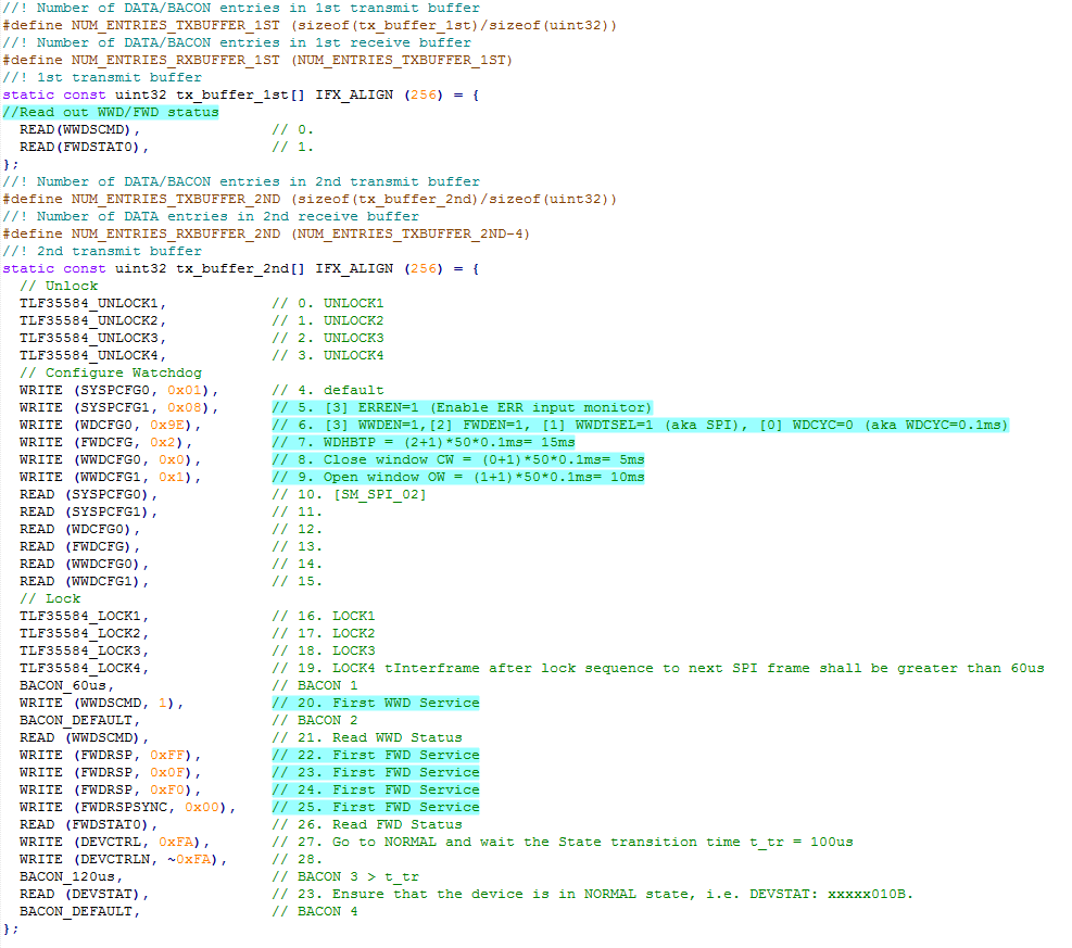
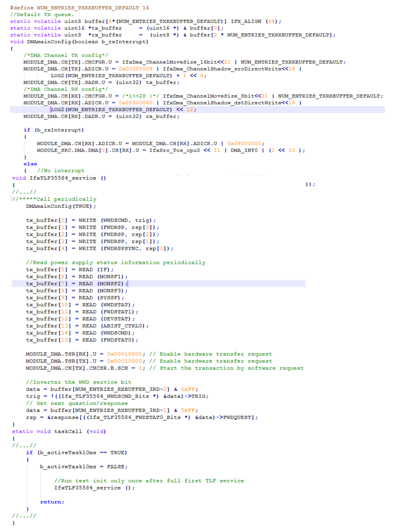
Basic example
The basic example includes SPI and DMA setup as shown. This configuration triggers the initial setup queue to the power supply and it is expected to transition in a NORMAL mode upon its successful completion. DEVSTAT register readout takes place at the end of this sequence. User software can perform a simple check if the device is in the NORMAL mode. The transmit sequence includes necessary delays implemented with BACON insertions between transmit phases of the queue.
WWD and FWD
WWD is serviced by means of an SPI command. There is also an option to service the WWD with the WDI pin interface. In the example the WWD configuration for a Closed Window of 5 ms and an Open Window of 10 ms takes place. The FWD is configured for a time window of 15 ms. These time windows are selectable in the range of 5 ms - 1600 ms.
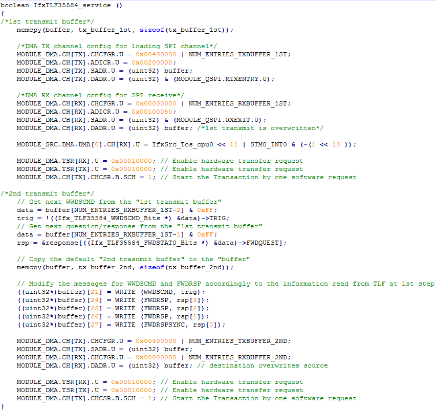
Periodic service routine
This code example shall be called periodically for the chosen power supply safety functions to be periodically serviced. The basic setup reads back the status information from the WWDSCMD and FWDSTAT0 registers, and sends an updated WWD command and FWD response during the next cycle.
SMU configuration for reaction on voltage monitors
An example SMU configuration for the interaction with TLF35584/TLF35585 and related voltage monitoring of the power sub-system includes:
- Enabling alarms for primary and secondary voltage monitors in SMU_core and SMU_stby.
- Setup of secondary voltage monitors.
- SMU reaction setup (FSPERR control).
Voltage monitoring on the system supply level
The setup of pre-warning voltage monitoring thresholds is made on consideration of voltage regulation performance described in the power supply datasheet for LDOs - QUC, QST and QVR.
For every power rail, the static accuracy region and dynamic regulation range should be taken into account in order to decide on the effective placement of monitoring thresholds. A good balance between the unavailability of the ECU function and unintended operation out of operational limits is to be found. In most of the applications, this task is difficult to perform due to the inherited inaccuracy of the voltage monitors (internal as well as external) because of the relatively narrow operating range of the microcontroller and relatively low accuracy of the voltage monitors. The over-voltage monitoring in 5V0 and 3V3 cases has only limited room to make such a configuration of Secondary Voltage Monitors (SVM).
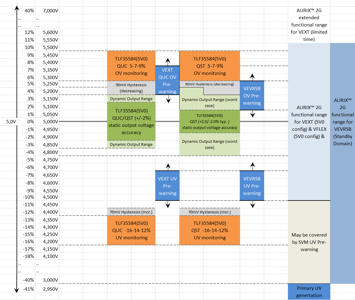
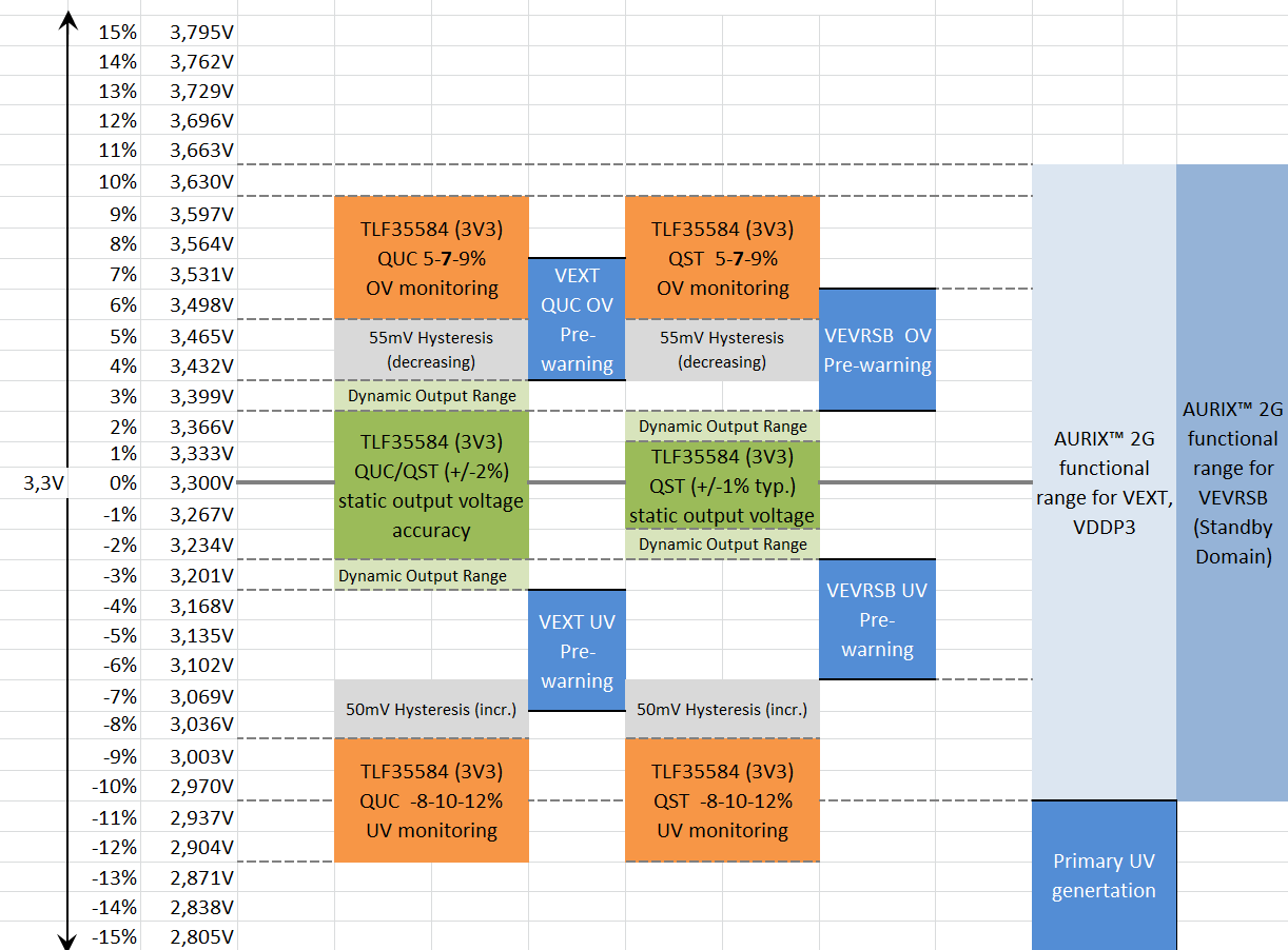
The following example shows the placement of the over-voltage threshold limits is shown with respect to the expected maximum of the dynamic regulation limits of external power rails and they are placed as close as possible to them. The under-voltage configuration in the 5V0 case has much more room for threshold placement is therefore unproblematic for a given application.
The 3V3 case has less room for under-voltage threshold placement due to the close proximity of the primary under-voltage limit for the cold reset generation. The example below shows the case where the pre-warning generation with pre-configured SVM takes place before a cold reset trigger during a negative voltage transient or a spike.
5V0 configuration
VEXT
- Over-voltage placed as close as possible to the dynamic regulation limit.
VEVRSB
- Over-voltage placed as close as possible to the static region. Immediate load current change up to 10 mA is not expected at EVRSB domain (see TLF35584/TLF35585 datasheet). The monitoring threshold placement takes dynamic regulation into account during 0...5 mA load step, which is the expected maximum.
VDDM
- Over-voltage placed as close as possible to the dynamic regulation limit.
For all domains, the under-voltage has much room for configuration options.
3V3 configuration
VEXT
- Over-voltage and under-voltage are placed as close as possible to the dynamic regulation limit.
VEVRSB
- Over-voltage and under-voltage are placed as close as possible to the dynamic regulation limit.
The following figures show example placements of voltage monitoring limits for 5 V and 3V3 system.
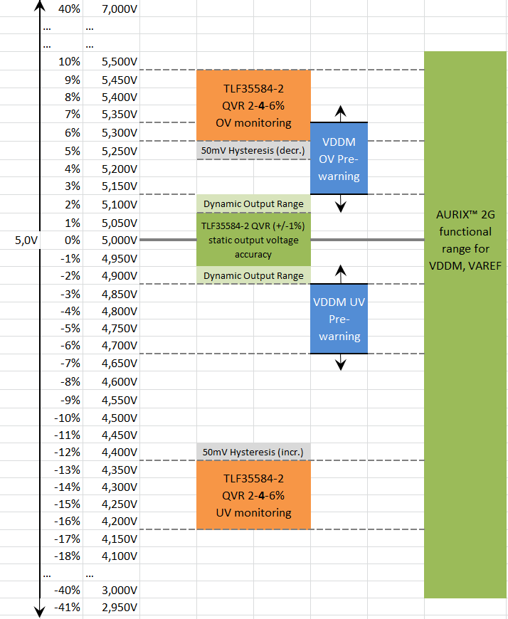
The limits in the previous diagrams are reflected in a simple register configuration of the PMS registers for EVR control. Threshold values need to be re-calculated into hex values using the equations from the TC3xx specification for SVM, as in the following example:
Example 5V0 pre-warning monitoring threshold values for under-voltage
For VDD: LSB = 5.7692 mV
- UV: at -8% - 1.15 V: Threshold = 1150/5.7692 + 1 = 0xC8;
For VDDP3: LSB = 15 mV
- UV: at -8% - 3.036 V: Threshold = 3036/15 + 1 = 0xCB;
For VEXT: LSB = 23.077 mV
- UV: at -8% - 4.6 V: Threshold = 4600/23.077 + 1 = 0xC8;
For VDDPD: LSB = 5.7692 mV
- UV: at -8% - 1.15 V: Threshold = 1150/5.7692 + 1 = 0xC8;
For VDDM: LSB = 23.077 mV
- UV: at -4% - 4.80 V: Threshold = 4800/23.077 + 1 = 0xD1;
For VEVRSB: LSB = 23.077 mV
- UV: at -8% - 4.6 V: Threshold = 4600/23.077 + 1 = 0xC8;
Example 5V0 pre-warning monitoring threshold values for over-voltage
For VDD: LSB = 5.7692 mV
- OV: at +8% - 1.35 V: Threshold = 1350/5.7692 + 1 = 0xEB;
For VDDP3: LSB = 15 mV
- OV: at +8% - 3.564 V: Threshold = 3564/15 + 1 = 0xEF;
For VEXT: LSB = 23.077 mV
- OV: at +5% - 5.25 V: Threshold = 5250/23.077 + 1 = 0xE5;
For VDDPD: LSB = 5.7692 mV
- OV: at +8% - 1.35 V: Threshold = 1350/5.7692 + 1 = 0xEB;
For VDDM: LSB = 23.077 mV
- OV: at +4% - 5.20 V: Threshold = 5200/23.077 + 1 = 0xE2;
For VEVRSB: LSB = 23.077 mV
- OV: at +3% - 5.15 V: Threshold = 5150/23.077 + 1 = 0xE0;
This data needs to be written into the EVR registers, with low-to-high and low-to-high example trigger setup for over-voltage and under-voltage pre-warning respectively:
Code listing 1 SVM example settings
void configureMonitoringThresholds(void) ( uint16 safetyWdtPassword = IfxScuWdt_getSafetyWatchdogPasswordInline (); IfxScuWdt_clearSafetyEndinit (safetyWdtPassword);
MODULE_PMS.UVMON.U = 0xC8CBC8; MODULE_PMS.UVMON2.U = 0xC8D1C8; MODULE_PMS.OVMON.U = 0xE5EFEB; MODULE_PMS.OVMON2.U = 0xE0E2EB; MODULE_PMS.MONCTRL.U = 0x00A5A5A5;
IfxScuWdt_setSafetyEndinit (safetyWdtPassword); )
SMU configuration examples
The following code example configures the SMU_core and SMU_stby to trigger a FSP reaction by the SMU_stby and a FSP reaction with System Reset class by SMU_core.
Code listing 2 SMU configuration examples
#include "IfxScuWdt.h" #include "IfxSmu_reg.h" #include "IfxPms_reg.h" #include "IfxCpu.h" #include "IfxScuWdt.h" #include "IfxSmu.h"
typedef enum ( IfxSmu_Command_start = 0,
/**< \brief Forces the SSM to go to the RUN state from the START state */
IfxSmu_Command_activateFSP = 1,
/**< \brief Activates the Fault Signaling Protocol. */
IfxSmu_Command_releaseFSP = 2,
/**< \brief Turns the FSP into the inactive fault free state */
IfxSmu_Command_activatePES = 3,
/**< \brief Triggers the activation of the Port Emergency Stop (PES). */
IfxSmu_Command_stopRT = 4,
/**< \brief Stop the recovery Timer. */
IfxSmu_Command_alarmStatusClear = 5,
/**< \brief Alarm Status Clear Enable Command */
IfxSmu_Command_triggerAlarm = 6,
/**< \brief Triggers a software based alarm */
) IfxSmu_Command;
typedef enum( extAlarmAction_FSPoff, extAlarmAction_FSPon )dm_SMUalarmActionExt;
typedef enum( intAlarmAction_noAction, intAlarmAction_reserved, intAlarmAction_IGCS0, intAlarmAction_IGCS1, intAlarmAction_IGCS2, intAlarmAction_NMI, intAlarmAction_RESET, intAlarmAction_CPU_RST )dm_SMUalarmActionInt;
typedef struct( uint16 group; uint16 num; )dm_SMUalarm;
#define ALM_GR_STBY_SMU_21 21u #define ALM_GR_STBY_SMU_20 20u #define ALM_GR_CORE_SMU_9 9u
//FSP for OV PVM through SMU_stby dm_SMUalarm dm_PVM_OValarm[] = ((ALM_GR_STBY_SMU_21,3u),(ALM_GR_STBY_SMU_21,4u),(ALM_GR_STBY_SMU_21,5u)); //RESET for OV through SMU_core dm_SMUalarm dm_OVcoreAlarm[] = ((ALM_GR_CORE_SMU_9,3u)); //FSP for UV PVM through SMU_stby dm_SMUalarm dm_PVM_UValarm[] = ((ALM_GR_STBY_SMU_21,0u),(ALM_GR_STBY_SMU_21,1u),(ALM_GR_STBY_SMU_21,2u)); //RESET for OV through SMU_core dm_SMUalarm dm_UVcoreAlarm[] = ((ALM_GR_CORE_SMU_9,5u)); //FSP for OV SVM through SMU_stby dm_SMUalarm dm_SVM_OValarm[] = ((ALM_GR_STBY_SMU_20,4u),(ALM_GR_STBY_SMU_20,5u),(ALM_GR_STBY_SMU_20,6u), (ALM_GR_STBY_SMU_20,7u),(ALM_GR_STBY_SMU_20,8u),(ALM_GR_STBY_SMU_20,9u)); //FSP for UV SVM through SMU_stby for internally generated voltages: VDD/VDDPD/VDDP3 dm_SMUalarm dm_SVM_UValarm[] = ((ALM_GR_STBY_SMU_20,10u), (ALM_GR_STBY_SMU_20,11u), (ALM_GR_STBY_SMU_20,12u)); //No FSP for UV SVM through SMU_stby for the rest of externally generated voltages dm_SMUalarm dm_SVM_VextUValarm[] = ((ALM_GR_STBY_SMU_20,13u),(ALM_GR_STBY_SMU_20,14u),(ALM_GR_STBY_SMU_20,15u));
/*Prototypes for Configuration Load functions */
void
setPMSalarmsSTBYFSP
(dm_SMUalarm
alarm
,
uint32 ui32_alarmNum
)
; void setPMSalarmsCORE(dm_SMUalarm
alarm
,
dm_SMUalarmActionInt alarmActionInt
,
dm_SMUalarmActionExt alarmActionExt
,
uint32 ui32_alarmNum
)
;
/*Load Alarm configurations */
void alarmPredefinedConfig(void) ( setPMSalarmsSTBYFSP(dm_PVM_OValarm, sizeof(dm_PVM_OValarm)/sizeof(dm_SMUalarm)); setPMSalarmsSTBYFSP(dm_PVM_UValarm, sizeof(dm_PVM_UValarm)/sizeof(dm_SMUalarm)); setPMSalarmsSTBYFSP(dm_SVM_OValarm, sizeof(dm_SVM_OValarm)/sizeof(dm_SMUalarm)); setPMSalarmsSTBYFSP(dm_SVM_UValarm, sizeof(dm_SVM_UValarm)/sizeof(dm_SMUalarm)); setPMSalarmsSTBYFSP(dm_SVM_VextUValarm, sizeof(dm_SVM_VextUValarm)/sizeof(dm_SMUalarm));
setPMSalarmsCORE(dm_OVcoreAlarm, intAlarmAction_RESET, extAlarmAction_FSPon, sizeof(dm_OVcoreAlarm)/sizeof(dm_SMUalarm)); setPMSalarmsCORE(dm_UVcoreAlarm, intAlarmAction_RESET, extAlarmAction_FSPon, sizeof(dm_UVcoreAlarm)/sizeof(dm_SMUalarm));
) /Alarm configuration for SMUstby/ void setPMSalarmsSTBYFSP(dm_SMUalarm* alarm, uint32 ui32_alarmNum) ( uint32 ui32_alarmGroupExtCF; uint32 ui32_alarmMaskCF;
uint32* ui32p_ag2xfsp_stby = &PMS_AG20FSP_STDBY;
uint16 safetyWdtPassword = IfxScuWdt_getSafetyWatchdogPasswordInline (); IfxScuWdt_clearSafetyEndinit (safetyWdtPassword);
if (alarm->group < 20u) return;
while (ui32_alarmNum) ( //Update alarm groups external ui32_alarmGroupExtCF = (extAlarmAction_FSPon & 0x01u) << alarm- >num; //Update mask ui32_alarmMaskCF = ~(0x1 << alarm->num);
SMU_KEYS.U = (uint32)0x00000bc; //Alarm group offset of 20u ui32p_ag2xfsp_stby += alarm->group - 20u;
ui32p_ag2xfsp_stby = (*ui32p_ag2xfsp_stby & ui32_alarmMaskCF) | ui32_alarmGroupExtCF | 0x40000000; SMU_KEYS.U = 0;
//return pointers to the base ui32p_ag2xfsp_stby = &PMS_AG20FSP_STDBY; alarm++; ui32_alarmNum--; ) IfxScuWdt_setSafetyEndinit (safetyWdtPassword); ) /Alarm configuration for SMUcore/ void setPMSalarmsCORE(dm_SMUalarm* alarm, dm_SMUalarmActionInt alarmActionInt, dm_SMUalarmActionExt alarmActionExt, uint32 ui32_alarmNum) ( volatile uint32 ui32_alarmGroupIntCF0; volatile uint32 ui32_alarmGroupIntCF1; volatile uint32 ui32_alarmGroupIntCF2; volatile uint32 ui32_alarmGroupExtCF; volatile uint32 ui32_alarmMaskCF;
uint32
ui32p_agxcfxPtr = &SMU_AG0CF0; uint32* ui32p_agxfspPtr = &SMU_AG0FSP;
uint16 safetyWdtPassword = IfxScuWdt_getSafetyWatchdogPasswordInline (); IfxScuWdt_clearSafetyEndinit (safetyWdtPassword);
while (ui32_alarmNum) ( //Update alarm groups internal ui32_alarmGroupIntCF0 = (alarmActionInt & 0x01u) << alarm->num; ui32_alarmGroupIntCF1 = ((alarmActionInt >> 1) & 0x01u) << alarm->num; ui32_alarmGroupIntCF2 = ((alarmActionInt >> 2) & 0x01u) << alarm->num;
//Update alarm groups external ui32_alarmGroupExtCF = (alarmActionExt & 0x01u) << alarm->num;
//Update mask ui32_alarmMaskCF = ~(0x1 << alarm->num);
SMU_KEYS.U = (uint32)0x00000bc; //CFx external ui32p_agxfspPtr += alarm->group;
ui32p_agxfspPtr = (
ui32p_agxfspPtr & ui32_alarmMaskCF) | ui32_alarmGroupExtCF; //CF0 internal ui32p_agxcfxPtr += (alarm->group
3);//Offset is x3 times
ui32p_agxcfxPtr = (
ui32p_agxcfxPtr & ui32_alarmMaskCF) | ui32_alarmGroupIntCF0; //CF1 internal ui32p_agxcfxPtr++;
ui32p_agxcfxPtr = (
ui32p_agxcfxPtr & ui32_alarmMaskCF) | ui32_alarmGroupIntCF1; //CF2 internal ui32p_agxcfxPtr++;
ui32p_agxcfxPtr = (
ui32p_agxcfxPtr & ui32_alarmMaskCF) | ui32_alarmGroupIntCF2; SMU_KEYS.U = 0;
//return pointers to the base ui32p_agxfspPtr = &SMU_AG0FSP; ui32p_agxcfxPtr = &SMU_AG0CF0; alarm++; ui32_alarmNum--; ) IfxScuWdt_setSafetyEndinit (safetyWdtPassword); ) /configure_SMU: to be called from main.c/ void configure_SMU(void) ( uint16 safetyWdtPassword = IfxScuWdt_getSafetyWatchdogPasswordInline (); uint16 cpuWdtPassword = IfxScuWdt_getCpuWatchdogPassword ();
IfxScuWdt_clearCpuEndinit (cpuWdtPassword); IfxScuWdt_clearSafetyEndinit (safetyWdtPassword);
//Configure FSP on AURIX™ error pin to service TLF35584/TLF35585 error monitoring on ERR pin. P33_PDR1.B.PD8 = 0; // set driver strength to maximum P33_IOCR8.B.PC8 = 0x10; // set output SMU_KEYS.U = 0xBC; // Unlock SMU_FSP.U = 0x3FFF << 8 | 2 << 5 | 3 << 3; // TFSP_LOW=0x3FFF (read only register); MODE=2 (time switching); PRE2=3 (100MHz/4096 = 24.4kHz) SMU_PCTL.U |= 0x85;//0x83 // PCS=1; HWDIR=1 (output);HWEN=1 (enable) SMU_KEYS.U = 0; // lock
IfxSmu_releaseFSP ();
//Configure FSP on AURIX™ on STBY side: SMUEN = 0; FSP0EN = 1; FSP1EN=0; ASCE=1; MODULE_PMS.CMD_STDBY.U = 0x4000000B;
alarmPredefinedConfig();configureMonitoringThresholds();IfxScuWdt_setCpuEndinit (cpuWdtPassword); IfxScuWdt_setSafetyEndinit (safetyWdtPassword); )
Example of TLF35584/TLF35585 configuration functions
This chapter shows that some configuration routines (such as a change of state machine mode) change the mode transition timings and current monitor threshold for wake-up for example.
The interface to the power supply is permanently used by the service function which must be executed correctly within pre-defined time windows. Other communication routines which represent asynchronous calls shall not block the interface to the power supply for longer than the selected open window and must not distort the data. The application must realize the concurrent access to the same shared resource and related infrastructure peripherals (SPI, DMA and so on) by means of resource management of a given environment (such as RTOS for example).
Code listing 3 Example of TLF35584/TLF35585 configuration functions
#include "Ifx_Types.h" #include "IfxDma.h" #include "IfxTLF35584/TLF35585_regdef.h" #include "IfxStm_reg.h"
//WKSF: attributes. Check on wake. #define TLF_STBY_FAIL_WAK 0x01u #define TLF_STBY_FAIL_ENA 0x02u #define TLF_CMON_WAK 0x04u #define TLF_TIMER_WAK 0x08u #define TLF_SPI_WAK 0x10u
//SYSSF: attributes. Check on wake. #define TLF_CUR_MON_FAIL 0x10u
//Entry attributes typedef enum ( none1, none2,//INIT. Not used TLF_GT_NORM,//NORMAL TLF_GT_SLEEP, TLF_GT_STBY, TLF_GT_WAKE, none7, none8, )t_entrySource;
//Entry delay typedef enum (//Definition of DEVCFG0.TRDEL tr_100us, tr_200us, //other values for vertical size reduction// tr_1500us, tr_1600us )t_transitionDelay;
typedef enum ( cmon_10mA, cmon_30mA, cmon_60mA, cmon_100mA ); typedef struct s_ModeTransAttr ( t_entrySource ucModeEntryAttr;//that is entry source t_transitionDelay transitionDelay;// that is stby timer uint32 ucModeExitAttr; // that is wake up flags. Check on wake event; trap in case of detected inconsistency uint32 wakeupTimeout;// that is wake-up timer
boolean cMonState;// that is cmon state if required for check uint32 cMONThreshold;//
boolean wakeUpTimerState; uint32 wakeUpTimer_10ms;
uint32 powSupActive; uint32 taskAwakeTime_10ms; struct s_ModeTransAttr
ps_NextMode; struct s_ModeTransAttr
ps_PrevMode;
)t_ModeTransAttr;
/Mode transition identifiers/ t_ModeTransAttr* p_modeBase; t_ModeTransAttr transitionStandby;
#define WRITE(cmd, data) ((((cmd) | 0x40) << 8) | ((data) & 0xFF)) #define READ(cmd) ((cmd)<<8)
#define BUFFER_SIZE_DEFAULT 16u static volatile uint16 txTLF_buffer[BUFFER_SIZE_DEFAULT] IFX_ALIGN (64); static volatile uint8 rxTLF_buffer[2*BUFFER_SIZE_DEFAULT] IFX_ALIGN (64);
volatile uint32 ui32_dmaRXcomplete_flag = 0; #define DMA_INT0 5
define TX 14
define RX 15
/DMA interrupt and flag check/ IFX_INTERRUPT (dma_raiseFlag, 0, DMA_INT0); void dma_raiseFlag (void) ( MODULE_DMA.CH[RX].CHCSR.B.CICH = 1; ui32_dmaRXcomplete_flag = 1; ) extern inline void dmaRXcompleteCheck(void) ( while (!ui32_dmaRXcomplete_flag); ui32_dmaRXcomplete_flag = 0; )
void TLFtest_initTransitionModes(void) ( //Mode to start mode test cycle p_modeBase = &transitionStandby;
transitionStandby.taskAwakeTime_10ms = TIME_1000ms; transitionStandby.powSupActive = TLF_VREF_EN | TLF_COMM_EN | TLF_TRK1_EN | TLF_TRK2_EN; transitionStandby.ucModeEntryAttr = TLF_GT_STBY; transitionStandby.transitionDelay = tr_1000us; transitionStandby.ucModeExitAttr = TLF_STBY_FAIL_WAK | TLF_STBY_FAIL_ENA |TLF_TIMER_WAK; //only single source is ok transitionStandby.cMonState = disabled; transitionStandby.wakeUpTimerState = enabled; transitionStandby.wakeUpTimer_10ms = 200u; transitionStandby.cMONThreshold = cmon_100mA; transitionStandby.ps_NextMode = &transitionSleep; transitionStandby.ps_PrevMode = NULL;
/.other modes can be initilized here./)//Shall be called from the same timer instance which is used for WWD/FWD service uint8
transmitTLF(uint32 ui32_numEntries, uint16
ui16p_TXbuffer, uint8
ui8p_RXbuffer) ( if(ui32_numEntries > 32) return ui8p_RXbuffer;
while (MODULE_DMA.TSR[RX].B.CH | MODULE_DMA.TSR[TX].B.CH);
MODULE_DMA.CH[TX].CHCFGR.U = IfxDma_ChannelMoveSize_16bit<<21 | ui32_numEntries; MODULE_DMA.CH[TX].ADICR.U = 0x00300008 | IfxDma_ChannelShadow_srcDirectWrite<<16 | LOG2(ui32_numEntries) + 1 << 8; //TODO cleanup MODULE_DMA.CH[TX].SADR.U = (uint32) ui16p_TXbuffer;
MODULE_DMA.CH[RX].CHCFGR.U = /1<<28 |/ IfxDma_ChannelMoveSize_8bit<<21 | (ui32_numEntries); MODULE_DMA.CH[RX].ADICR.U = 0x08300080 | IfxDma_ChannelShadow_dstDirectWrite<<16 | LOG2(ui32_numEntries) << 12 ; //|ui32_numEntries << 28; MODULE_DMA.CH[RX].DADR.U = (uint32) ui8p_RXbuffer;
MODULE_DMA.CH[RX].CHCSR.B.CICH = 1; MODULE_SRC.DMA.DMA[0].CH[RX].U = IfxSrc_Tos_cpu0 << 11 | 1 << 10 | DMA_INT0;
MODULE_DMA.TSR[RX].U = 0x00010000; // Enable hardware transfer request MODULE_DMA.TSR[TX].U = 0x00010000; // Enable hardware transfer request MODULE_DMA.CH[TX].CHCSR.B.SCH = 1; // Start the Transaction by one software request
//waiting routine to ensure DMA RX transaction is complete before getting RX buffer.dmaRXcompleteCheck();return ui8p_RXbuffer; )
// TLF wake-up status check uint8 TLFstateFlagRead(uint16 ui16_command) ( uint8
ui8p_RXbuffer; *txTLF_buffer = READ(ui16_command); ui8p_RXbuffer = transmitTLF(1u, txTLF_buffer, rxTLF_buffer);
return (uint8)(ui8p_RXbuffer[0]); ) /Example of wake-up time configuration/ void TLFsetModeTransitionTimes(uint32 ui32_transitionTime_100us, boolean b_wakeTimerState, uint32 ui32_wakeUpTimer_10ms) (
txTLF_buffer[0] = WRITE(DEVCFG0,(b_wakeTimerState ? (0x3 << 6) : 0 )| ((uint8)ui32_transitionTime_100us)); txTLF_buffer[1] = WRITE(WKTIMCFG0, ui32_wakeUpTimer_10ms); txTLF_buffer[2] = WRITE(WKTIMCFG1, ui32_wakeUpTimer_10ms >> 8); txTLF_buffer[3] = WRITE(WKTIMCFG2, ui32_wakeUpTimer_10ms >> 16);
transmitTLF(4u, txTLF_buffer, rxTLF_buffer); ) /Example of state transition request/ void TLFrequestStateTransition (uint32 ui32_state, uint32 ui32_enabledRegulators) ( if (ui32_state != 4u && ui32_state != 3u)//not STBY & not SLEEP ui32_state |= (ui32_enabledRegulators << 3);
txTLF_buffer[0] = WRITE (DEVCTRL, ui32_state); txTLF_buffer[1] = WRITE (DEVCTRLN, ~ui32_state);
transmitTLF(2u, txTLF_buffer, rxTLF_buffer); ) /Example of current monitor configuration/ void TLFsetCurMonThreshold(uint32 ui32_monThreshold, boolean b_cMONstate) ( txTLF_buffer[0] = WRITE(DEVCFG2,(ui32_monThreshold <= 0x3 ? ((ui32_monThreshold << 2)|(b_cMONstate << 4)) : (0x12 | (b_cMONstate << 4)) ));
transmitTLF(1u, txTLF_buffer, rxTLF_buffer); ) //call if setModeState returns TRUE; //ui32_testTimerCycle_10ms - timer cycle used as the base for running this function. void TLFtest_runModeTransitionTest(uint32 ui32_testTimerCycle_10ms) ( volatile uint8 ui8_TLFdevStatFlags = 0; ui8_TLFdevStatFlags = TLFstateFlagRead(DEVSTAT);
//increment the static variable to stay in the normal mode until the time taskAwakeTime is reached. ui32_timeCounter += ui32_testTimerCycle_10ms; if (p_modeBase->taskAwakeTime_10ms != ui32_timeCounter) return;
switch(p_modeBase->ucModeEntryAttr) ( case TLF_GT_STBY:
//Enable TLF WUT and preload the counter value if(p_modeBase->wakeUpTimerState == enabled) ( TLFsetModeTransitionTimes(p_modeBase->transitionDelay, p_modeBase->wakeUpTimerState, p_modeBase->wakeUpTimer_10ms); )
//Check if the current monitor test is required //Do not reduce micrcontroller current in such case if(p_modeBase->cMonState == enabled) ( TLFsetCurMonThreshold(p_modeBase->cMONThreshold, p_modeBase->cMonState); ) //Reduce microcontroller current otherwise //that is reduce CPU load prior the low power mode transition else ( uCconfigureStbyEntry(p_modeBase->wakeUpTimer_10ms); //TODO: preconfigure entry mechanisms that is UV entry type //- shall be preconfigured inh accordance with applicaiton requirements //TODO: preconfigure wake-up that is NMI or WUT timer or Vext ramp-up //- shall be preconfigured inh accordance with applicaiton requirements )
//Request a transition to the standby mode. //Send information about active power supplies together with mode transition information. TLFrequestStateTransition(TLF_GT_STBY, p_modeBase->powSupActive);
//Disable interrupts __disable (); //Enter stby by uC uCtriggerStbyEntry(); while(1);
break;//...//))
Other hardware aspects of TLF supplies in TC3xx applications
Output power coverage for TC3xx family
The figure below represents an overview of the power output capabilities and power consumption requirements for derivatives of TC2xx and TC3xx families.
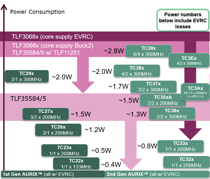
Power numbers represent MCU consumption during run mode with power patterns that are configured as Real Power Pattern with few additional modules. These patterns assume that EVR33 and EVRC are enabled and account for the power losses. The following examples show configurations for TC39x and TC35x
Code listing 4 TC39x example
Real Pattern based on Powertrain Application + few adders shown in red
TJ fixed at 150 °C
fSRI = fCPUx = 300 MHz
fGTM = 3 clusters at 200 MHz (rest at 100MHz)
fSPB = fSTM = fBAUD1 = fBAUD2 = fASCLINx = 100 MHz
VDD = 1.275 V
VDDP3 / FLEX = 3.366 V
VEXT / EVRSB / M = VDDM = 5.1 V
all cores are active including four lockstep core (3x Average IPC = 0.6
(2xLS), 3xAverage IPC = 1.2 (2xLS))
MII enabled
Dflash programming enabled
the following peripherals are inactive: HSM, HSCT, PSI5, I2C, FCE, EBU, MTU,
CIF, RIF, SPU
VADC - 12 SAR modules
DSADC – 11 modules
Code listing 5 TC35x example
Real Pattern is based on Powertrain Application
TJ fixed at 150 °C
fSRI = fCPUx = 300 MHz
fSPB = fSTM = fBAUD1 = fBAUD2 = fASCLINx = 100 MHz
fSPU = 300MHz (2 modules active with FFT at 300MHz)
VDD = 1.275 V
VDDP3 / FLEX = 3.366 V
VEXT / EVRSB / M = VDDM = 5.1 V
all cores are active: 1x Average 0.6 IPC, 2x Average 1.2 IPC + LS
HSM, RIF, MII enabled
Dflash programming enabled
the following peripherals are inactive: HSCT, PSI5, I2C, FCE, EBU, MTU, CIF
VADC - 2 SAR modules
The figure above shows that the TC39x device may approach the power limit of the TLF35584/TLF35585 supply. The limitation is dominated by the electrical and thermal limit of the QUC LDO that is used to generate the main 5 V or 3.3 V power input to the microcontroller. In order to overcome this limitation, the TLF35584/TLF35585 offers another topology with an external companion device TLF11251. This companion device enables a topology with direct pre-regulator supply to the TC3xx input for the core voltage generation.
| Type | TLF35584/TLF35585 |
|---|---|
Supply topology | Boost/Buck-PreReg Linear PostReg |
Vbatt-connected Boost (Pre-Regulator) | Y |
Vbatt-connected Buck (Pre-Regulator) | 5V8 at 1.3 A |
SMPR Buck | - |
SMPR Boost | - |
µC_LDO (PostReg) | 3V3/5 V at 600 mA |
StandBy_LDO | 3V3/5 V at 10 mA |
TLF35584/TLF35585 start-up timings
The section Start-up software flow describes start-up steps after the VEVRSB-QST supply is available (it reaches VLVDRST5 limit). The total time to reach specified triggers depends on the total start-up duration of supply LDOs.
The Pre-regulator and QST start up simultaneously after battery connection and internal reset release. The time to reach under-voltage threshold depends on the output capacitors used at each rail, the current capabilities of the regulator outputs and the total load during cold start.
TLF35584/TLF35585 offers a wide range of output capacitor selection for each system LDO. The nominal value of an output capacitor is the important external parameter to define the start-up timing of each regulator. The figure below shows examples of estimated start-up timings for few capacitor nominals and various output loads.
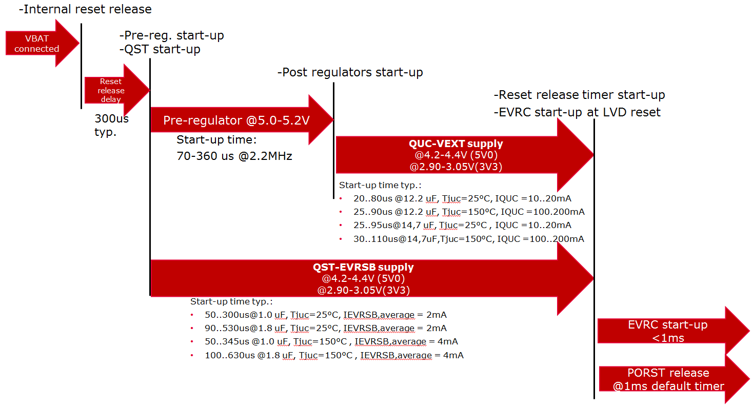
The load at the QUC output is mainly defined by the total leakage of the microcontroller during start-up. The load parameter is not a constant value and changes during the supply voltage ramp with the linear increase of the leakage and further start-up of the modules at this time. Therefore for example the EVRC starts up during LVD reset release and the QUC LDO sees this change while regulating the input voltage of the EVRC. Similarly, the QST output load changes when the PMS turns into run mode. For simplicity, such estimation assumes average load current values for various temperatures.
The rest of the start-up time variation depends on the variation of the over-current limit within the ranges specified in the TLF35584/TLF35585 datasheet. The PORST release is delayed by 1 ms by default after the regulators reach the under-voltage limits.
Revision history
| Document version | Date | Description of changes |
|---|---|---|
V1.0 | NA | Initial release |
V1.1 | 2021-09-06 | Second release All pages:
Figure 1 : PORST pull-up from 1 to 2K corrected Page 5: Description for ASCLIN corrected |
| V1.2 | 2024-03-13 | Template update; no content update. |