AN1101 FuSa in a Nutshell - Electric Vehicles main inverter application
32-bit TriCore™
AURIX™ TC3xx microcontroller
About this document
Scope and purpose
As requirements from functional safety standards in automotive, industrial and other fields are a challenging subject, this document intends to provide a first set of guidelines for users who are unfamiliar using the AURIX™ TC3xx microcontroller unit (MCU) in a functional safety scope.
This application note is part of a series of document named “FuSa in a nutshell” as listed in
3
.
Intended audience
This document is intended for all those evaluating the AURIX™ TC3xx MCU, including functional safety engineers on the customer side and application engineers. This includes designers of safety-related systems who:
Are new to functional safety
Want to know more about functional safety (also called “FuSa”) applications
Want to understand in principle how functional safety can be implemented with hardware support
Are looking for functional safety details that cannot be found in the MCU user manual
Structure of the document
This document wants to provide a first guidance on the following safety related arguments:
Main inverter system and safety considerations
Chip set for an ASIL D use case
New trends
Disclaimer
Information include in ths document are for training purposes only and are not to be taken as a blueprint for productive development.
Introduction
The most important system-level blocks of a powertrain system in an electric vehicle (EV) are the electric motor itself, the traction inverter drive, the DC/DC converter, the high-voltage Li-ion battery and the on-board charger (OBC). The traction inverter system is described in detail in the subsequent sections. This system needs to ensure that the vehicle powertrain is operating safely and at optimum efficiency.
Figure 1. Simplified block diagram of the traction inverter system
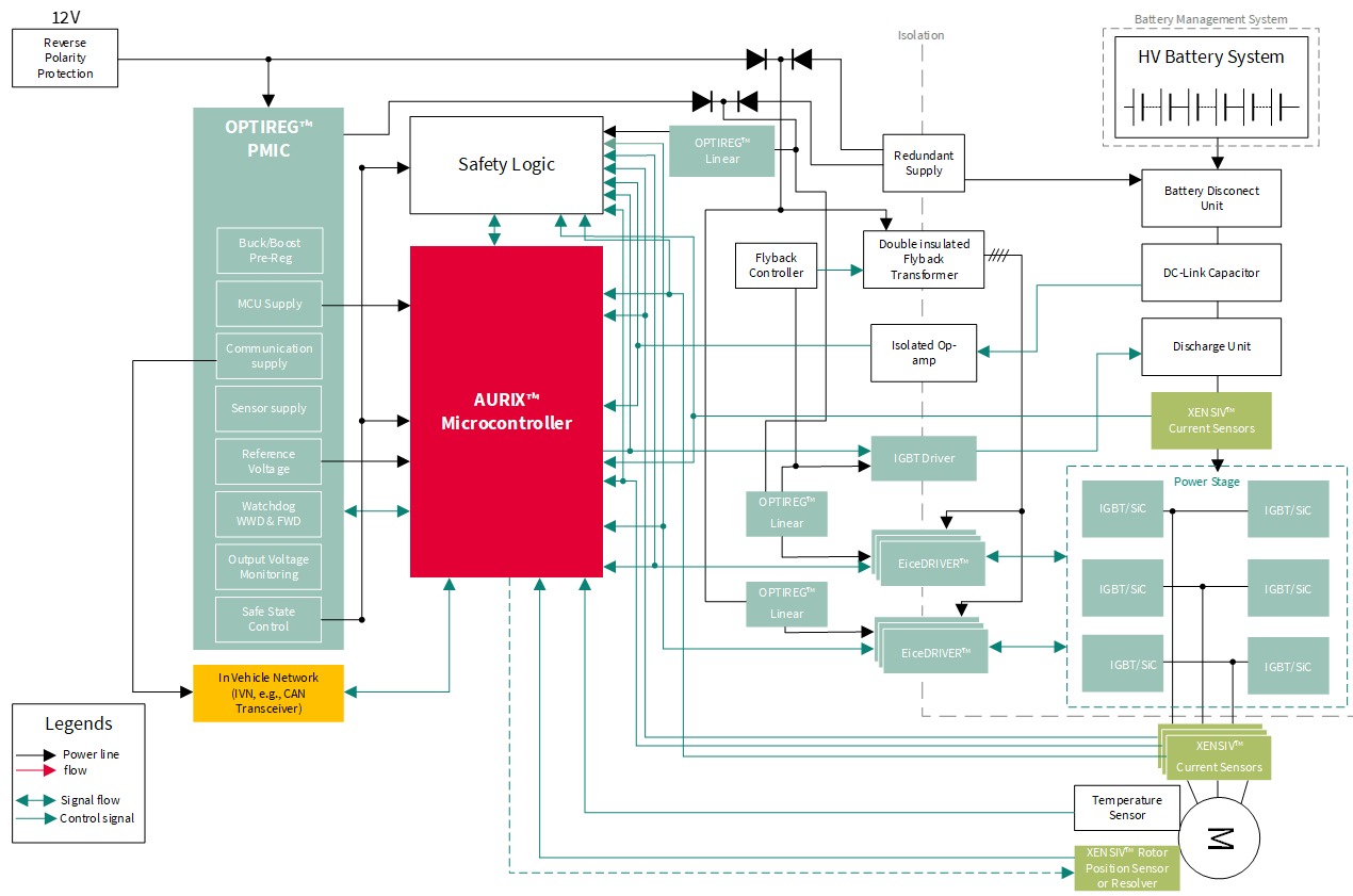
To control the traction inverter, Infineon’s AURIX™ TC3xx MCU family implements advanced features for signal acquisition with the highest safety level (multicore and lockstep architecture, DS-ADC-enabled direct resolver-to-MCU interface, customized PWM pattern generation). Surrounding the 3-phase power stage that will contain Si IGBTs or SiC MOSFETs, there are driver devices that translate the signals from the MCU and provide the necessary isolation.
To provide the multiple rails needed in a traction inverter, Infineon OPTIREG™ power management IC (PMIC) products offer integrated, multi-rail solutions specifically for the harsh automotive environment. Fast 750 V and 1200 V switching devices such as CoolSiC™ MOSFETs are best driven by galvanically isolated gate-driver ICs.
Infineon’s EiceDRIVER™ gate driver ICs incorporate the essential features necessary for driving SiC MOSFETs, such as, for example, overcurrent protection, an under- and overvoltage lockout mechanism on all supply lines and support for active short circuit and freewheeling strategies. In addition, the drivers support ASIL-D on the system level, with additional monitoring and supervision functions being integrated to simplify design for safety-relevant applications, including ISO 26262 compliance.
Current sensors in the motor phases and a position sensor on the rotor of the e-motor provide the necessary feedback for precise and energy efficient torque control of the motor, as current sensing is one of the essential measurements within a traction inverter. The Infineon XENSIV™ products offer high-precision miniature coreless magnetic current sensors for AC and DC measurements with an analog interface and fast over-current detection outputs.
Figure 2. Simplified system example of traction inverter
Most state-of-the-art electric vehicles use permanent magnet synchronous machines (PMSM) as the main electric traction motor, typically with three phases. The power range of these motors is from 20 KW up to >100 KW and they normally have 3 or 4 pole pairs with up to ≤25 krpm and a max acceleration of 115.000 rad/s2, which requires an output response of ≤ +/-0.2o for 10 krpm. Also, asynchronous e-motors are available, which have less efficiency but the same torque range respect to PMSM. They are anyway bigger and weigh more.
As the manufacturing of permanent magnets requires rare earth material and the recycling process of PMSM often results in the loss of the permanent magnets, the market share of externally excited synchronous machines (EESM) is increasing. These machines generate the magnetic field of the rotor by using copper coils, which are excited by DC current instead of permanent magnets.
Initial assumptions
To build this example, the following initial assumptions are made:
E-motor type: Permanent magnet synchronous machine (PMSM) with rare earth material
Axle propulsion is on the rear wheels of the vehicle
One central traction inverter plus an e-motor for both rear wheels (including a differential and a fixed gear)
Usually, there are two kinds of failures of the motor driver:
Open failure mode
Short circuit failure mode
Phase over-current reaction time, DC-Link overvoltage reaction time and gate driver fault reaction time are supposed to be a few microseconds (to reach a safe state), especially in context with traction inverter components protection
Other hazards that must be considered to maintain vehicle stability on the propelled wheels are considered to have a FTTI of ≤60 ms, for example, “unwanted torque” because of “wrong torque” applied to the wheels without an acceptable tolerance band
The “slow” hazards can be easily controlled by SW, while ultra-fast component protection measures usually require further HW safety countermeasures
Need for protection
The following are the safety goals when designing a traction inverter:
Avoidance of unintended high voltage (ASIL-B):
This means that the device will not generate induced voltages (acting as a generator) above 60 V without being connected to the HV battery. To fulfill this requirement, the inverter applies, for example, an active short circuit (ASC) on the low- or high-side power switches to actively clamp the motor phases, eliminating the overvoltage situation. Furthermore, an active DC-link discharge circuit is typically required to decrease the voltage in the DC-link capacitor to below 60 V in a short time (in most applications, it is 2 s). This corresponds to the time, which is considered, for example, for service staff to be able to work safely on a BEV vehicle for maintenance in a garage or in case of a vehicle crash
Avoidance of unintended torque (ASIL-D) (magnitude, direction and so on):
This means that the device will deliver the torque that is requested by the vehicle control unit (VCU) (according to a specific tolerance) with a FTTI of ≤60 ms
Avoidance of overvoltage (ASIL-B):
During normal operation, the traction inverter control and energy management ECU, between the HV-battery and main inverter, limit the maximum recovered energy that can be accepted by the battery. The traction manager receives the maximum energy limit from the BMS and translates this into a maximum permitted negative torque for the inverter. The inverter controls this by actively setting a negative torque current vector. The traction inverter is not allowed to provide uncontrolled energy flow into the battery. This is then avoided by an active short circuit at high speed or freewheeling at lower speeds
Hardware components
The major requirements and the key features of the selected components are:
AURIX™ TC3xx MCU family, the traction inverter control core
Power supply for the entire system using a PMIC and other power supply chips such as low-dropout regulators (LDO)
Gate drivers for the six IGBTs or MOSFETs (plus an additional six gate driver boosters, depending on the selected power switches)
IGBT driver for the power transistor for the active discharge unit
Rotor position measurement: To accomplish this task, magnetic xMR angle sensors or a resolver can be used. The acquired data is transmitted to the MCU via CAN (UART). If a resolver is used, the AURIX™ TC3xx family provides support for resolver-to-digital conversion (RDC)
Current measurement for every AC phase of the motor and optionally, also for the DC current from or to the battery
CAN (-FD) Transceiver for communication with the vehicle
Temperature sensors: For example, eMotor-, power module-, PCB- and coolant- temperature
DC-link voltage sensing
AURIX™ TC3xx MCU
To control the traction inverter, Infineon’s AURIX™ TC3xx MCU family offers up to hexa-core performance and advanced features for signal acquisition and pattern generation, connectivity, security and functional safety, ensuring it is ideally suited for many automotive applications, including traction inverter control. Through a closed-loop control scheme, the AURIX™ TC3xx MCU supports the exact torque and speed control of the traction motor. AURIX™ TC3xx can supply many features.
The following are the various timer modules available:
Concatenated advanced timer outputs (ATOMs) + dead time modules (DTMs) for PWM generation, including an adjustable dead time
Dead time module (DTM) shut-off path with TIM input for fast switch-off
CCU6 input for PWM pattern verification
The CCU6 module is not always applied for redundant acquisition or actuation. The choices are multiple and depend on the system integrator’s preference. The same applies for the rotor sensor, which can be plausibly checked by MCU internal rotor position estimators.
Angle and speed feedbacks are often reconstructed by diverse additional observers (for example, Kalman filters) to double-check the function of the primary rotor position sensors. This kind of safety solution allows for ASIL-D supervision for the vital rotor position and speed feedback and inputs for the field-oriented motor control algorithm.
MCU power supply
The power management IC device can manage and monitor the various power supplies of a complex MCU. One important functional safety feature of this integrated circuit should be its ability to detect and report faults in the power supply, such as overvoltage, undervoltage and overcurrent conditions. The device includes a range of built-in protection mechanisms, such as voltage and current clamping, to help preventing damage to sensitive electronic components in the event of a fault.
The power supply circuit should also include several features to help ensure reliable and stable power delivery to critical vehicle systems, including multiple regulated outputs, each of which can be programmed to a specific voltage and current limit. Another relevant safety feature is the presence of a time-window watchdog to monitor the system for malfunctions and automatically reset the device if the MCU is not responding in the right manner.
Additionally, the MCU power supply can request a safe state (independently from the MCU) if it is assumed that the MCU is not working properly. This is a redundant safety path. In addition to its functional safety features, a good power supply integrated circuit is designed to be highly efficient and reliable. The device should be capable of operating at high temperatures (the ambient temperature is often defined in a range between -40°C and 85°C) and include advanced thermal protection features to prevent damage from overheating.
Figure 3. Infineon TLF35584 safety connections of the power supply module (besides needed supplies)
provides an example of connections needed for functional and safety purposes when using the TLF35584 PMIC as a power supply chip. As Infineon is permanently expanding the portfolio with dedicated chips and solutions, check the company website or the regional support for the newest chipset.
Besides the power supply of the AURIX™, the power supply IC also has a supervision function for the microcontroller. During operation, the MCU and the power supply IC are exchanging signal patterns to check if the MCU is still in the right operation and is trustworthy. If the power supply IC is receiving the wrong pattern several times, an MCU power removal can be forced as a safe reaction.
If the MCU cannot be assumed to be trustworthy for executing the right PWM pattern and actions, the power supply IC uses its SS1 and SS2 pins to force the inverter into a safe state (either with active short circuit or freewheeling) without having to rely on the MCU’s functionality. This redundant safety path is a basic need to enable an ASIL-compliant design.
NR | AURIX™ | PMIC | Description |
|---|---|---|---|
1-4 | SPI- pins | SPI- Pins | SPI data transmission for configuration and data readout in a bidirectional way |
5 | FSP | ERR | Diagnostic output signal from AURIX™ TC3xx to TLF to activate an independent safety path |
6 | ESR1 | INT | Safety output from PMIC to AURIX™ |
7 | PORTX.Y | WDI | Watchdog input signal from AURIX™ |
8 | PORST | ROT | Reset to AURIX™ |
9 | PORTA.B | SS1 | For the startup test of SS1 output effectiveness (optional) |
10 | PORTC.D | SS2 | For the startup test of SS2 output effectiveness (optional) |
Gate drivers
Infineon provides an advanced single-channel IGBT driver that can also be used for driving power MOS devices. The device’s aim is to optimize the design of high-performance safety-relevant automotive systems. The gate driver used in this example is based on Infineon's coreless transformer technology and consists of two chips separated by galvanic isolation. The low-voltage (primary) side can be connected to a standard 5 V logic. The high-voltage (secondary) side is in the HV-battery domain.
Internally, data transfers are ensured by two independent communication channels. One channel is dedicated to transferring the ON and OFF information of the PWM input signal only. This channel is unidirectional (from the primary-low voltage side to the secondary high-voltage side). As this channel is dedicated to PWM information, latency time and PWM distortion are optimized. The second channel is bidirectional and is used for other data transfers (status information, error handling and other functions).
The device supports advanced functions to optimize the switching behavior of the power switches. Furthermore, it supports several monitoring and protection functions, making it suitable for systems that must fulfill ASIL requirements (as per ISO 26262).
The gate driver IC incorporates a serial peripheral interface (SPI) for communication with an external MCU, allowing for bidirectional data exchange and enabling the configuration and control of the gate driver IC. This interface facilitates seamless integration into the overall system and enhances flexibility in driving IGBTs or MOSFETs. In addition, the gate driver IC also features a pulse width modulation (PWM) input. The PWM input enables precise control of the gate driver output signals by accepting pulse width-modulated signals.
Furthermore, the gate driver IC includes fault output pins NFLTA and NFLTB. These pins provide fault status information to the inverter system. When a fault condition, such as overtemperature (of the internal circuitry of the gate driver) or undervoltage lockout, is detected, the NFLTA or NFLTB pins (according to the type of fault) are triggered to indicate the fault condition. This enables the system to promptly respond to fault events, implement appropriate protective measures and ensure functional safety.
As a bridge short circuit (current flowing from HV+ to HV- because the HS- switch and the LS- switch are conducting at the same time) has the highest priority to be avoided, several measures ensure it. At first, the AURIX™ TC3xx is adding sufficient deadtime in between the PWMs for HS and LS to avoid a cross-conduction or shoot-through. If this measure fails, as there is, for example, a single failure on the PCB level, both gate drivers (HS and LS) supervise each other (through INP and INSTP connections) and will not let the opponent gate driver switch on if it is still conducting. Even if this fails, the DESAT detection of the gate driver will recognize the too-high cross-current and turn off the switch. This is an example of how the Infineon chipset ensures a reliable and ASIL-compliant implementation.
Figure 4. Infineon 1EDI2002AS - EiceDRIVER™ and gate driver booster connection schematics
To evaluate the impact of the described functionality on the system in terms of required pins, the Infineon 1EDI2002AS - EiceDRIVER™ is considered as the described IC.
needs to be repeated six times for the six IGBTs or MOSFETs to consider the correct pinout of AURIX™ TC3xx.
NR | AURIX™ | Gate driver | Description |
|---|---|---|---|
1 | GPIO | NFLTA | Fault A output (low-active, open drain). Goes to AURIX™ GPIO as input. This should be combined with the other two EiceDRIVER™ signals on the high side or low side. |
2 | GPIO | NFLTB | Fault B output (low-active, open drain). Goes to AURIX™ GPIO as input. This should be combined with the other two EiceDRIVER™ signals on the high side or low side. |
3 | GTM-(A)TOM | INP | PWM input comes from the GTM timer output module (ATOM or TOM channel). It needs to be connected to the INSTP pin on the other side of the “leg”. |
4 | INSTP | Signal that provides shoot-through protection (STP) to the system. It needs to be connected to the INP pin on the other side of the “leg”. | |
5 | GPIO | EN | Enable input. It comes from an AURIX™ GPIO output pin. This should be combined with the other two EiceDRIVER™ signals on the high side or low side. |
6 | VSS | REF0 | The signals INP, INSTP and EN are pseudo-differential in the sense that they are not referenced to the common ground GND1 but to the REF0 signal. This is intended to make the device more robust against ground-bouncing effects. |
7 | GPIO | NRST/RDY | Reset input (low-active, open drain). This signal notifies the AURIX™ GPIO input that the device is “ready”. This should be combined with the other two EiceDRIVER™ signals on the high side or low side. |
8-11 | SPI-pins | SPI-Pins | SPI data transmission for configuration and data readout in a bidirectional way. Daisy chain with the other five SPIs of other EiceDRIVER™. |
When it comes to the combination of six EiceDRIVER™, for both functional safety and hardware protection, it is sufficient, in most cases, to group (OR combination) the faults (faults by NFLTA pin and faults by NFLTB pin) in high-side faults and low-side faults. This results in the following four signals:
High-side fault A
Low-side fault A
High-side fault B
Low-side fault B
Gate driver booster
In high-power applications, such as traction inverters for electric vehicles, the gate driver booster often uses the downstream gate driver to ensure efficient and reliable operation of the power semiconductors, typically insulated gate bipolar transistors (IGBTs) or metal-oxide-semiconductor field-effect transistors (MOSFETs).
A gate driver booster is necessary in the following scenarios:
Faster switching speed:
Power semiconductors in high-power applications often operate at high switching frequencies. The gate driver booster is designed to provide faster rise and fall times for the gate voltage, allowing the power semiconductors to switch on and off quickly. This capability minimizes switching losses and improves overall system efficiency
Driving large gate capacitances:
Power semiconductors, particularly those used in high-power applications, have relatively large gate capacitances. The gate driver booster is designed with sufficient current-driving capability to charge and discharge these capacitors quickly. This ensures efficient switching and minimizes the risk of voltage overshoots or insufficient gate voltage during operation
Improved system robustness:
High-power applications often face challenging operating conditions, such as high temperatures, voltage transients and voltage spikes. The gate driver booster enhances the robustness of the gate driving circuit by providing adequate voltage and current reserves, improving the system's ability to handle such demanding conditions
Compatibility with high-voltage supplies:
In traction inverters and other high-power applications, the power supply voltages can be quite high. The gate driver booster is designed to operate efficiently with these high-voltage supplies, ensuring reliable performance and maintaining the necessary voltage levels for gate driving
Increased redundancy and additional shut-off path:
By adding the booster IC, an important safety feature can be used. As, without the booster, the only shut-off path is just “through” the gate driver, the booster enables direct active short circuit (ASC) functionality, including the possibility of by-passing the gate driver (the ASC pin of the booster)
This integrated circuit is not connected directly to the MCU but instead is cascaded after the gate drivers, so no AURIX™ TC3xx dedicated ports and pins are needed to command this integrated circuit. The integrated circuit taken as a reference for this example is the Infineon 1EBN1001AE - EiceDRIVER™ Boost, which is usually paired with the gate driver described earlier. When using the ASC functionality, one can benefit from the matched chipset. If the ASC pin is triggered externally, the same signal can be connected to the output stage disable (OSD) pin of the gate driver (see
Figure 5
). The problem is that if an ASC is activated without the gate driver itself enabling it, the gate driver output (TON, TOFF) and the ASC logic can work against each other, which may lead to an unsafe state. Using this connection, the OSD pin of the gate driver sets the gate driver output to “high impedance” and the booster can act as it should without any interference from the gate driver. Normally, the connection is implemented on the low-side boosters. It is important to explain the need for an external ASC feature. As discussed in Section
MCU power supply
, the MCU supply IC (PMIC TLF35584) is supervising the AURIX™ TC3xx MCU. If any malfunction of the MCU is detected, the supply IC triggers its SS outputs. These outputs can be connected (in combination with additional logic) to this ASC function to enable an ASC on the inverter level, which is not dependent on the functionality of the MCU itself or even on the functionality of the gate driver. This ensures high redundancy and diversity, resulting in a low FIT-rate shut-off path. This feature is not needed in all use cases, but it can be applied when a high ASIL rating is required.
Figure 5. Gate driver and 1EBN1001AE - EiceDRIVER™ booster connections
Rotor position - resolver
Resolvers are absolute-angle transducers that are mounted on the motor shaft to get the motor’s absolute angular position. Resolvers are often used for angle sensing in noisy environments because of their rugged construction and their ability to reject common-mode noise.
Resolver applications, as shown in
Figure 6
, determine the rotation angle by evaluating the induced signals from two orthogonally placed coils, SIN and COS. These coils are excited by the magnetic field of a third coil (EXC). Their amplitudes are modulated with the sine and cosine magnitudes corresponding to the current resolver position.
Figure 6. Resolver system representation
AURIX™ TC3xx family provides support for resolver-to-digital converters (RDC) by providing the following functionalities:
Carrier generation
(EDSADC hardware)
EDSADC hardware supports the generation of resolver excitation carriers by providing PWM pin outputs that can be filtered by a low-pass filter circuit to obtain a pair of differential signals
Signal acquisition and carrier cancellation
(using EDSADC hardware)
Two differential signals are generated from a resolver device (Sin+, Sin-, Cos+, Cos-). These signals can basically be connected directly to the two channels of EDSADC, where each EDSADC channel has P and N inputs
Timestamp acquisition
(using GTM TIM hardware)
Typically, the user's application runs at a different sampling rate than the EDSADC output sampling rate. For example, the motor control PWM interrupt occurs with 10 kHz sampling, whereas the EDSADC interrupt runs with ~9.7 kHz. This condition creates a situation where the sampled resolver position is already aged with a few timer ticks, but this can be significant to the motor control algorithm.
Therefore, a timestamp, which indicates the elapsed time since the last EDSADC channel sampling, is required for compensating or computing the missing rotor position. In addition, this timestamp is also used to compensate for the group delay, which is an inherent property of EDSADC
To implement this functionality into the system, no additional integrated circuits are needed; only the power stages for the S5 and S6 signals and a few other usual passive components are required.
NR | AURIX™ | Resolver | Description |
|---|---|---|---|
1 | DSADC0 | S1 | DS channel x input |
2 | DSADC0 | S2 | DS channel x input |
3 | DSADC1 | S3 | DS channel y input is in a different cluster with respect to S1, S2. It is not necessary to have a different GPIO port, but it is recommended unless you can detect a CCF with a plausibility check. |
4 | DSADC1 | S4 | DS channel y input |
5 | DSADC2 | S5 | Carrier generation |
6 | DSADC2 | S6 | Carrier generation |
In this example, redundant measurements could be considered. Using system properties to do a plausibility check on the sine and cosine values requires a good knowledge of the system. In the scope of this document, it can be simpler to duplicate channels using enhanced delta sigma ADC (DSADC) or enhanced ADC (EVADCs) for the sensor feedback.
Furthermore, the excitation signal (also known as the carrier generator signal), which delivers a known data sequence, should be read back with an EVADC or EDSADC channel by the MCU.
In addition, there are other common-cause failures in ADC modules; for example, the analog voltage reference (
V
REF
) requires a dedicated safety check that allows to deduce unintended drift of the analog signal conversion. Here, multiple solutions are feasible, such as using a redundant second
V
REF
, which can be compared to the main one or the internal bandgaps of the MCU itself.
It is important to make the following general considerations about resolvers:
As a Safety Element out of Context (SEooC), AURIX™ TC3xx safety concept will require DSADC redundancy for each analog acquisition.
In the context of resolver measurement, the physical properties of the coils’ relationship are well known; consequently, plausibility checks between signals are possible and can be used for safety purposes. Examples of signal properties well known are:
Zero crossing twice per period with a 90° phase shift
sin2 + cos2 = 1
Relationships between signals as listed above can be very strong to fulfill ASIL rating requirements when accompanied by timestamp acquisition and a robust plausibility check. The decision of which is the best solution for the specific resolver should be taken by the system engineer who is in charge of all the system aspects.
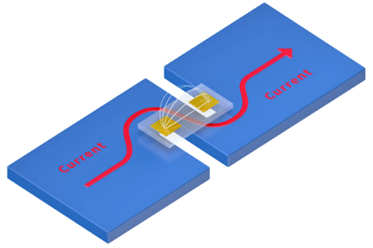
Current measurement
The current sensor from Infineon is a highly reliable and functionally safe solution designed for accurate current measurement. It offers a range of features to ensure safety and precise operation.
Figure 7. Current sensing example: Lateral sensor insertion
The sensor is equipped with two independent fast over-current detection (OCD) pins, enabling efficient monitoring and protection against excessive current levels. These pins provide an additional layer of safety by allowing the system to quickly respond and mitigate potential risks associated with overcurrent conditions, which are programmable by the customer for specific thresholds and deglitch timings. The OCD pins are designed as open-drain outputs and can be connected to the logic input pins of the MCU and/or the pre-driver to quickly react to over-current events. The OCD1 pins can be easily setup in a wired-OR configuration to monitor several current sensor outputs via only one MCU pin.
The advantage of the additional OCD2 pin is the low latency in the detection of positive and negative overcurrents. Depending on the primary current slope and the programmed threshold, detection latencies of about 1 us can be implemented with the Infineon current sensor. This enables fast hardware protection. OCD2 pins from different sensors should not be connected together if diagnosis mode is enabled (default). In this case, the OCD2 fault indication of one sensor may unintentionally activate the diagnosis mode on the other sensors by forcing the pin to ground.
Another notable feature is the configurable analog output operational mode. It offers flexibility in selecting the operational mode, whether fully differential or single-ended. This adaptability enables seamless integration into different system architectures, catering to specific application requirements and optimizing overall performance.
Figure 8. Application circuit for TLE4972 current sensor, fully differential and single-ended
The current sensor combines precise current measurement, independent overcurrent detection pins, configurable operational modes and a a robust design compliant to functional safety rating (ISO 26262 ASIL B).
To evaluate the pin requirements of the system implementing the current sensing functionality, the Infineon TLE4972 is considered a reference.
shows connections with three current sensors, included in the pin count for differential mode connection.
NR | AURIX™ | Current Sensor | Description |
|---|---|---|---|
1 | DSADC0 | V REF Sensor x | Reference voltage I/O, analog output signal in fully differential mode, synchronized with ATOMs PWM pattern to the gate driver input to AURIX™ TC3xx delta sigma ADC module |
2 | DSADC0 | AOUT Sensor x | Analog output signal (for TLE4972): Input to AURIX™ TC3xx delta sigma ADC module |
3 | GPIO | OCD1 Sensor x-y-z | Over-current detection output 1 (open drain output) Wired OR of all OCD1 pins of the three current sensors |
4 | GPIO | OCD2 Sensor x | Over-current detection output 2 (open drain output) of current sensor x |
5 | DSADC1 | V REF Sensor y | Reference voltage I/O, analog output signal in fully differential mode, synchronized with ATOMs PWM pattern to the gate driver input to AURIX™ TC3xx delta sigma ADC module |
6 | DSADC1 | AOUT Sensor y | Analog output signal (for TLE4972): Input to AURIX™ TC3xx delta sigma ADC module |
7 | GPIO | OCD2 Sensor y | Over-current detection output 2 (open drain output) of current sensor y |
8 | DSADC2 | V REF Sensor z | Reference voltage I/O, analog output signal in fully differential mode, synchronized with ATOMs PWM pattern to the gate driver input to AURIX™ TC3xx delta sigma ADC module |
9 | DSADC2 | AOUT Sensor z | Analog output signal (for TLE4972): Input to AURIX™ TC3xx delta sigma ADC module |
10 | GPIO | OCD2 Sensor z | Over-current detection output 2 (open drain output) of current sensor z |
In addition, the current sensor depicted on top of the power stage in
Figure 1
is optional and usually found in most complex inverters. The control of the inverter is fully doable without the mentioned current sensor, but it gives additional information that may be used for plausibility checks, for example, power comparisons between the AC and DC sides. The power at the DC side can also be calculated using the voltage measured at the DC-link capacitor.
It is important to make the following general considerations about current measurements:
As a Safety Element out of Context (SEooC), the AURIX™ TC3xx safety concept will require ADC redundancy for analog acquisition
In a 3-phase current measurement context, the physical properties of the current signals are well-known; consequently, plausibility checks on AURIX™ TC3xx between signals are possible. Examples of signal properties well known are:
Zero crossing twice per period with a 120° phase shift
IA + IB + IC = 0
The PWM pattern is well known, so it is possible to know which currents are physically possible
The above-listed plausibility checks are useful to develop a good safety solution.
Other common-cause failures in ADC modules should be considered; for example, the analog voltage reference (
V
REF
) requires a dedicated safety check that allows for the detection of unintended drift. Here, multiple solutions are feasible, such as using a redundant second
V
REF
, which can be compared to the main one or the internal bandgaps of the MCU itself.
As the current sensors are individual sensors, they can also be supplied with different supply voltages to ensure a redundancy in supply if requested by the safety requirements. Further things to be checked from a safety perspective include, for example, broken wire detection. An indication of typical failure modes to be considered in an analog acquisition can be found in the MCU safety manual provided under the non-disclosure agreement (NDA).
Temperature sensor
The temperature sensor is often implemented as an analog device specifically designed for accurately measuring the temperature of a board component or system part, enabling further safety monitoring and control. This is not a mandatory safety measure but is commonly used to check that the working temperature range of the system is not exceeded.
One important factor is accuracy, which should be maintained across a wide temperature range, allowing for effective monitoring in both extreme hot and cold conditions. The sensor's output represents the temperature being sensed, enabling easy interpretation and integration with existing systems.
To perform out-of-range detection within the AURIX™ TC3xx, the temperature sensor, its supply and the circuitry around it must be designed to ensure normal operation between 0.5 V and 4.5 V at the ADC pin of the AURIX™ TC3xx. This enables monitoring to determine if the signal is within this range or outside. If it is outside the range, a wire may be broken or the supply may be missing. This is important to verify the plausibility of the measured temperature value. As for the purpose of this example the temperature is a “complementary” measure; it is therefore not considered redundant.
NR | AURIX™ | Temperature sensor | Description |
|---|---|---|---|
1 | VADC | Vout | Voltage output for temperature value |
Note: AURIX™TC3xx also offers die temperature sensors (DTS), which can be used from a safety concept perspective as a complementary source of input to perform plausibility checks.
CAN transceiver
To make the inverter integrated within the entire car system, an integrated circuit that accomplishes CAN communication is needed. For this reason, a CAN transceiver must be selected to enable the AURIX™ TC3xx MCU to communicate using that specific bus protocol.
Some of the key features of a good CAN module are:
Fail-safe features such as TxD time-out, RxD recessive clamping and overtemperature shut-down, that allow the system to perform in a predictable manner in a safety-critical situation. Other safety measures also report the CAN short circuit proof to ground, battery and VCC, as well as undervoltage detection on the supply voltages
Local failure diagnostics should also be implemented by specifically designed output pins
Keeping into account the earlier mentioned characteristics of a CAN transceiver, the Infineon TLE9252V CAN transceiver is taken as a reference to understand how the CAN functionality can be integrated into the safe system itself.
Figure 9. TLE9252V CAN transceiver connections with MCU and power supply
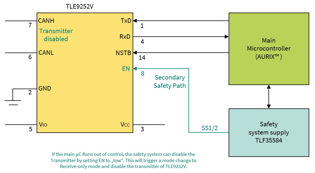
Referring to
Figure 9
, the connection required with the MCU is reported in
Table 6
.
NR | AURIX™ | CAN TR. | Description |
|---|---|---|---|
1 | CAN | TxD | Transmit data input from the MCU |
2 | CAN | RxD | Receive data output to the MCU |
3 | GPIO | NSTB | Stand-by control input (for the transceiver) |
IGBT driver for active discharge unit
In an active-discharge-unit application for inverters, the IGBT plays a critical role in managing the discharge process effectively and safely. It is specifically designed to handle the controlled and gradual release of energy from the inverter's capacitors or energy storage devices.
One of the notable features of this IC is its capability to provide a fast discharge path. It facilitates rapid and efficient energy release from the capacitors, aiding in reducing the residual voltage within a short span of time (in most cases, 2 s).
To ensure the safe operation of the system, the IC incorporates various protection mechanisms. It includes features such as overcurrent protection, overvoltage protection and thermal protection. These safeguards prevent any potential damage or overheating during the discharge process, thereby enhancing the safety and reliability of the inverter system.
The IC also offers a control interface that enables seamless integration with the overall inverter control system. It allows external control signals to initiate or halt the discharge process, facilitating coordinated operation and control over the energy discharge.
Figure 10. Infineon AUIRS212 IGBT driver connection scheme
In summary, the IC used in the active discharge unit application for inverters, enables safe and controlled discharge of energy from the inverter's capacitors or energy storage devices. The reference taken for this use case is the Infineon AUIRS212.
NR | AURIX™ | IGBT driver | Description |
|---|---|---|---|
1 | GPIO | IN | Logic input for gate driver from the MCU |
2 | GPIO | FAULT | Indicates an over-current shutdown has occurred, signal going to the MCU |
DC-link voltage sensing
In a traction inverter, the DC-link voltage can be sensed using a delta-sigma modulator and a digital isolator. A voltage divider reduces the actual DC-Link voltage to an analog signal (-1 V to 1 V), which is then converted into a bitstream. The clock (for example, 10 MHz) to synchronize the delta-sigma modulator and the MCU can be sent out by the AURIX™ TC3xx itself to avoid another clock generator. This digitalized voltage is processed within the control system for closed-loop control, fault detection and protection purposes, providing accurate sensing with electrical isolation.
Figure 11. Voltage sensing connection
As per
Table 8
, three pins are required for the MCU in the system.
NR | AURIX™ | DC-link voltage | Description |
|---|---|---|---|
1 | GPIO | STAT | indicator output from external chip to MCU |
2 | EDSADC clock | CLK | Modulator clock output from EDSADC of MCU to the external modulator |
3 | EDSADC | OUT | External modulator data output from external chip to the MCU EDSADC |
Power management and redundant supply
The power supply concept of a main inverter with redundant supply from a 12 V chassis battery and from an HV battery is mandatory to maintain under all circumstances the safe state of a traction inverter. There are basically two main supply sources, handled by a fly-back controller and a transformer.
In this system, the “continuous supply” concept is implemented, which means that it does not matter whether the supply comes from the high voltage or not. Basically, if one supply fails, the redundant one will still allow the system to run and the safety logic to handle the situation as intended.
When two diodes are placed in opposite directions, as shown in
Figure 12
, it is possible to find a redundancy node where there is an “OR” between the low voltage supply and the high voltage supply, coming from the redundant supply. What is between the two diodes (the power supply branches going to the flyback transformer and to IGBT’s) go into the flyback transformer to ensure galvanic isolation and a different number of windings for the secondary side to get a higher voltage level for the secondary side of the gate drivers with respect to the primary side. On the secondary side, there will be at least four lines, of which three are dedicated to the high-side gate drivers for the H-bridge and one for all low sides.
Figure 12. Redundant supply representation
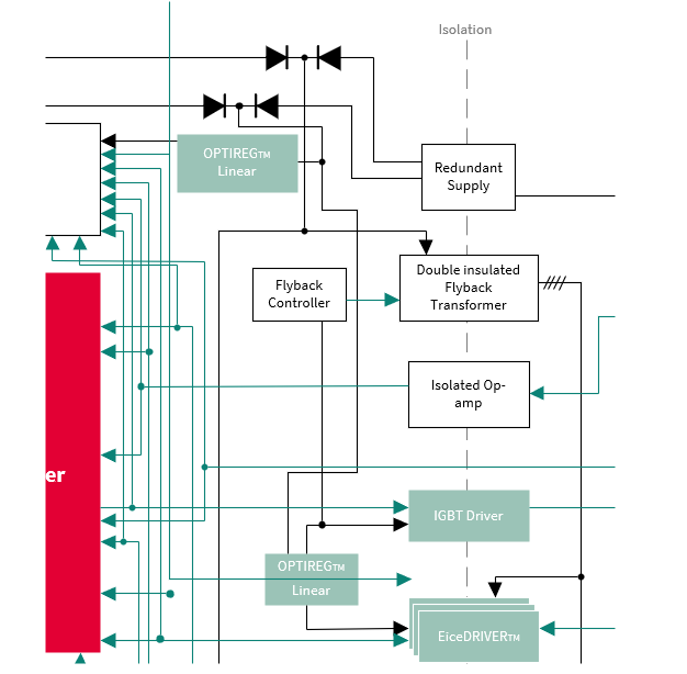
The reason why the system needs a separate voltage for each high-side gate driver is that the imposed voltage into the gate is related to a floating voltage reference (phase voltage); instead, on the low side, the reference voltage is the minus pole or negative terminal of the battery. Power lines in some systems can be six, one for each gate driver, especially for fast-switching SiC applications. There are many other possibilities to implement a redundant supply; the one depicted here is reported as an example.
Safety considerations - inverter safety logic
For the inverter use case, cars can have either front wheel drive or rear-wheel drive. This can cause some serious issues since applying the wrong torque to the rear side of a car makes the vehicle’s dynamics change dramatically and it is easy to lose control of the vehicle. The car makers focus on what happens when the motor is failing and on controlling how it fails, since the severity of the fault is high. The safety logic unit is not inside the MCU but is physically separated. This block is a redundant logic on the system level that supervises signals and can react independently.
In a few inverter applications, the safety logic will be a complex programmable logic device (CPLD) or a field programmable gate array (FPGA); in other applications, it can be a second MCU that handles small tasks such as phase overcurrent monitoring, overvoltage and safe state switching. Note that a second MCU also must maintain, under all circumstances, the permissible FTTI safety limits; therefore, software tasks may face the same limitations as on the main MCU.
For inverter applications, the inverter cannot detach itself from the wheels as it can be for an EPS system, but the battery can. For example, in the case of braking using the electric motor for energy recuperation, the inverter will inject a lot of energy into the high-voltage (HV) grid of the system if the HV battery is not fully loaded yet. See
Figure 13
to understand the entire power flow diagram, including the recuperation phase.
Figure 13. Power flow diagram for a two eAxle electric vehicle (EV)
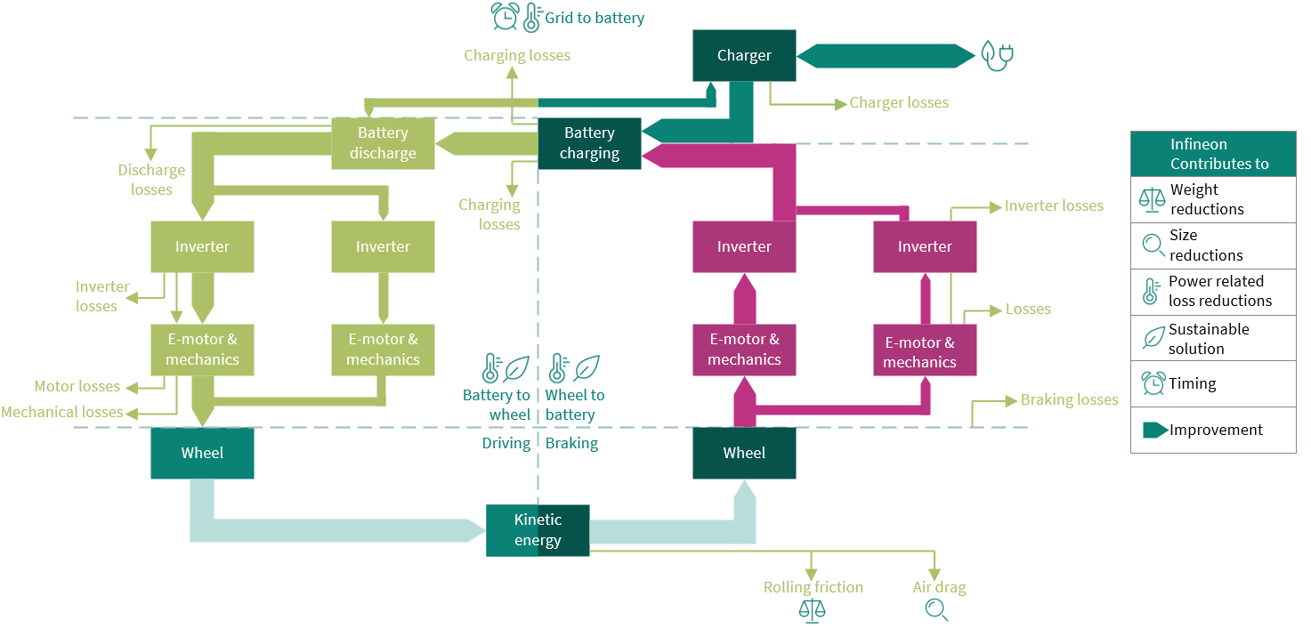
In case the battery is disconnected during the recuperation phase (deceleration), this can cause some serious damage to the circuits as the inverter cannot “push” the current to the battery. Therefore, the inverter must react within hundreds of microseconds to avoid destructive overvoltage. This happens, especially if the motor goes into the “field weakening” mode, because the motor can feedback to the inverter voltages that are higher than the maximum withstand voltage (>1200 V) of the components inside the inverter.
For this reason, the “safety logic” integrated circuit must make sure that the inverter triggers an ASC to the traction motor, clamping the voltage to zero either on only the high side or alternatively on only the low-side IGBT drivers, to not generate back electromotive force (EMF) when the electric motor is turning. Nevertheless, in dependence of the traction motor type (for example, PMSM), this state may not be allowed in certain lower rpm ranges (for example, below rated PMSM motor speed), as here the generated negative brake torque may lead to locking the propulsion wheel(s) and by this risking vehicle safety again. For this situation, free-wheeling (all switches open) may be the better choice, as long as the generated voltage to the IGBTs does not exceed the maximum electrical IGBT break-through voltage.
As can be easily seen from the example discussed in this section, a safe state of a traction inverter may consist of not only one single reaction of the system but also of a combination of multiple states depending on the application environment.
Trends
Further integration trends, such as combining an on-board charger (OBC) with the inverter and reusing the motor stator windings of the PMSM for grid charging, will add additional requirements to the MCU, such as isolation supervision versus grid and enlarged operating hours because of the added time for charging.
Autonomous driving vehicles can require redundant inverter electronics and 6-phase e-motors (2x3 phases). This does not change the ASIL-related requirements for the single-inverter electronics themselves.
References
Infineon Technologies AG:
AURIX™ TC3xx User’s Manual
; 81726 Munich; 2021-02; Available online
Infineon Technologies AG:
TriCore™ TC1.6.2 core architecture manual
; Available online
Infineon Technologies AG:
AN1000
- FuSa in a Nutshell - release note
; Available online
Glossary
Definition | Description | Notes |
|---|---|---|
ASC | Active Short Circuit | in the Inverter Use Case |
Architectural Element | The smallest element on which the FMEDA is performed | |
ASIL | Automotive Safety Integrity Level; refer to ISO 26262-1:2018, 3.6 | |
BEV | Battery-powered Electric Vehicle | |
CCF | Common-Cause Failure; refer to ISO 26262-1:2018, 3.18 | |
DC | Diagnostic Coverage; refer to ISO 26262-1:2018, 3.33 | |
DFA | Dependent Failure Analysis identifies single events that can cause multiple sub-parts to malfunction (for example, intended function and its safety mechanism) and lead to a violation of a safety requirement or safety goal. | |
DMI | Data Memory Interface | |
DPF | Dual-Point Failure; for the definition refer to ISO 26262-1:2018, clause 3.38 | |
DSPR | Data Scratch Pad RAM | |
ECU | Electronic Control Unit | |
FHTI | Fault Handling Time Interval is defined in ISO 26262 as the sum of three elements: The fault detection time, the fault reaction time and the time for the system to reach a safe state. | |
FTTI | Fault Tolerant Time Interval; for the definition refer to ISO 26262-1:2018, clause 3.61 | |
FMEA | Failure Mode and Effects Analysis | |
FMEDA | Failure Modes, Effects and Diagnostic Analysis Analysis of the effect of random hardware faults on a safety requirement or safety goal, including quantitative estimation of failure rates and the probability/rate of a safety goal violation | Quantitative Bottom-up HW only |
FTA | Fault Tree Analysis Analysis in which a top-level failure mode is broken down to a combination of lower-level faults (root causes) using a Boolean logic approach | Qualitative (may be quantitative) Top-down HW only |
HARA | Hazard Analysis and Risk Assessment; Refer to ISO 26262-1:2018, 3.76 | |
HW | Hardware | |
IC | Integrated Circuit | |
IEC | International Electrotechnical Commission | |
ISO | International Organization for Standardization | |
LBIST | Logic Built-in Self Test | |
LMU | Local Bus Memory Unit | |
MCU | Microcontroller unit | |
MMIC | Monolithic Microwave Integrated Circuit is a type of integrated circuit (IC) device that operates at microwave frequencies (300 MHz to 300 GHz). These devices typically perform functions such as microwave mixing, power amplification, low-noise amplification and high-frequency switching. | |
PMI | Program Memory Interface | |
PMIC | Power Management ICs (PMICs) | |
PMSM | Permanent Magnet Synchronous Machine (with rare earth material) | Motor type |
PSPR | Program Scratch Pad RAM | |
Safety Flip Flops (SFF’s) | Safety flip-flops are special flip-flops that implement a hardware mechanism capable of detecting bit flips within the protected registers, thus preventing single-point faults. | |
Safety Measure | Activity or technical solution to prevent, detect, control or mitigate systematic and random failures. | |
SBC | system basis chips (SBC) SBCs combine mainly three functionalities in a single device: Power supply, CAN and/or LIN transceivers and supporting features (MCU supervision, SPI interface and so on). This integration makes SBC a potentially better alternative to standalone (discrete) solutions, especially in terms of total solution cost and total area. | |
SE | Soft Error | |
SM | Safety Mechanism: for the definition refer to ISO 26262-1:2018, 3.142 | |
SW | Software | |
SPU | Signal Processing Unit | |
STP | Shoot-Through Protection: Protection typical of an inverter gate driver so that the high side and the low side of the three-phase motor legs cannot be activated simultaneously | |
VCU | Vehicle Control Unit |
Revision history
Document revision | Date | Description of changes |
|---|---|---|
V1.0 | 2024-09-12 | Initial release |
V1.1 | 2025-06-11 | Template update Updated the title |