AN0001 AURIX™ TC3xx functional safety (FUSA) in a nutshell
32-bit TriCore™
AURIX™ TC3xx microcontroller
About this document
Scope and purpose
As requirements from functional safety standards in automotive, industrial and other fields are a challenging subject, this document intends to provide a first set of guidelines for users who are unfamiliar using the AURIX™ TC3xx microcontroller unit (MCU) in a functional safety scope.
Intended audience
This application note is intended for all those evaluating the AURIX™ TC3xx MCU, including functional safety engineers on the customer side and application engineers. This includes designers of safety-related systems who:
Are new to functional safety
Want to know more about functional safety (also called “FUSA”) applications
Want to understand in principle how functional safety can be implemented with hardware support
Are looking for functional safety details that cannot be found in the MCU user manual
Structure of the document
This document is divided into four main sections:
Section
Introduction to main safety concepts
, Section
AURIX™ TC3xx products platform and scalability
, and Section
Introduction to FUSA application
are introductory sections to the AURIX™ TC3xx platform, functional safety and first steps in this complex world
Section
AURIX™ TC3xx MCU and FUSA
presents the structure of AURIX™ TC3xx and how safety is built within
Section
ISO 26262 - Electric power steering
and Section
ISO 26262 - XEV traction inverter
discuss application use cases with AURIX™ TC3xx and its interoperability with other Infineon-suitable chips
Section
Safety software enablement and AURIX™ TC3xx
explains how safety software fits with AURIX™ TC3xx built-in features
Disclaimer
Sections about application use cases (Section
ISO 26262 - Electric power steering
and Section
ISO 26262 - XEV traction inverter
) are for training purposes only and are not to be taken as a blueprint for developing such units.
Introduction to main safety concepts
To explain how to proceed when facing functional safety aspects using AURIX™ TC3xx, the following sections provide a brief introduction to basic safety concepts.
Functional safety
Functional safety defines an entire domain of modern industrial activities. In general, safety is used in relation to situations that can cause harm to humans or generally, the risk of physical injury or damage to the overall health of people (that is, a safe system will not cause harm to humans). In general, no system can be created completely safe, so the functional safety domain focuses on reducing the risk of harm to an acceptable level. The acceptable level is society-dependent and can be differently evaluated depending on the social context.
Functional safety is described as follows:
In the umbrella standard (IEC 61508:2010):
As part of the overall safety that relates to the following:
Equipment under control (EUC)
Control system of the EUC that depends on the correct functioning of the Electric/Electronic/Programmable (E/E/PE) safety-related systems
Other risk reduction measures
In the automotive standard (ISO 26262:2018):
Absence of unreasonable risk due to hazards caused by the malfunctioning behavior of E/E systems.
The electronic components are clearly mentioned in the above two definitions; therefore, this domain is relevant to semiconductors.
The functional safety process starts with a hazard analysis and risk assessment (HARA) of the relevant system or subsystem by suitably qualified and experienced personnel.
From the analysis and assessment, individual safety goals are defined with the specific objective of avoiding harm during an operational condition of the vehicle/appliance or of the automated action in general.
To each of these goals, a corresponding safety integrity level (SIL) as specified in the umbrella standard IEC 61508 is assigned based upon the risk evaluation. In the automotive domain, the acceptable risk level is called Automotive Safety Integrity Level (ASIL).
From the system level, the safety goals are translated into safety requirements for subsystems and individual hardware components. Once the design is complete, verification is carried out by a combination of the component manufacturer and the system manufacturer following the 'V'-model.
Systematic and random faults
Faults in a functional safety system can be broadly classified into the following two categories:
Systematic faults: A fault in design or manufacturing that can be present in hardware and software. The existence of systematic faults can be reduced through continual and rigorous process improvement and robust analysis of any new technology or component
Random faults: A fault of a hardware element that follows a probabilistic distribution. Random faults are limited to hardware. The rate of random faults cannot be reduced. It is important to keep the focus on:
Prevention measures such as process and design (for example, layout rules)
Detection and mitigation by safety mechanisms (for example, ECC, redundant data storage)
Figure 1. Faults classification
Random hardware faults can be permanent or transient. If the fault is permanent, it will stay there over time.
In case where errors are transient, they can be removed by writing or resetting or setting a new value. In
Figure 2
, it is possible to find a simplified representation of the major cause of transient faults in semiconductors. Alpha and neutron particles cause transient faults that need to be considered when determining the failure rate of a chip.
Figure 2. Alpha particles and neutron particles as possible causes of transient failures
ISO 26262 and IEC 61508 standards perspective
AURIX™ TC3xx was initially developed for automotive systems and is compliant with the ISO 26262:2018 standard. At the same time, compliance with IEC 61508:2010 was also assessed.
summarizes the main differences between the two standards relating to their applicability to AURIX™ TC3xx.
Section | ISO 26262 | IEC 61508 |
|---|---|---|
Application field | 12-part standard that is strictly for on-road vehicles, such as passenger cars, trucks, buses and motorcycles, covering the concept up to the production stage for electrical/electronic systems. This standard is tailored to the needs of the automotive industry. Originated from IEC 61508 for automotive. | 7-part industrial-related standard; most often used for machinery, oil wells, chemical plants, nuclear sites, forklifts and robots. This standard refers to industrially relevant technical standards for EMC, communication and cybersecurity. |
Safety classification | Classification is based on Automotive Safety Integrity Levels (ASIL). ASIL: A (least stringent), B, C, D (most stringent) | Classification is based on Safety Integrity Level (SIL). SIL: 1 (least critical), 2, 3, 4 (most critical) |
Functional Safety | definition is in ISO 26262-1:2018 clause 3.67 | definition is in IEC 61508-4:2010 clause 3.1.12 |
Areas covered | it covers safety management, system/HW design, SW design, production and operation of safety-critical E/E/PE systems, but the same is valid for components. | Covers safety management, system/HW design, SW design, production and operation of safety-critical E/E/PE systems. |
“Components” view | Automotive systems distinguish system design from hardware component design. “Components” used in the system require specific compliance with the ISO 26262 standard. One life cycle for all (tailoring concept). ISO 26262-11 is specific for semiconductor development. | A hardware component compliant with IEC 61508 is called a “compliant item”. The HW component life cycle is introduced for “ASICs”. ISO 61508-2 Annex E and F are for semiconductors. |
How safety is implemented | The safety goal concept requires risk reduction to be a part of the initial control system design. | The safety function concept was initially based on the idea of defining equipment under control (EUC) and then building risk reduction measures for the system. |
Documentation | ISO 26262 clearly defines work products for each requirement. Confirmation reviews with independent reviewers, dependent on ASIL, are requested. | General considerations on documentation are reported in Part 1, Clause 5. No confirmation reviews are requested; only assessments with independent assessors. Relating documents to be provided, there are less detailed requirements (no WPs). |
SIL and ASIL determination | To determine the ASIL level of a system, a risk assessment must be performed for all hazards identified. Risk comprises three components: severity, exposure and controllability. | The SIL level of a product is determined by three factors: Systematic capability rating : If the quality management system meets the requirements of IEC 61508, a SIL capability rating is issued. Architectural constraints for the
element : Architectural constraints are established by Route 1H or Route 2H. Route 1H involves calculating the Safe Failure Fraction for the element. PFH (or PFDavg) calculation for the
product : PFH is the average frequency of a dangerous failure of the safety function [h-1] for high demand mode of operation or continuous mode of operation, while PFDavg is the average probability of a dangerous failure on demand of the safety function operating in low demand mode of operation. |
Corresponding terms | Item Defined in ISO 26262-1:2018 respectively at clause 3.41 | Functional unit Defined in IEC 61508-4:2010 respectively at clause 3.4.5 |
Corresponding terms | Element, Fault, Failure Defined in ISO 26262-1:2018 respectively at clause 3.41, clause 3.54 and clause 3.50 | Element, Fault, Failure Defined in IEC 61508-4:2010 respectively at clause 3.4.5, clause 3.6.1 and clause 3.6.4 |
Decomposition versus synthesis | ASIL decomposition is defined in ISO 26262-1:2018 clause 3.3 An ASIL D safety requirement can be decomposed as: ASIL D (D) + ASIL QM (D) or ASIL C (D) + ASIL A (D) or ASIL B (D) + ASIL B (D) | According to IEC 61508-2:2010, SIL synthesis essentially allows the synthesis (or combining) of two redundant elements with a systematic capability of ‘N’ to have a systematic capability of ‘N + 1’, with ‘N’ less than or equal to SIL 3. The rules for SIL synthesis according to IEC 61508 are:
The IEC 61508 standard does not allow recursive SIL synthesis and in addition, the two combined elements should have the same SIL. IEC 61508 also requires a two-channel implementation for SIL 4 systems (the hardware fault tolerance has to be >0 for a SIL 4 function). |
Failure rate (λ) Expressed in FIT (see Failure rate ) | λ = λ SPF + λ RF + λ MPF + λ S | λ = λ S + λ D = (λ SD + λ SU ) + (λ DD + λ DU ) |
Definitions for the different component of failure rate | λ SPF – Single-point faults λ RF – Residual faults λ MPFDP – Detected/perceived multi-point faults λ MPFL – Latent multi-point faults λ MPF = λ MPFDP + λ MPFL – Multi-point faults λ S – Safe faults Expressed in FIT | λ S – Safe failure rate: No impact on safety function λ SD – Safe detected failure rate − λ SU – Safe undetected failure rate • λ D – Dangerous failure rate − Impact on safety function − λ DD – Dangerous detected failure rate − λ DU – Dangerous undetected failure rate Expressed in FIT |
Metrics | In automotive systems, metric targets are mandatory on the item level and are related to both single- and multi-point faults. | In IEC 61508 metrics, the most relevant factors are single-point faults, even if they include common cause evaluation through a β factor. |
Probabilistic metrics | Probabilistic Metric for Random
Hardware Failures (PMHF): Quantitative criteria for the residual risk of a safety goal violation due to random hardware failures. In simple terms: A metric to show the robustness of a safety architecture. P MHF = λ SPF + λ RF + 0,5 × λ SM1, DPF, latent × λ IF, DPF × T lifetime Expressed in FIT | In an architecture without
redundancy (1oo1) PFH = λ DU PFH definition is in IEC 61508-4:2010 clause 3.6.19 Expressed in FIT |
Similar metrics terms | Single Point Fault Metric
(SPFM): Quantitative criteria for the effectiveness of the safety architecture to cope with single-point and residual faults. In simple terms, metric for the share of remaining dangerous faults in relation to all faults. Expressed in percentage | Safe Failure Fraction (SFF): Ratio of safe and dangerous (but detected) failures in a system safety function to the total failure rate. SFF exact definition is in IEC 61508-4:2010 clause 3.6.15 SFF is calculated at the element (component) or system level for a safety function. It should not be applied to sub-elements. Expressed in percentage |
Metrics terms unique to ISO | Latent Fault Metric
(LFM): Quantitative criteria for the effectiveness of the safety architecture to cope with latent dual-point faults.In simple terms: A metric for the share of remaining critical latent faults in relation to all dual-point faults. Expressed in percentage | |
Terms unique to IEC | Low-demand mode safety functions are required to operate at low frequencies, typically once or more per year. Low-demand functions have less stringent requirements on PFDavg (the average probability of a dangerous failure on demand of the safety function) to achieve a specific SIL. High-demand mode safety functions are required to operate at high frequencies, typically many times per hour. High demand and continuous demand functions have more stringent requirements on PFH (average frequency of a dangerous failure of the safety function) to achieve a specific SIL. Continuous-demand mode safety functions operate continuously. For more details refer to IEC 61508-4:2010 clause3.5.16 Type A products are simple products in which all failure modes are known. For more details refer to IEC 61508-2:2010 clause 7.4.4.1.2. Type B products are complex products in which not all failure modes are known (for example, semiconductor). For more details refer to IEC 61508-2:2010 clause 7.4.4.1.3. Hardware Fault Tolerance
(HFT) HFT is the number of faults that can occur without failure of the safety function. A hardware fault tolerance of N means that N+1 is the minimum number of faults that can cause a loss of the safety function. For more details refer to IEC 61508-2:2010 clause 7.4.4.1. For AURIX™ TC3xx, HFT is equal to 0. This means that the fault might be detected, but safety functionality is lost with one fault. With a hardware fault tolerance of 0 (in other words, 1oo1 redundancy), the maximum safety integrity level that can be achieved by a Type B (complex semiconductor) safety-related element is SIL 3. HFT > 0 requires redundancy. | |
Fault Tree Analysis | A Fault Tree Analysis or equivalent top-down analysis is required in the case of ASIL C and ASIL D. | A Fault Tree Analysis or equivalent is only “R” (recommended) in IEC 61508. |
Dependent Failure Analysis | DFA is the analysis to identify single events that can cause multiple sub-parts to malfunction (for example, intended function and its safety mechanism) and lead to a violation of a safety requirement or safety goal. DFA is qualitative in automotive standard. | DFA is quantitative and faults in the diagnostic circuit can contribute to FMEDA metrics with the so-called beta factor. |
Safety Element out of Context (SEooC) in automotive
AURIX™ TC3xx is an MCU developed for various applications.
Since it is not tailored for a specific item, according to automotive safety standard ISO 26262 part 10, the AURIX™ TC3xx is a Safety Element out of Context (SEooC) hardware component.
As ISO 26262-10:2018 highlights, the development of an MCU starts with an assumption of system-level attributes and requirements. It is the responsibility of the system integrator to integrate the SEooC assumptions of use.
According to the ISO 26262 classification, the MCU is a hardware component that performs a set of functions at the item level as a part of a system. A system, as it is defined in ISO 26262-1, is composed of at least three related elements: a sensor, a controller and an actuator.
Figure 3
shows the typical use of the AURIX™ TC3xx in the context of an electronic control unit (ECU).
Inputs are provided by one or more sensors at the system level, processed by the HW components on the ECU and forwarded to the input channels of the MCU
The MCU processes the data and provides outputs to other hardware components
Hardware components drive one or multiple actuators or transmit data to another ECU via a communication network
Figure 3. AURIX™ TC3xx in the context of an electronic control unit (ECU)
Fail-safe system
A system is said to be fail-safe if it is designed such that in the event of a failure of any element of the system, the system prevents harm to humans.
This is accomplished by having the system enter a safe state if any safety-relevant failure occurs or if it detects a “latent” failure that cannot be corrected immediately.
Failure rate
Failure rate is the frequency or rate with which a system or component fails, expressed in failures per hour.
Symbol: λ(lambda)
Unit: 1 FIT = 10
-9
h
-1
(failure in time)
Failure rates scale depending on time and the number of systems or components.
Examples of different meanings of 1 FIT:
If there are 10
9
systems or components, one of them will fail every hour.
or
If there are 10
5
systems or components working 10
4
hours consecutively, one of them will fail.
Fault-related timings
ISO 26262 perspective
One of the key metrics for a functional safety system is the time to reach a safe state after a fault occurs.
This period, known as the Fault Handling Time Interval (FHTI), is the sum of two elements:
Fault detection time (FDTI)
Fault reaction time (FRTI)
A more commonly used term, similar to FHTI, is the Fault Tolerant Time Interval (FTTI) , which is defined in ISO 26262-1:2018 clause 3.61 and provides the minimum time before a system could become dangerous when a fault occurs.
shows a graphical representation of the relationship between these timings.
Figure 4. Fault Tolerant Time Interval
The worst case for the fault detection time is application-specific and defined by the diagnostic time interval. All hardware safety mechanisms within AURIX™ TC3xx hardware provide a very fast fault detection time, in the order of microseconds.
IEC 61508 perspective
A term corresponding to FTTI in the IEC 61508 standard is the “process safety time”. This time is defined in IEC 61508-4:2010 at clause 3.6.20. In general, the time to react to a fault is longer in industrial applications with respect to automotive ones.
Protective measures
When the need for a protective measure is identified and the classification is determined, the measure must be implemented in the system.
Safety systems can have various principles of operation, for example:
One single device is inherently fail-safe (so without integrated primary or secondary protection)
One single device with periodic self-testing and monitoring, where the control layer and primary and secondary protection layers are integrated into one single device
Two independent devices are compared using the same or different technology Secondary protection is provided by the comparison
Single device, inherently fail-safe
Electronic fail-safe devices can include fuses, circuit breakers or current-limiting circuits, which interrupt electrical currents under overload conditions. As a result, they directly prevent damage to wiring or circuit devices.
Single device with periodic self-testing and monitoring
One of the most common safety architectures is what some industrial standards call a "single device with periodic self-testing and monitoring". In this architecture, protective measures can be implemented in a number of layers, as shown in
Figure 5
.
Figure 5. Layers of safety systems in the case of a single device with periodic self-testing and monitoring
Safety-classified functionalities that will lead directly to a hazard are implemented through a control layer plus a primary and secondary protection layer. This means that the system needs to be safe even when two independent faults occur.
The worst case is when two faults happen, one in the control layer and another in the primary protection layer, at a time distance that depends on the acceptable risk for the system (normally 12–24 hours in the most restrictive case). Statistically, it is considered that there is a very low probability that more than two independent faults occur.
The functional layer is intended as the component necessary for the control tasks such as receiving signals from sensors and sending control signals to actuators. This is referred to as the “control layer”. In the absence of any protective measures, failures in combination with normal conditions in the control layer can directly lead to a hazardous situation, such as sending a spurious control signal to operate a valve. Such failures are considered "critical failures".
A second layer is necessary to implement safety measures to detect critical failures. These measures can be considered as forming the second functional layer (primary protection), whose task is to initiate a protective action in the event of a critical failure in combination with all defined “normal conditions”.
Faults that remain without leading to a critical failure are considered latent faults. Latent fault diagnostics can be executed with a lower frequency with respect to faults leading to safety-critical failures. This kind of fault, normally occurring in the protective function, nevertheless leads to a hazardous situation, even years later, in combination with a second fault.
It will be necessary to incorporate safety measures that prevent such a situation. To prevent a dropout of primary protection due to a latent fault, the proper functioning of the "safeguards" is supervised. The necessary function can be considered a third functional layer (secondary protection).
By implementing primary and secondary protection layers, a function with a high safety rating can be realized.
Two independent channels with comparison
Figure 6. Layers of a safety system using two devices with comparison
When adopting the technique of two independent channels with comparison, these two can use the same or different technology targeting the same function. In other terms, it includes homogeneous redundancy or redundancy with diversity.
When applying diversity to a system, it is not necessary to use hardware components from different manufacturers; the goals can also be achieved by using components from a single manufacturer.
This approach is limited to detecting that there is a fault but not determining where the fault is, as opposed to redundant systems with higher number of instances where the majority of voters will determine which channel is faulty (this is, for example, the case of at least two channels giving the same information over three channels present).
The final layer of protection is then provided by the comparator. The comparator itself will be guaranteed in its functionality; therefore, tests need to be run on the comparator to detect faults leading directly to a hazard or to cover latent faults. The comparator itself should also be free from systematic faults as per the rest of the system.
AURIX™ TC3xx products platform and scalability
Infineon’s AURIX™ TC3xx family concept offers both scalable feature sets and scalable pinouts for optimal flexibility, as well as requirements meeting up to ASIL-D and SIL 3 classified requirements. Depending on the specific application and its functional safety system requirements, users can choose the product that best fits to their specific case.
Figure 7.AURIX™ TC3xx scalability table
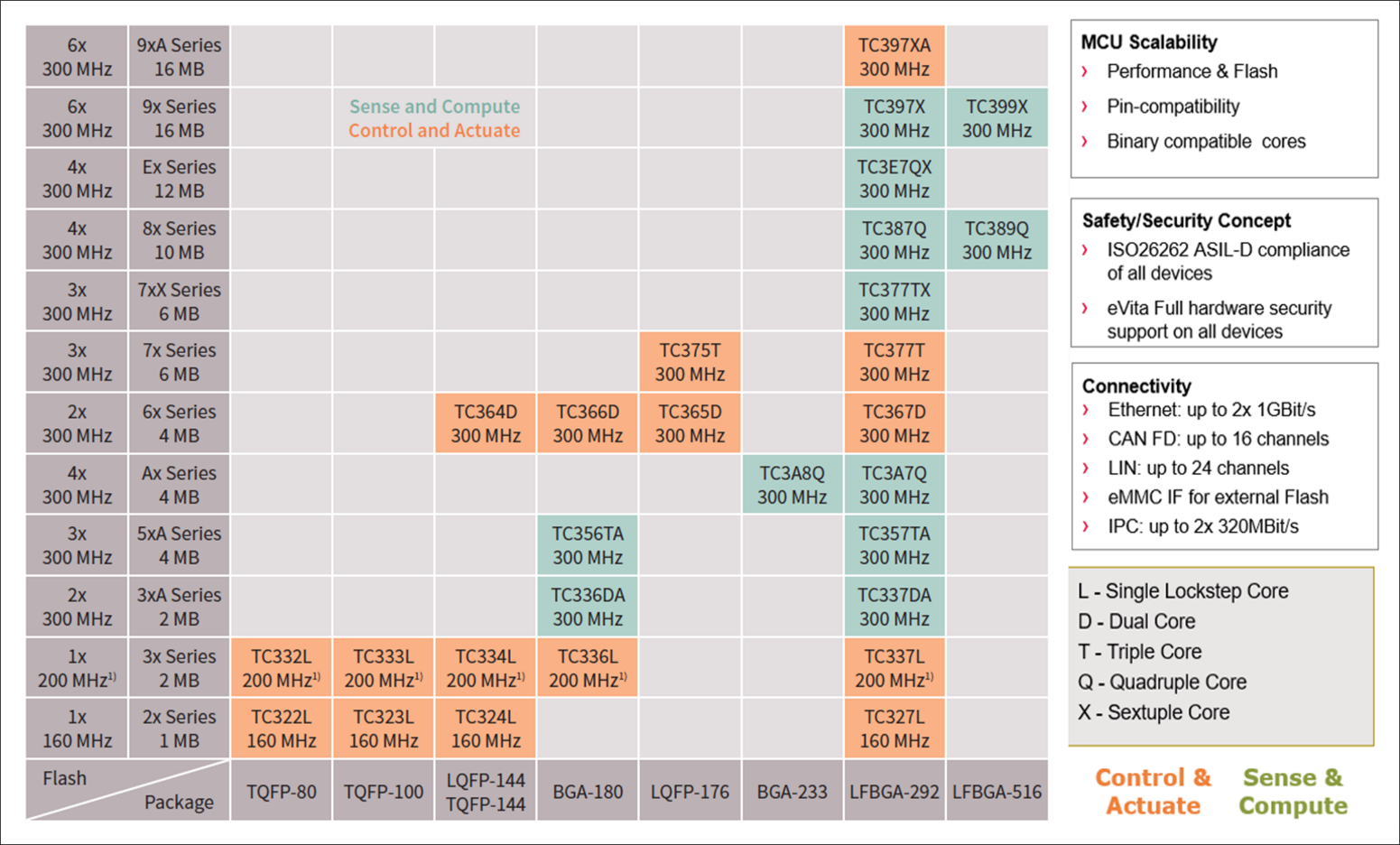
Figure 8. Product selector
Introduction to FUSA application
Application assumptions and implementation of safety functions
Application assumptions are assumptions at the system level, such as safety goals, fault-tolerant time interval and system safe-state determination. Depending on the application fields, a few examples are listed in Section
ISO 26262 - Electric power steering
and subsequent sections to explain how to proceed with the first architecture approach, considering safety-related aspects.
Standards about functional safety aspects
Standards are guidelines and reflect best practices. The functional safety standards differ depending on the sector of applicability. IEC 61508 is widely considered to be the root of all functional safety standards. Following the IEC 61508 standard, many other standards were created for functional safety, for example, ISO 26262 for the automotive sector and IEC 60730-1 Annex H for automatic controls in household and industrial applications.
Figure 9. Functional safety standards overview
Functional safety levels
When planning an ECU, the engineers have more than one safety functionality to implement. Each of the safety elements that are implemented has its own safety classification. In the same MCU, especially if it is multicore, you can set up various independent functionalities; a few of them are not related to safety; others can have a defined safety level.
Depending on the specific application field, the safety levels have the following names:
Automotive standards (ISO 26262): QM, ASIL A, ASIL B, ASIL C, ASIL D
Industrial standards (IEC 61508): SIL 1 and SIL 2, SIL 3, SIL 4
Automatic electronic controls (IEC 60730): Class A, Class B and Class C
The methodology to be applied has a similar basis. Considering the application that is developed and the given technical specifications, a risk analysis needs to be performed to understand which safety goals are to be achieved and their level of criticality with respect to safety (ASIL, SIL and so on), depending on parameters such as severity, exposure and controllability in the automotive field. It is possible to find an example for automotive safety level classification in
Figure 10
.
Figure 10. Establishing the different level of safety in automotive standard ISO 26262
At this point, the project engineers, to whom this book is intended for, can start building their system, considering a good chipset that is adequate to the functionalities they need also from a safety perspective.
AURIX™ TC3xx is designed to be the right MCU for the control board in safety applications, with a significant number of safety mechanisms already built into the hardware. This allows for a fast and reliable system design.
AURIX™ TC3xx MCU and FUSA
shows an overview of the functional blocks available on the AURIX™ TC3xx platform. A clear distinction is made through the colors between cores, memories, peripherals and special features of the product family.
Figure 11. Main features of the AURIX™ TC3xx family
As AURIX™ TC3xx is developed for functional safety use cases, each functional block (apart from a few peripherals) is built to prevent a fault from leading directly to a safety goal violation or to remain latent.
shows a non-exhaustive overview of the hardware safety measures available for each functional block of the AURIX™ TC3xx platform. The main safety features are described in the subsequent subsections.
Figure 12. Overview of the main safety features of MCU blocks
Safety of MCU infrastructure blocks
To execute any safety application software, it is essential to ensure the correct configuration and monitoring of the MCU infrastructure.
By MCU infrastructure, it means:
Common functional blocks: Considered as possible common-cause failure initiators
Access protection features: Provide freedom from interference between HW/SW elements (see Section
Freedom from interference (FFI)
for more information)
Error management and reporting: Provide a transition to the safe state when a fault is detected (see Section
MCU reaction plan - SMU
for more information)
Common functional blocks
Blocks such as the power management system (PMS), clocks, ports, reset and others that are common to all basic functionalities of the MCU are considered always active. They are usually involved in the nominal (also called “mission”) functions and the monitoring functions of AURIX™ TC3xx. Faults in any of these blocks are considered safety-critical and must be detected. In the following sections, an overview of the safety features that are available in these functional blocks is provided.
Power management system (PMS)
The PMS provides the power infrastructure, generates supply voltages using internal voltage regulators, facilitates power distribution and manages system power modes. Monitoring the supply voltages is the main safety activity implemented in the PMS. This consists of detecting overvoltage or undervoltage events at the different supply voltages.
Power built-in self-test (PBIST)
This test is carried out at reset (Cold PORST; see Section
Types of resets
for details on various resets). The goal is to ensure that external power supplies reach a minimal value before reset release. The MCU will remain in a reset state while the defined voltage thresholds are not exceeded
Primary undervoltage monitor
The primary voltage monitor triggers a reset (Cold PORST) if VEXT, VDDP3 or VDD drops below the lowest possible threshold for the correct operation of the system. Reset threshold values are defined in the product datasheet
Secondary overvoltage and undervoltage monitors
The secondary voltage monitor triggers alarms in case of an overvoltage or undervoltage event in any of the supply rails (that is, VEXT, VDDP3, VDD, VEVRSB and VDDM). These thresholds are to be configured by the user
Note:
VEVRSB and VDDM are not monitored by the primary monitor because it is assumed that the secondary monitors are reliable when VEXT, VDDP3 and VDD are within the operating range.
Note:
External supervisors for VEXT overvoltage are supplied at the system level; for example, see Section
Error-correcting code technique
.
Figure 13. Power supply rail internal primary and secondary safety monitors
Clocking system
The clocking system includes the clock generation unit (clock source), clock scaling (PLLs), clock distribution (CCU) and individual clock configurations (for each MCU peripheral). Since the clock signals are distributed to all peripherals, the clocking system is a potential source of common-cause failures. Therefore, fault detection coverage of this block is an important part of the safety measures that are implemented in AURIX™ TC3xx devices.
Hardware measures are implemented to detect faults in all submodules of the clocking system. The main measure is to compare the frequencies derived from an independent clock source against the operating frequency to be protected.
Clock source
The backup clock (internally generated) and the external crystal oscillator (XTAL OSC) are monitored via a watchdog function. An alarm is generated if the number of backup clock cycles within a window of 512 f
PLL0
clock cycles (derived from the XTAL OSC) exceeds a configurable value
Clock scaling (PLLs)
The output of PLLs output is monitored by comparing it against a diverse clock (the backup clock); the backup clock output is monitored by f
PLL0
. A “clock alive” alarm is generated if the monitored clock is below an expected value
Figure 14.
Clock source and clock scaling built-in safety mechanisms
The PLL has a lock detection feature that differentiates between stable and unstable circuit behavior. The PLL may unlock because of a break in the crystal or ceramic resonator or the external clock line. In such a case, a safety management unit (SMU) alarm event is generated.
Clock distribution (CCU)
Clock signals distributed to the individual peripherals must be monitored by the application software. The idea is to compare safety-related peripheral clocks against clocks that are generated from different PLLs, for example:
f
PLL0
(
STM
) vs f
PLL1
(
QSPI
) and/or
f
PLL0
(
STM
) vs f
PLL2
(
ASCLIN
)
Such a plausibility test detects the wrong settings or states of the clock dividers in the CCU logic.
Figure 15.
Clock distribution protected by plausibility check
Clock configuration
In all clocking system subparts, safety-related configuration registers (SFRs) are protected via safety flip-flop (SFF) mechanisms. Safety flip-flops are special flip-flops that implement a hardware mechanism capable of detecting bit flips within the protected registers, thus preventing single-point faults. Alarms will be generated in the event of bit-flip events
System control unit (SCU)
The SCU is a module that includes several central infrastructure submodules, such as the reset control unit, emergency stop, watchdog timers and trap generator (see Section
Interrupts and trap handling
). A set of protection mechanisms (SFFs, signal redundancy and so on) is implemented in the SCU to detect transient or permanent faults that may lead to severe malfunction of the MCU.
The SCU implements the following HW features that are typically required for a safety application:
Watchdog timers
: These timers monitor access to protected SFRs via Endinit or safety Endinit protection (each CPU has a watchdog timer; in addition, a safety watchdog timer is available for shared resources)
Emergency stop (ES)
: The emergency stop feature provides a fast reaction to an alarm without the intervention of the software. As a reaction to the emergency event, selected output ports can be immediately placed into a defined state (for example, bring the actuators into a known state). An emergency stop can be triggered by the following:
A transition on the port that is configured as the emergency stop input
An alarm event or command from the SMU that is configured to generate a port emergency stop
The emergency stop control logic for the ports operates in two modes:
Synchronous mode (default): The emergency case is activated by hardware and released by software
Asynchronous mode: Both the activation and release of the emergency case are done by hardware
Die temperature sensor
To avoid the MCU working outside of the expected temperature range, two temperature sensors are implemented in the AURIX™ TC3xx device. This feature can be used as an additional safety mechanism because it enables the generation of an early warning whenever the die temperature is too close to the boundaries of the operating range. Both sensors are located near areas that are the warmest areas of the product. The first instance (PMS_DTS) is located close to the PMS. The second instance (DTS_Core) is located close to the CPU cluster. Each sensor will detect whether the temperature is within the specified limits and set temperature underflow/overflow alarms accordingly.
Safety of processing blocks
Safe computation - CPU
The TC3xx family utilizes the TC1.62P core hardware, which is based on the TC1.6P core with enhancements in memory distribution, protection and other aspects. Additionally, up to four CPUs are protected by a lockstep mechanism, which allows them to run up to ASIL-D or SIL 3 applications without the need to integrate cyclic software-based self-tests for the CPU.
CPU memory and temporal protection
The CPU offers several HW measures for protection of memory and module resource accesses (registers), as well as timer-based mechanisms for detecting timing violations of the SW.
Lockstep CPU
Depending on the device variant, an AURIX™ TC3xx offers up to four lockstep CPUs. The lockstep (LS) CPU monitoring is based on hardware redundancy with online monitoring of the outputs. The lockstep monitoring function compares the outputs of the master and the checker cores and signals a fault to the SMU for appropriate action.
The monitoring function temporarily separates the cores by inserting delays in the signal chain to avoid an external disturbance that affects both cores in the same way and therefore goes undetected by the lockstep mechanism. To achieve this, the redundant core inputs and the master core outputs fed to the comparators are delayed by two clock cycles, realigning the two signals. The lockstep core has no effect on the nominal operation.
Figure 16. Scheme for an arbitrary node comparator (A) of a lockstep core and its fault injection (B)
The cores equipped with a lockstep also have a continuously running background self-test of the lockstep comparator. The self-test function will inject faults into both inputs of each of the monitored nodes and verify that the fault is correctly detected by the monitoring logic.
shows a simple representation of an arbitrary node comparator and the fault injection mechanism, which is highlighted in green.
All CPU functions are covered by the following lockstep system:
Exception handling
Instruction fetch and execution
Data movements from internal RAM to the core or bus interface
Non-lockstep CPU
The non-lockstep CPU has an identical architecture compared to the lockstep CPU, but it does not include the checker core and the comparator output logic. While the performances of the non-lockstep and lockstep CPUs are the same, the non-lockstep CPU cannot rely on redundant hardware elements. Therefore, a software-based mechanism named software-based self-test (SBST) is required for covering single-point faults and latent faults of the CPU itself.
System timer module (STM)
The system timer is a free-running 64-bit timer that is enabled immediately after an application reset and can be read by the application software. Each CPU has a dedicated STM. The system timer is fundamental for the operating system and task scheduling. It can be configured to generate a compare-match interrupt service routine (ISR) by using dedicated registers. The STM is not part of the duplication area of the CPU, so no specific hardware is dedicated to monitoring the correct behavior of the timer. In cases where the STM is used in safety-relevant applications, the application SW performs plausibility checks using an independent timer.
Error-correcting code technique
Error-correcting code (ECC) is a technique that adds a number of check bits to a message or data, allowing it to detect and correct a limited number of errors. In this scope, the minimum number of bit flips required to change one valid codeword into another valid codeword is called the “hamming distance”. Typical ECCs, such as hamming codes, can detect with certainty up to 2-bit errors and correct 1-bit errors. Hamming codes are used in AURIX™ TC3xx SRAMs. In this case we have single-bit error correction and dual-bit error detection (SECDED). Another type of ECC, such as BCH codes, can be designed to correct multiple-bit errors. BCH codes are used in AURIX™ TC3xx PFlash with dual-bit errors correction and three-bit error detection (DECTED). For DECTED, a hamming distance of six is required.
Figure 17. ECC concept
CPU RAMs
Each CPU utilizes different RAM blocks as local memories, which are represented in
Figure 18
and listed as:
Data Scratch Pad RAM (DSPR)
Program Scratch Pad SRAM (PSPR)
Data Cache (DCache)
Program Cache (PCache)
Distributed Local Memory Unit (DLMU)
Local PFlash Bank (LPB)
Figure 18. Processor core, local memory and connectivity
The processor core connects to these memories and to the following bus interfaces (where these are implemented):
SRI Slave Interface (x2)
SRI Master Interface
SPB Master interface
The CPU RAM can be affected by transient or permanent faults and implements the same safety mechanisms common to all SRAM blocks. See Section
Error-correcting code technique
for more information.
The RAMs of the lockstep CPU are not replicated as part of the lockstep mechanism, but the program memory interface (PMI) and data memory interface (DMI) within the lockstep CPU’s RAM instances , including ECC encoding and decoding, are part of the area of duplication. Lockstep CPU memories are therefore classified as ASIL-D, allowing the user to execute ASIL-D software from a lockstep CPU using any combination of local CPU memory or the memories of another lockstep CPU.
Non-lockstep CPU memories inherit the ASIL-B level from the non-lockstep CPU. If users want to perform ASIL-D read/write operations by using a non-lockstep CPU memory from a lockstep CPU, the system integrator must take care of monitoring data corruption. This means monitoring the data (stored in the CPU.PSPR, CPU.DSPR or CPU.DLMU) of non-lockstep CPUs by using information redundancy.
Nonvolatile memory (NVM)
As shown in
Figure 19
, the MCU features memory resources that are distributed to multiple locations. In particular, the NVM is dedicated to storing data or programs in flash memories. It is composed of the following parts:
Data flash
: Flash banks are used to store application data. Two banks are available (DF0 and DF1)
Program flash
: Flash banks are used to store application SW code or constant data. One bank with local access is available per CPU
User configuration blocks (UCB)
: This block is used for user configuration of the device. It is part of DF0
Flash standard interface (FSI)
: Executes erase, program and verify operations on all flash memories
Configuration sector (CFS)
: This block contains device-specific settings that are not accessible by the user
BootROM (BROM)
: Contains the firmware executed by the device at start-up before user-defined software can be executed
DMU
: Interface the FSI and PFI with data flash, UCB and CFS
Program flash interface (PFI)
: Provides a fast connection between each program flash bank and its CPU
Figure 19. Nonvolatile memory subsystem
Monitoring
The content of PFlash banks is crucial because it contains the code executed by the CPU. Any fault leading to transient or permanent corruption of the PFlash content can lead to severe malfunctions that are not detectable by SW. Therefore, the NVM offers dedicated safety mechanisms for the monitoring of several failures affecting the PFlash. See Section
Error-correcting code technique
for more information.
Each 256-bit block is protected by an enhanced error detection code (EDC) and ECC logic that can detect up to 3-bit errors (TBE) and correct single-bit errors (SBE) as well as double-bit errors (DBE). In addition, a correctable bit address buffer (CBAB) is available to monitor the number and address of corrupted code words; each address is stored only once and an uncorrectable bit address buffer (UBAB) is present to store the address of an uncorrectable error.
To address the latent fault metric of the ECC logic, the PFlash ECC/EDC decoder is also monitored to detect failure modes of the ECC decoder. In addition to all these HW-based safety mechanisms, before starting to fetch safety-relevant code from a PFlash bank or upon every content update, the user application software will execute additional checks, such as a CRC of the full memory.
The nonvolatile memory also has a dedicated RAM for the FSI interface. The RAM can be affected by transient or permanent faults that can corrupt data and it is protected by the same safety mechanisms common to all SRAM blocks.
Volatile memory
In addition to the volatile memories associated with each CPU, AURIX™ TC3xx has EMEM, LMU and peripheral RAMs. A few volatile memories are in a user-accessible memory range. Other memories are localized to the peripheral modules. RAMs are protected, for the most part, by the ECC mechanism. See Section
Error-correcting code technique
for more information. A few exceptions feature EDC only.
Finally, when the ECC detects the majority of the data corruption, the RAM has additional hardware safety mechanisms capable of detecting errors in the RAM address.
The RAM alarm concept is updated based on the expected fault reaction. From each RAM, the following three alarms are sent to the SMU:
Correctable-error alarm (CE): ECC correction is performed (that is, single-bit error correction)
Un-correctable error alarm (UCE): ECC detection (that is, double-bit error) or RAM address error detection
Miscellaneous error alarm (ME): Non-critical (latent) fault detection
EMEM
The EMEM is a dedicated memory that contains RAM blocks (EMEM tiles), which can be used for ADAS applications, calibration or trace data storage. The EMEM implements interfaces to SRI bus and BBB bus.
LMU
The LMU is an SRI-connected module providing access to volatile memory resources. Its primary purpose is to provide up to 256 KB of local memory for general-purpose usage.
SRAM
In this document, the various SRAMs are identified by the name of the functional block where the memory is located. In cases where one functional block has multiple SRAM instances, each memory has a unique identifier.
Functional block | Memory name |
|---|---|
CPU | DSPR |
PSPR | |
DTAG | |
PTAG | |
PCACHE | |
DCACHE | |
DLMU | |
SPU | CONFIG |
BUFFER | |
FFT | |
DMA | RAM |
GTM | RAM |
EMEM | RAM |
LMU | RAM |
PSI5 | RAM |
MCMCAN | RAM |
CIF | RAM |
HSPDM | RAM |
NVM | FSIRAM |
TRACE | RAM |
ERAY | RAM |
AMU | LMU_RAM |
GETH | RAM |
SDMMC | RAM |
SCR | RAM |
MCU function - ADAS
AURIX™ TC3xx supports advanced driver assistance systems (ADAS), a suite of technologies that help drivers stay safe on the road. The main blocks for ADAS are radar interface (RIF) and signal processing unit (SPU).
Radar interface (RIF)
The RIF acts as a 32-bit interface between internal or external ADC channels with the SPU module. The RIF is used in ADAS applications, where a high level of safety is required. Therefore, different parts of the RIF are monitored by HW safety mechanisms. The CRC redundancy technique is used for increasing fault coverage on configuration registers and the data interfaces with the monolithic microwave integrated circuit (MMIC) input stage and SPU output stage.
In the event of an error detection in the MMIC, the application SW performs additional actions to handle errors. Redundancy is applied to the RIF data path and safety mechanisms for increasing data integrity. RIF is a slave node of the FPI and is protected by common access protection safety mechanisms.
Figure 20. RIF overview
Signal processing unit (SPU)
The SPU is a semi-autonomous accelerator for performing Fast Fourier Transforms (FFTs) on data from one or more dedicated ADC interfaces. The SPU uses a three-stage streaming architecture to provide data pre-processing, FFT and data post-processing operations. The SPU uses the radar memory to store datasets and has internal buffer memories, which are used to store the data currently progressing through the processing pipeline.
The SPU is composed mainly of these parts:
SPU core: Computational unit for FFT calculations
SPU lockstep: Full redundancy in case the second SPU is used as a lockstep unit
SPU RAMs: Used for storing data (FFT, BUFFER) and configuration (CONFIG)
Figure 21. SPU architecture
The SPU offers several safety mechanisms that monitor the correct behavior of the unit. During runtime, the SPU configuration data and control flow of the operation are periodically checked. The SPU interfaces with RIF and EMEM are protected by hardware built-in safety mechanisms. The second SPU instance can be configured for full redundancy (comparison of control and data outputs), partial redundancy (comparison of control only) or no redundancy (no comparison).
In the event that SPU is not configured for full redundancy, additional external measures will be implemented at the SW level. A class of faults in the SPU can cause a deadlock in the SPU. A SW-based self-test (SBST) is provided and will detect and signal an error in case the test execution time takes longer than expected. The integrity of a few SPU safety mechanisms is monitored by other dedicated safety mechanisms. SPU is a slave node of the FPI and is protected by common access protection safety mechanisms.
SPU has three different types of RAM, each of which is dedicated to specific usage. Each RAM can be affected by transient or permanent faults that can corrupt data and have the same safety mechanisms common to all SRAM blocks.
Debug and test functionalities
Trace and debug modules are slave nodes of the FPI bus and are therefore protected by common access protection safety mechanisms. Their functionality is disabled during operation. These blocks are protected by hardware safety mechanisms for providing freedom from interference, as described in Section
Freedom from interference (FFI)
.
SRI and FPI busses
SRI bus
The SRI bus connects the CPU, the DMA module and other high-bandwidth requestors to high-bandwidth memories and other resources for instruction fetches and data accesses. The SRI interconnect supports parallel transactions between SRI masters and independent SRI slaves.
FPI bus
The FPI connects the high-speed peripherals (CPU and DMA) to the medium- and low-bandwidth peripherals. The AURIX™ TC3xx family has up to two FPI bus instances:
System peripheral bus (SPB): Main non-ADAS system and communication peripherals
Back bone bus (BBB): Emulation device-related and ADAS-related peripherals, available in ADAS/Emulation
SRI and FPI safety mechanisms
Any R/W operation of the MCU buses can be affected by several faults during the address phase or the data phase, resulting in incorrect or missing data, wrong addressing and so on. SRI and FPI slaves are protected by built-in hardware mechanisms against these possible faults.
MCU function - MCU communication
DMA
The DMA moves data from source modules to destination modules without the intervention of the CPU or other on-chip devices. A data move is defined by DMA configuration data. A DMA channel operation is initiated by a DMA hardware request or a DMA software request.
During DMA operations, transactions can be subject to permanent or transient faults that can affect the success of the data moves in several ways. In addition, the DMA source or destination address can be corrupted, resulting in the wrong data at the destination. Faults in the DMA move engine can lead to lost or delayed transactions. All these kinds of faults are addressed by internal hardware mechanisms.
Interrupts and trap handling
The TriCore™ architecture manual defines how the CPUs deal with interrupts and traps. The interrupt router (IR) module is responsible for scheduling service requests (also called interrupts) to the correct service provider. In the TC3xx architecture, internal peripherals, external hardware or application software can raise a service request. The service providers are all CPU’s and DMA.
The IR is a critical block since a fault in its logic, coming from hardware or software, can affect one or more service providers or the interrupt service routine (ISR). The IR is connected to all internal functional blocks, so a failure in a peripheral can generate malfunctions in the IR and propagate to the CPU, DMA or other peripherals. The correct behavior of the IR and its monitoring functions during runtime are crucial parts of the safety measures implemented in the TC3xx architecture. This is achieved by a combination of internal safety mechanisms built into the hardware and a few software checks.
Trap generation (TRAP) is a functionality of the SCU, which hosts a cluster of sub-modules that control various system functions. SCU trap generation determines which CPU receives a trap based on the trap event trigger. Interrupts can interfere heavily with the sequential execution of the program or be executed as an error reaction, while traps are generated when the core of the MCU detects an error.
Safety of application dependent blocks
Application-dependent blocks are parts of the MCU for which the fulfillment of the safety requirements requires a combination of application-level safety mechanisms and safety mechanisms provided by the MCU. Typical application dependent parts are peripheral modules participating in data-acquisition, actuation control and system-level communication. Correct and safe functionality of the MCU application-dependent blocks can be guaranteed with different techniques.
One of the most common techniques in SEooC peripherals is redundancy with comparison. When redundancy is applied, a dependent failure analysis (DFA) and coverage of common block functionality with additional controls are necessary.
In AURIX™ TC3xx, each identified cause of dependent failures is controlled by an adequate safety measure. One of these measures is the correct pin distribution, as explained in Section
Considerations on common-cause failures on pins and packages
.
Most of the application-dependent blocks use:
GTM modules for generating or capturing signals
ADC modules (EVADC or EDSADC) to perform analog signal acquisition
It is important to briefly introduce the GTM and ADC module concepts before exposing the application-dependent scenarios from a safety perspective.
Overview of GTM
Below is a summary representation of the generic timer module (GTM) that is often used in application-dependent use cases to implement digital acquisition and digital actuation. GTM TIM modules can acquire PWM, while GTM TOM or ATOM modules can generate PWM signals for digital actuation.
The safety mechanism is not in the resource itself (apart from access protection and SRAM ECC), but in the redundancy that is required as an assumption of use, which means implemented by the application engineer.
Figure 22. GTM summary representation
Overview of EVADC/EDSADC
Below is a summary representation of the enhanced analog-to-digital converter (EVADC) block and enhanced delta-sigma analog-to-digital converter (EDSADC) that are often used in application dependent use cases.
The safety mechanism is not in the resource itself (apart access protection) but in the redundancy that is required as an assumption of use.
There are four ADC types present in the MCU:
Delta Sigma: 13 ENOB (effective number of bits), ≤ 200 ksps
Primary SAR: 12-bit, ≤ 2.5 Msps
Secondary SAR: 12-bit, ≤ 1.4 Msps
Fast Compare: 10-bit, ≤ 5 Msps
Figure 23. ADC types
Safe analog acquisition
In AURIX™ TC3xx, the key to achieve the required safety level for analog acquisition is to have a redundant channel called the “monitoring” channel in addition to the functional channel, also known as the “mission” channel. Depending on the safety level required, the input pin for both channels (mission and monitor) will be the same or different. When selecting AD converters for mission and monitoring, the user should ensure to choose ADC blocks guaranteeing physical separation.
shows the case when redundant safety-related analog signals are delivered by the system and redundantly processed by internal resources of the ADC module. The results of the redundant processing are transported from the ADC module to volatile memory and compared by the CPU.
Figure 24. Simplified overview for safe analog acquisition
Note: The system integrator implements a check of the ADC reference voltage, either by an external monitor or by internally converting a known signal and compares the result with the expected value.
Safe digital acquisition
In AURIX™ TC3xx, the key to achieve the required safety level for digital acquisition is to have a redundant channel called the "monitoring" channel in addition to the functional channel, also known as the "mission" channel. Depending on the safety level required, the input pin for both channels (mission and monitor) will be the same or different.
Additionally, regarding the internal peripherals to be used for mission and monitoring, different combinations are possible using independent TIM (timer input) channels of the GTM block or a TIM channel and a "diverse" input timer from an independent peripheral (for example, using CCU6, which is an independent timer module). The CPU reads and compares the results of the signal measurement.
Figure 25. Simplified example of digital acquisition using two independent TIM channels of GTM
For digital acquisition, it is recommended to avoid the use of adjacent pins to prevent common-cause failures of the ports and package (see Section
Considerations on common-cause failures on pins and packages
).
Safe digital actuation
In AURIX™ TC3xx, the key to achieve the required safety level for digital actuation is to have a redundant channel called the “monitoring” channel in addition to the functional channel, also known as the “mission” channel. When selecting internal peripherals to be used for mission and monitoring, different combinations are possible using independent timer output channels and comparing them or reading back. For example, a GTM output timer using a GTM input timer and comparing these two signals.
When a GTM output resource (TOM or ATOM channel) is used to generate the PWM signal, this can be sent back from the external actuator to a GTM input resource (TIM) and application SW can perform a comparison of the PWM output with the PWM feedback signal.
Figure 26. Simplified overview for digital actuation TOM-TIM-SW
For digital actuation, it is recommended to avoid the use of adjacent pins to prevent common-cause failures of the ports and package (see Section
Considerations on common-cause failures on pins and packages
).
Safe E2E communication
Safe end-to-end (E2E) communication is often applied as a safety measure to communication ports instead of using the safety measure “redundancy with comparison”. E2E protocol is a generally well-known safety measure and is also stated in ISO 26262. It is not an Infineon-specific AURIX™ TC3xx safety feature. The AUTOSAR standard also describes a few specifics about this measure.
Figure 27. Types of communications possible with AURIX™ TC3xx
The safety measures are facilitated by using additional meta-data such as CRC, counters and timestamps as part of the payload data. Application software initiates the safe communication safety measures during every communication event (transmission and reception). On detection of a failure, the application SW triggers the reaction. For example, in the case of a transmission error, application SW must re-transmit the same package again. In case of a reception error, application SW will not acknowledge the received package.
The E2E profiles provide a consistent set of data protection mechanisms, designed to protect against the faults considered in the fault model for communication blocks.
Each E2E profile uses a subset of the following data protection mechanisms:
A CRC, provided by the CRC library
A sequence counter is incremented at every transmission request; the value is checked at the receiver side for the correct increment
An alive counter is incremented at every transmission request; the value is checked at the receiver side if it changes, but the correct increment is not checked
A specific ID for every message
Timeout detection: Receiver communication timeout and sender acknowledgement timeout
MCU reaction plan - SMU
The TC3xx is built to be fail-safe, which means the MCU must ensure entering a safe state upon fault detection. To achieve that, the MCU implements a HW infrastructure that is responsible for collecting alarms (fault notification) and triggering appropriate reactions, which is ensured by the SMU. The reaction of each alarm can be configured accordingly to the needs of the application.
The SMU module is connected to all safety mechanisms that are within the MCU to collect alarms. The SMU is also connected to the system control unit, the interrupt router, the ports and the power management system to trigger the configured reaction when an alarm is set.
To mitigate the potential common cause faults, the AURIX™ TC3xx SMU is portioned into two parts:
SMU_core: Located in the core domain
SMU_stdby: Located in the stand-by domain
The SMU_core and SMU_stdby are designed differently and they are located in different clock and power domains with physical isolation between them. The SMU_core collects most alarm signals from the hardware monitors and safety mechanisms according to the safety concept, while the SMU_stdby collects alarms from modules that detect core alive signals, power or temperature failures. This enables the SMU to process any incoming alarm, regardless of the clock frequency used to generate the alarm.
The SMU, in combination with AURIX™ TC3xx embedded safety mechanisms, ensures the detection and reporting of more than 99% of the critical failure modes of the MCU within the fault tolerance time interval.
Figure 28. SMU structure
SMU behavior
Internal failure reporting
The internal failure reporting interface enables the MCU to indicate, via SMU_core, the presence of an internal MCU failure.
The SMU_core can be configured to request one of the following internal reactions to a failure being detected:
Interrupt request for one or multiple CPUs (ISR)
Non-maskable interrupt (NMI)
CPU reset request for one or multiple CPUs
An application or system reset
External failure reporting
The external failure reporting interface enables the communication of the presence of an internal MCU failure to an external safe state controller via SMU_core. Through fault signaling protocol (FSP) pin(s), the alarm information goes to an independent monitor, for example, Infineon technologies OPTIREG™ PMIC TLF35584. This external alarm signal can be delayed by configuring the recovery timer (RT). See
Figure 30
as an example. The SMU can also receive an error notification from an external device via the emergency stop ports and can react to it without the intervention of a CPU.
Alternate external failure reporting
The alternate external failure reporting interface enables the communication of the presence of an MCU common-cause failure to an external safe state controller via an alternative diverse path from SMU_stdby.
On detection of common-cause failure (for example, clock failure, power failure, SMU failure, high or low temperature detection), the SMU_stdby can be configured to set the fault signaling protocol error pin(s) in high impedance state regardless of the port configuration.
Figure 29. SMU internal and external reactions (simplified)
Figure 30. External failure reporting interface - failure reaction example
System level hardware requirements
To cover additional safety aspects at the system level, AURIX™ TC3xx requires the following external safety measures:
Overvoltage monitoring of the two main supplies:
VEXT (V
µC
)
VEVRSB (V
StBy
)
External watchdog
External error signaling to activate an independent secondary safety path
This can be achieved by using, for example, an external power management chip (see
Figure 31
).
Figure 31. TLF35584 connection diagram to AURIX™ TC3xx
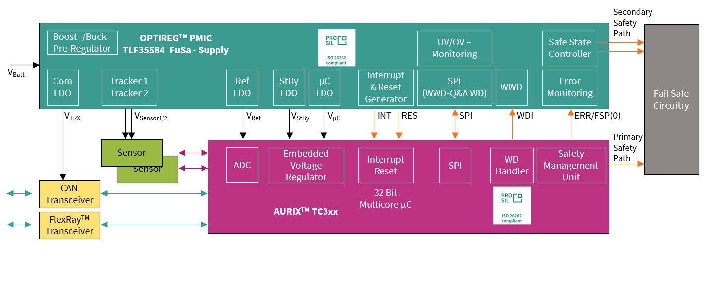
One of the primary roles of this device is to monitor the voltage supplies of the system, whether internally generated by the device or from other on-board regulators and, if necessary, disconnect the MCU from the power supply to avoid a violation of the safety goals.
The Infineon OPTIREG™ PMIC TLF35584 is capable of detecting dependent failures that affect both the function and the diagnostic, such as a watchdog error. When this happens, then the safety power supply can initiate a return to a safe state by driving output pins to disconnect the power feed to the actuators and/or triggering a reset of the MCU.
The safety power supply also monitors the fault signaling protocol (FSP) pin of the MCU that signals an internal failure, indicating that the MCU response is no longer reliable. In this case, the power supply is the ‘last man standing’ and its built-in safe state controller triggers a safe state to meet the safety goals for the system.
As the building blocks of a functional safety system are reviewed and understood, the benefits of sourcing from a single supplier both MCU and PMIC become immediately apparent. Each of the elements of the AURIX™ TC3xx system is specifically designed and tested to work alongside each other and contain signals and controls that significantly ease the task of building a system capable of reaching the highest safety integrity levels.
Safety path
The safety path is the signal chain and circuitry that enables and maintains the system’s safe state. For several applications, the safe state is achieved by disabling actuators, communication channels or the complete system.
In such systems, the safety path is therefore referred to as the safety shutdown path.
Primary safety path
The primary safety path is a safety path (shutdown path) that is managed directly by the safety microcontroller. The microcontroller can keep the application in a safe state if the assumptions of use are respected (for example, operating conditions in a valid range as described in the datasheet) and it is possible to act directly on motor-control signals, communication signals or other possible signals that activate a defined safe state of the system.
Secondary safety path
A secondary safety path is a safety (or safety shutdown) path established through the PMIC’s safety functionality or other external hardware. For example, the safe state of the system in
Figure 32
is intended to be achieved by the PMIC's safe state outputs SS1 and SS2, which should be connected to system circuitry that can release and assert the safe state.
The secondary safety path will be implemented with a high degree of independence from the primary safety path of AURIX™ TC3xx to provide a redundant mechanism for cases in which the primary safety path is unreliable.
Figure 32. Example of primary and secondary safety paths for a communication block
Considerations on common-cause failures on pins and packages
In this section, the topic of common-cause failures (CCFs) in pins and packages will be addressed.
Based on the safety concept for TC3xx, a few functional blocks’ safety mechanisms require the use of two redundant channels (for example, ADC redundant channel acquisition):
Mission channel
Monitoring channel
Figure 33. Channel redundancy representation in the ADC functional block
Common-cause failures are the failure of two or more elements of an item resulting from a single specific event or root cause, which can affect both the mission and the monitor input/output (I/O) signals, potentially leading to failures.
Figure 34. Abstract representation of a common-cause failure
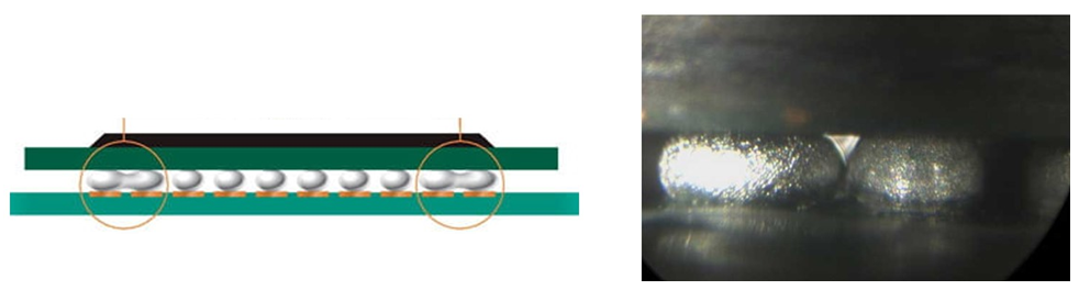
An example of a common-cause failure from the package perspective is when a BGA ball shorts its neighboring balls.
Figure 35. Illustrative example of a common-cause failure from the BGA ball level
shows how a common-cause failure can affect neighboring balls at the package level.
Figure 36. Common-cause failure example
The ball-out of packages LFBGA516 and LFBGA292 is separated into eight different groups. Those highlighted groups indicate that the balls from one group are appropriately separated from the balls from other non-adjacent groups.
The mission I/O pin can be used from one group and the monitor signal can be used from any other group, so that the mission and the monitor groups are not adjacent. This is valid not only for a generic I/O port but also for GTM and ADC modules’ pins when applying the redundancy principles.
As shown in
Figure 37
, if the mission signal is connected to the group highlighted in blue (group 1), then avoid connecting the monitor signal to the same blue group or to the adjacent group marked in yellow (group 2) and the group marked in purple (group 8).
Figure 37. TC399 LFBGA516 I/O configuration
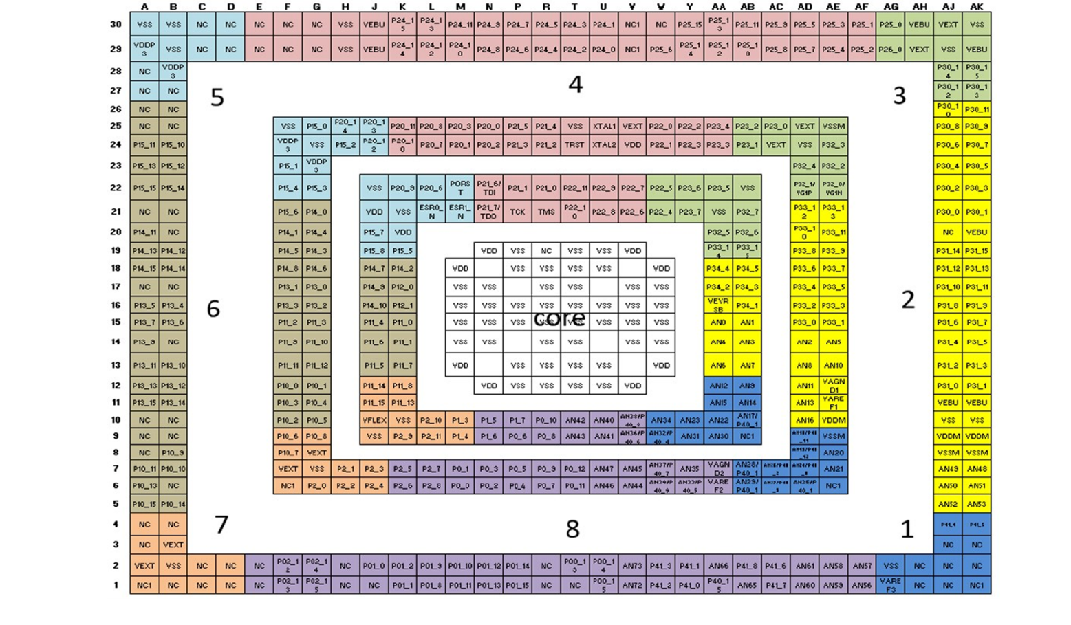
Figure 38. TC3971 LFBGA292 I/O configuration
AURIX™ TC3xx safety package for customers
To enable customers to reach the target safety level for their project, Infineon provides a comprehensive library file that contains all the functional safety documentation related to each specific TC3xx device and is required for the design of a safety-relevant system based on this specific microcontroller. This package is made available to customers under non-disclosure agreement for both ISO 26262 compliance and IEC 61508 compliance justification.
The "safety package" for ISO 26262 is composed of the documents as shown in
Table 3
.
Document | Description |
|---|---|
Safety case report | Serves as the work product requested by ISO 26262:2018 Part 2 Clause 6.5.4 and follows the guidance of ISO 26262, Part 10 Clause 5.3. |
Safety manual | Provides guidance for integrating the device into a safety system, assumptions of use, safety mechanisms and implementation hints. |
FMEDA template | Calculation tool to compute customized ISO 26262 random-fault-related metrics for TC3xx devices depending on the specific configuration for the customer application. |
Safety analysis summary report | Describes the performed safety analysis for the AURIX™ TC3xx devices and provides reference to the corresponding safety analysis results. |
Safety package release note | Present the set of customer-relevant safety documents, taken all together, to enable Infineon to substantiate the functional safety claims. Communicate to the integrator of the AURIX™ TC3xx device the major changes between the documents in this safety package and the documents referenced in the previous package. |
The subsequent sections provide more details about the concept related to metrics such as base failure rate, soft error rate and FMEDA.
Base failure rate (BFR)
The base failure rate (BFR) is the first input of the FMEDA. It is related to the hardware permanent errors only. Data commonly comes from the SN29500 or IEC TR 62380 standards. Infineon’s AURIX™ BFR template according to TR 62380 (or better ISO 26262-11:2018), provides the BFR for permanent faults (hard errors) for the die and the package separately.
The default mission profile is “Motor Control”, as it is the worst-case condition, and working and dormant times for the calculation of τ_i, τ_on + τ_off = 1 were considered. The integrators can change these values based on their own calculations for the mission profiles of the application.
Soft error rate (SER)
The soft error rate (SER) is related to hardware soft (non-permanent) errors and is composed of NSER and ASER data with a package-related adjustment factor, where:
NSER is a soft error rate caused by neutron radiation from cosmic rays at the earth's surface, obtained during accelerated neutron testing. The value depends on the altitude and the location on earth and is referenced to "New York Sea Level". The BFR related to SE caused by neutron radiation (NSER) is multiplied by the value entered in the related cell "Flux Factor for Neutron Particles". For scaling instructions, see JESD89 A.3
ASER is an alpha particle-originating soft error rate obtained during accelerated testing and caused by impurities of process and package materials, for example mainly because of mold compound, and is referenced to low alpha materials. It can also be caused by other materials, such as solder bumps. For bare die applications, the “Flux Factor for Alpha Particles” must be used to scale the SER with an appropriate scaling that considers the alpha activity of the material set for encapsulation and interconnect
As all AURIX™ TC3xx MCUs use low-alpha mold compound (alpha particle emission is 0.0010 cph/cm2) for the packages, the following equation for the SER is applied in the FMEDA.
𝑆𝐸𝑅 = 𝑁𝑆𝐸𝑅 + 𝐴𝑆𝐸𝑅
The soft error rate is independent from the mission profile.
Failure modes, effects and diagnostic analysis (FMEDA)
Failure modes, effects and diagnostic analysis (FMEDA) is the analysis of the effect of random hardware faults on a safety requirement or safety goal, including the quantitative estimation of failure rates and the probability/rate of a safety goal violation.
Infineon provides support for an accurate estimation of the failure rate and diagnostic coverage of the AURIX™ TC3xx MCU, providing a FMEDA template that is fully configurable by the customer for their specific use case for both ISO 26262 and IEC 61508 standards.
Infineon FMEDA supply metrics for:
Permanent faults/hard errors (HE)
: Random HW fault that occurs and stays (for example open, short and so on)
Transient HW faults/soft errors (SE)
: Random HW fault that occurs once and subsequently disappears (for example bit-flip in SRAM because of alpha radiation)
Inputs for the FMEDA Excel sheet come from the BFR calculation and SER.
Figure 39. Infineon FMEDA template, inputs and outputs
ISO 26262 - Electric power steering
To better understand how AURIX™ TC3xx safety features are employed, it is important to discuss a typical application from the automotive sector (an electric power steering (EPS)). A complete chipset, meeting ISO 26262 requirements and supporting fail-safe EPS systems, will be described.
Note: High availability and fail-operational reliability can be achieved by adding a redundant functional system.
The EPS system assists a driver to steer the vehicle with less manual force. The application example of an EPS solution is presented in
Figure 40
.
Figure 40. EPS application example
The electronic control unit (ECU) directly controls an electric brushless direct current (BLDC) motor with 3, 6 or 12 phases, which applies additional torque or force to the steering column or directly to the steering rack. The main hazard is “unwanted steering” which is detected within a fault-tolerant time interval of in the order of milliseconds. The ASIL rating assigned is D.
The critical safety hazard “unwanted steering” comprises faults that lead to unintended generation of torque or moves by the BLDC motor that may lead to steering the vehicle in a hazardous direction. In the event of a detected error, the EPS system will inform the driver with a warning and the driver must be able to control the vehicle manually without interference from the EPS system.
Figure 41. Simplified block diagram of an EPS system
To perform specific tasks, such as steering angle measurement and electric motor control, a number of dedicated integrated circuits are utilized, which are discussed in the subsequent sections. Moreover, their requirements in terms of functionalities and safety-related specifications are described.
Initial assumptions
This example does not cover the steer-by-wire use case; therefore, mechanical steering is considered to be still present. However, the basic requirements for a fail-safe EPS also apply in steer-by-wire systems for each of the redundant functional channels.
Need for protection
EPS uses an electric motor to assist in the steering of a vehicle. A sensor detects the torque exerted on the steering wheel by the driver and an ECU applies assisted torque via the motor. The mechanical linkage between the steering wheel and the steering gear is retained as a backup, so the driver can manually steer the car.
System safe state
: Current flow to the motor is cut off and the motor remains in freewheeling (phase cut-off or active freewheeling). Fail operational may be required, especially for heavy vehicles.
Note: To have a high-availability use case, the example available in this section needs to be reviewed using redundancy.
The EPS system description is represented in
Figure 41
. The main block is the AURIX™ TC3xx microprocessor, which handles and controls all the major functionalities.
Hardware components
The major requirements and the key features of the selected components are:
Safe system supply optimized for EPS with ASIL-D monitoring and supervision
Safe bridge driver, optimal for EPS and brake booster, supporting ASIL-D for safe state off
ISO 26262 compliant angle sensor, torque sensor and motor position sensors designed for most demanding safety applications (ASIL-D) with superior accuracy performance
Robust MOSFET with superior switching behavior
AURIX™ TC3xx- microcontroller that needs to guarantee safe calculation because the output values of the control algorithms heavily influence the generation and control of the BLDC motor. In addition, PWM signals (typically at 20 kHz) for the high side and the low side switches of the half bridge drivers need to be provided safely by the MCU, as well as the SPI for communication with the power supply and watchdog
Current sensors are applied for torque control loops and use multiple redundant ADC channels and converters, for example, dual sensing of 1-3 shunts, using a 4th or using a SPI interface to bridge driver ASICs
CAN (FD) messages for steering angle signal values transmitted outside of the ECU
CAN (FD) and FlexRay (optional) for getting commands in steer-by-wire systems (for example, ADAS commands)
Power supply
The power management IC device can manage and monitor the power supply for a range of ECU component systems, including electric power steering, engine control units and advanced driver assistance systems.
An important functional safety feature of this integrated circuit is its ability to detect and report faults in the power supply rails, such as overvoltage, undervoltage and overcurrent conditions. The device includes a range of built-in protection mechanisms, such as voltage and current clamping, to help to prevent damage to sensitive electronic components in the event of a fault.
The power supply circuit also includes several features to ensure reliable and stable power delivery to critical vehicle systems, including multiple regulated outputs. Each of those can be programmed to a specific voltage and current limit. Another very relevant safety feature is the presence of a watchdog timer to monitor the system for malfunctions and automatically reset the device if necessary.
In addition to its functional safety features, a good power supply integrated circuit is designed to be highly efficient and reliable. The device need to be capable of operating at high temperatures and includes advanced thermal protection features to prevent damage from overheating. An example of such an IC is the TLF35584 presented in
Figure 42
.
Figure 42. Safety connections of the power supply module (besides needed supplies)
Pinout AURIX™ TC3xx-PMIC
lists an example of connections required for functional and safety purposes when using
TLF35584
as the power supply chip for an EPS system. It is necessary to go to the Infineon website to check which is the most appropriate and up-to-date chip variant before making any decision about the project.
NR | AURIX™ | PMIC | Description |
|---|---|---|---|
1 | DATA_IN (RX) | MISO (SDO) | Digital SPI signaling output port refers to the VEXT supply voltage. Connect to the SPI port "data input" of the MCU. |
2 | DATA_OUT (TX) | MOSI (SDI) | Digital SPI signaling input port refers to the VEXT supply voltage. Connect to the SPI port "data output" of the MCU. |
3 | CHIP SELECT | CSN (SCS) | Digital active-low SPI signaling input port refers to the VEXT supply voltage. Connect to the SPI port "chip select" of the MCU. |
4 | CLOCK | CLK_SPI (SCL) | Digital SPI signaling input port refers to the VEXT supply voltage. Connect to the SPI port "clock" of the MCU. |
5 | FSP | ERR | Diagnostic output signal from AURIX™ TC3xx to TLF to activate an independent safety path. |
6 | ESR1 | INT | Safety output to AURIX™ TC3xx |
7 | PORTX.Y | WDI | Watchdog input signal from AURIX™ TC3xx |
8 | PORST | ROT | Reset to AURIX™ TC3xx |
9 | PORTA.B | SS1 | For the startup test of SS1 output effectiveness (optional) |
10 | PORTC.D | SS2 | For the startup test of SS2 output effectiveness (optional) |
3-phase bridge driver
A gate driver IC is dedicated to controlling six external N-channel MOSFETs, forming an inverter for 3-phase motor drives. Such chips are often referred to as gate driver units (GDUs). An example of a block diagram of such an integrated circuit can be seen in
Figure 43
.
Figure 43. Infineon TLE9183QK gate driver connection
From a functional safety perspective, a three-phase driver must include safety features to prevent dangerous situations from occurring in the event of faults.
Some of the key safety features that are typically included in a three-phase gate driver are:
Short-circuit protection of the motor winding
Chip overtemperature protection
Chip under-voltage protection
Overcurrent protection of the motor winding: The internal current amplifier is a circuit that measures the current flowing through the motor windings and amplifies the signal to a level that can be read by the device's control circuitry to ensure safe and reliable operation of the motor
Diagnostic features for chip health management
Pinout AURIX™ TC3xx to the gate driver
shows the connections required for functional and safety purposes when using TLE9183QK as the 3-phase motor driver chip. It is necessary to visit the Infineon website to check which is the most appropriate and up-to-date device before making any decisions about the project.
NR | AURIX™ | Gate driver | Description |
|---|---|---|---|
1 | DATA_IN (RX) | MISO (SDO) | Digital SPI signaling output port refers to the VEXT supply voltage. Connect to the SPI port “data input” of the MCU. |
2 | DATA_OUT (TX) | MOSI (SDI) | Digital SPI signaling input port refers to the VEXT supply voltage. Connect to the SPI port “data output” of the MCU. |
3 | CHIP SELECT | CSN (SCS) | Digital active-low SPI signaling input port refers to the VEXT supply voltage. Connect to the SPI port “chip select” of the MCU. |
4 | CLOCK | CLK_SPI (SCL) | Digital SPI signaling input port refers to the VEXT supply voltage. Connect to the SPI port “clock” of the MCU. |
5 | GTM TOM module | IH1_N | AURIX™ PWM output, TOM channel of the GTM timer |
5 | GTM TOM module | IH2_N | AURIX™ PWM output, TOM channel of the GTM timer 1 |
6 | GTM TOM module | IH3_N | AURIX™ PWM output, TOM channel of the GTM timer 1 |
7 | GTM TOM module | IL1 | AURIX™ PWM output, TOM channel of the GTM timer 1 |
8 | GTM TOM module | IL2 | AURIX™ PWM output, TOM channel of the GTM timer 1 |
9 | GTM TOM module | IL3 | AURIX™ PWM output, TOM channel of the GTM timer 1 |
10 | ADC module | VRO | AURIX™ ADC input; voltage reference output: The DC output voltage at the outputs of the CSAs (VOx) for zero differential input voltage is defined by the output of the reference buffer at pin VRO. |
11 | ADC module Z1 | VO1 | Analog output of current sense amplifier 1 for shunt signal amplification, goes to ADC module Z1 of AURIX™. For functional reasons (synchronization), keep Z1≠Z2; Z2≠Z3; and Z1≠Z3 |
12 | ADC module Z2 | VO2 | Analog output of current sense amplifier 2 for shunt signal amplification, goes to ADC module Z2 of AURIX™. For functional reasons (synchronization), keep Z1≠Z2; Z2≠Z3; and Z1≠Z3 |
13 | ADC module Z3 | VO3 | Analog output of current sense amplifier 3 for shunt signal amplification, goes to ADC module Z3 of AURIX™. For functional reasons (synchronization), keep Z1≠Z2; Z2≠Z3; and Z1≠Z3 |
14 | PORTx.A | ERR_N | Input to the MCU for diagnostic purposes |
15 | PORTy.B | ENA | Enable bridge driver When set to "low", output stages of the gate driver are turned OFF and remain off. Low to high transitions trigger a reset of device-latched errors. |
_ | _ | SOFF_N | Safe Off Not: Switch off paths independent of ENA. Analog active low input pin for external triggering of device safe state. It does not cause the reset of error registers. |
_ | _ | INH_N | Analog active-low inhibit pin. Sets the device into sleep mode for low quiescent current consumption. External FETs are turned off actively before the charge pumps are turned off. Resetting via inhibit requires a new configuration via SPI. |
_ | _ | PFBx | Phase feedback: Not connected to the MCU in this use case |
Note: A PWM clock source plausibility check must be considered.
Sensors and their position
A typical EPS includes a set of sensors to read the motor position, the steering angle and the steering torque, as shown in
Figure 44
.
Figure 44. Sensors position
Torque sensor
The steering torque sensor measures the torque exerted on the steering wheel by the driver. Its signal is fed into the ECU and used to regulate the amount of assisting torque provided by the motor. The torque sensor in this example uses a diverse redundancy such that faults can be detected, for example, using an inverse sensing scheme between the two redundant channels. Torque sensors typically communicate with the AURIX™ TC3xx using the SENT protocol.
An example of a torque sensor is the Infineon hall-based magnetic sensor TLE4999C8, designed for torque sensing applications. One of the key functional safety features is the ability to detect and report faults in the sensor output. This can be achieved through a combination of redundant signal processing and built-in self-test mechanisms.
The redundant signal processing ensures that two independent sensing elements are used to generate differential output signals. These signals can then be compared by the MCU, which does a plausibility check to detect any issue in the measurement chain. The built-in self-test mechanisms allow the sensor to periodically test its own internal components and report any errors or faults to the system control unit.
Figure 45. Dual-die hall-based magnetic sensor characteristic
Another important functional safety feature of the sensor is its ability to withstand harsh environmental conditions, such as high temperatures, humidity and vibration. This can be achieved using specialized packaging and sealing techniques, as well as the integration of built-in protection features such as overvoltage and reverse-polarity protection.
To be easily integrated with other components of the system, such as MCUs and motor drivers, the sensor features a bus-capable digital short-PWM-code (SPC) interface (similar to SENT), which can be easily configured.
Pinout AURIX™ TC3xx to the torque sensor
Figure 46. Infineon TLE4999C8 torque sensor schematic and data example
shows the connection that is needed for functional and safety purposes when using TLE4999C8 as a torque sensor chip. It is necessary to visit the Infineon website to check which is the most appropriate and up-to-date chip before making any decisions about the project.
NR | AURIX™ | Torque sensor | Description |
|---|---|---|---|
1 | SENT | SPC | The two sensor outputs are transmitted using the SPC protocol. |
Figure 47. Sensor communication to AURIX™ TC3xx via SPC protocol
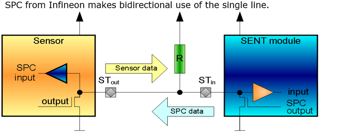
Steering angle sensor (SAS)
The steering angle sensor is typically mounted at the top of the steering column, close to the steering wheel inside the passenger compartment. It is not required for the basic functionality of the EPS system, but it is required for the electronic stability program (ESP), which assists the driver in critical driving conditions. It usually communicates via SENT or SPI to the MCU.
Some of the key safety features for a steering angle sensor in an EPS application are:
Redundancy
: The SAS should have redundant sensor elements and signal processing circuitry to provide reliable operation in case of a single-point failure. This redundancy can ensure that the sensor continues to operate safely and accurately even in the event of a failure in one of the sensor elements
Diagnostic coverage
: Both internal self-diagnostics and external system-level diagnostics (see below explanation)
Accuracy
: The SAS should provide accurate and reliable position sensing to ensure that the EPS system operates safely and predictably
Figure 48. Dual-die angle output of the steering angle sensor
For the above use cases, it uses a dual-die implementation, that is, two fully redundant measurement outputs in one package. In this example, for both chip 1 and chip 2, two different SENT connections are present to transmit the angle sensor measurement; one pin of each chip is the interface for channel 1 and a second pin of each chip is the interface for channel 2. For each single chip, the MCU will take care of a plausibility check to ensure that the two measures are coherent. In addition, another plausibility check is performed to evaluate the information coming from the two different chips and correlate it.
Figure 49. Two outputs from two dual-die-angle sensors
Pinout AURIX™ TC3xx to the steering angle sensor
lists an example of connections needed for functional and safety purposes when using the TLE5014D angle sensor chip with SENT configuration. It is necessary to go to the Infineon website to check which is the most appropriate and up-to-date chip before making any decisions about the project.
NR | AURIX™ | Angle sensor | Description |
|---|---|---|---|
1 | SENT 1 | Chip 1 IFB-1 | Input to MCU - SENT/SPC/PWM/SICI interface for channel 1 First redundant sensor |
2 | SENT 2 | Chip 1 IFB-2 | Input to MCU - SENT/SPC/PWM/SICI interface for channel 2 First redundant sensor |
3 | SENT 3 | Chip 2 IFB-1 | Input to MCU - SENT/SPC/PWM/SICI interface for channel 1 Second redundant sensor |
4 | SENT 4 | Chip 2 IFB-2 | Input to MCU - SENT/SPC/PWM/SICI interface for channel 2 Second redundant sensor |
Figure 50. Sensor communication to AURIX™ TC3xx via SENT
Rotor position sensor
The rotor position sensor is mounted directly at the end of the shaft of the EPS motor, which is commonly a highly efficient BLDC motor. It can use multiple analog signals (sin and cos, resolver) or a digital signal (SENT). There are multiple options for sensing the motor position, for example, magnetic sensors, resolvers and encoders.
Figure 51. Infineon TLE5309A16(D) rotor position sensor wiring diagram
Figure 52. Example of a rotor position sensor with redundancy and diversity
One way to sense motor position is to use a sensor that includes two independent sensing elements, with each element providing a single/differential output signal for both the sine and cosine components of the magnetic field. This results in a total of two/four signals, with one/two sets of redundant signals for each component. The redundant single/differential signals for the sine and cosine components provide several benefits for functional safety.
The bottom sensor element is an anisotropic magnetoresistance (AMR) sensor. Therefore, in the angle range of 180° to 360° of the giant magnetoresistance (GMR) sensor, the AMR sensor output signal will be in the range of 0° to 180° again. This is represented by the blue line in
Figure 52
.
In case a diverse output of the two sensors is desired, the connections to the SIN_N and SIN_P or COS_N and COS_P pins on the printed circuit board can be interchanged. The consequence of this change of connections is that either the differential sine or the cosine signal is inverted, as represented by the dotted blue line in
Figure 52
.
If differential signaling is used (8 connections instead of 4), this can reduce the effects of electromagnetic interference (EMI) on the signal, which can improve the accuracy and reliability of the sensor. This solution also provides a redundancy feature that can help detect and isolate faults in the signal.
Pinout AURIX™ TC3xx to the rotor position sensor
lists an example of connections needed for functional and safety purposes when using TLE5309A16(D) as a rotor position sensor chip. It is necessary to go to the Infineon website to check which is the most appropriate and up-to-date chip before making any decisions about the project.
The TLE5309A16(D) sensor can be used in single-ended or differential output mode.
Figure 52
shows a typical application circuit for the TLE5309A16(D) in single-ended output mode using the positive output channels. For single-ended operation, positive or negative output channels can be used. Unused single-ended output pins should preferably be floating or connected to GND with a high-ohmic resistance (>100k Ω). The TLE5309A16(D) contains separate supply pins for the GMR sensor and the AMR sensor.
NR | AURIX™ | Rotor position sensor | Description |
|---|---|---|---|
1 | DSADCX_a | SIN_P1 | Input to cluster X of DSADC |
2 | DSADCX_b | COS_P1 | Input to cluster X of DSADC |
3 | DSADCY_a | SIN_P2 | Input to cluster Y of DSADC |
4 | DSADCY_b | COS_P2 | Input to cluster Y of DSADC |
5 | EVADCZ1.a | VDIAG1 | Input to cluster Z1 of DSADC |
6 | EVADCZ2.b | VDIAG2 | Input to cluster Z2 of DSADC |
Note: To be able to detect any common-cause failure coming from the MCU, it is recommended that X≠Y and Z1≠Z2. In other words, there must be enough independence between the two redundant ADC acquisitions (P1 and P2) and the same is true for the VDIAGx signal. Separation between sin_P1 and sin_P2, cos_P1 and cos_P2, VDIAG1 and VDIAG2 pins also need to be considered, as explained in Section Considerations on common-cause failures on pins and packages
CAN transceiver
To enable the EPS to interact with the entire car system, an integrated circuit that provides the CAN physical layer is needed. For this reason, a CAN transceiver IC must be selected to enable the AURIX™ TC3xx MCU to communicate using the specific bus protocol.
Some of the key features of a robust CAN transceiver are:
Low current consumption allows the system to accomplish the CAN communication with a small power budget
Fail-safe features such as TxD time-out, RxD recessive clamping (that is, fail-safe feature that prevents sending data on the bus if the RxD line is clamped to high) and overtemperature shut-down allow the system to behave in a predictable manner in safety-critical situations. Other safety measures also report the CAN short circuit proof to ground, battery and VCC, as well as undervoltage detection for the supply voltages
Local failure diagnostics should also be implemented by specifically designed output pins
This IC should be chosen by considering the earlier mentioned characteristics to allow for a safe and reliable communication with the system, as mentioned in Section
Safe E2E communication
.
Figure 53. CAN TLE9252V transceiver pinout
Pinout AURIX™ TC3xx-CAN transceiver
shows the AURIX™ TC3xx-TLE9252V connections.
NR | AURIX™ | CAN | Description |
|---|---|---|---|
1 | _ | CANH | Output of the transceiver to the CAN bus line |
2 | _ | CANL | Output of the transceiver to the CAN bus line |
3 | PORTX1.A1 | NERR | Error flag output, failure and wake-up indication |
4 | PORTX2.A2 | WAKE | Input, sensitive to rising and falling edges |
5 | PORTX3.A3 | NSTB | Standby control input |
6 | _ | INH | Output from external control circuitry—not to be connected to the MCU |
7 | CAN RX | RxD | Receive data output from the MCU |
8 | CAN TX | TxD | Transmit data input from the MCU |
FlexRay communication (optional)
FlexRay is often used instead of CAN in applications where high data transfer rates, deterministic communication and fault tolerance are critical. CAN is a widely used communication protocol in the automotive industry and is suitable for many applications, but it has some limitations that make it less than ideal for safety-critical systems.
One of the key advantages of FlexRay over CAN is its higher data transfer rates. FlexRay supports data transfer rates of up to 10 Mbps, which is significantly faster than the bit rate supported by CAN. This makes FlexRay ideal for applications where large amounts of data need to be transferred quickly and reliably, such as in advanced driver assistance systems (ADAS) and autonomous vehicles.
Another advantage of FlexRay is its deterministic communication. Unlike CAN, which uses a non-deterministic arbitration scheme to resolve conflicts between nodes competing for access to the bus, FlexRay uses a deterministic scheduling scheme that guarantees message transmission times and latencies. This is important for safety-critical systems, where timing is critical and unpredictable latencies can lead to system failures.
FlexRay is also designed to be fault-tolerant, which means that it can continue to operate even if one or more nodes in the network fail. This is important for safety-critical systems, where a single failure can have dangerous consequences.
Some examples of communications in a car that may be implemented using FlexRay instead of CAN include:
Advanced driver assistance systems (ADAS)
: FlexRay can be used to transmit sensor data (for example, radar, lidar, camera) to an ADAS control unit for processing and decision-making
Brake-by-wire systems
: FlexRay can be used to transmit signals from the brake pedal to the brake actuator, providing a more responsive and reliable braking system
Electric power steering (EPS) systems
: FlexRay can be used to transmit steering angle and torque data between the EPS control unit and the steering motor, allowing for precise and accurate steering control
Active suspension systems
: FlexRay can be used to transmit data between suspension sensors and the suspension control unit, allowing for real-time adjustment of the suspension system
CAN is still widely used in many automotive applications and is often the preferred choice for simpler, less demanding communication tasks; however, for safety-critical systems or applications that require higher performance, more robust communication and deterministic timing, FlexRay may be a better option.
Summary
It is important highlighting that it is not possible to add safety features in the last phase of the project development; otherwise, it can be that the MCU does not have enough resources in terms of GPIO and peripherals for redundancy. The correct set of safety features needs to be established at the time the MCU is chosen; otherwise, important safety mechanisms can be missing.
This section underlines that the choice of the correct chipset that is used in a safety application requires a good knowledge of application-related risks, safety goals and safety measures required by each specific functionality.
New trends
For automated driving vehicles or for heavy vehicles, the EPS system must be highly available (ISO 26262: safety-related availability). Typically, two EPS systems are used to achieve fail-safe operational steering. These systems individually apply the same safety methods listed above. The two EPS chipsets either operate in parallel or operate in “hot standby” for the second channel.
In case one channel detects an error, it will stop operation (fail silent). However, in contrast to the standard, there are mechanisms installed that automatically detect a fail silent situation on the other channel, such that the remaining channel can take over the full operation and report the situation to higher-level systems, informing the driver.
Figure 54. Transition from Fail-Safe to Fault-Tolerant EPS
ISO 26262 - XEV traction inverter
The most important system-level blocks of a powertrain system in an electric vehicle (EV) are the electric motor itself, the traction inverter drive, the DC/DC converter, the high-voltage Li-ion battery and the on-board charger (OBC). The traction inverter system is described in detail in the subsequent sections. This system needs to ensure that the vehicle powertrain is operating safely and at optimum efficiency.
Figure 55. Simplified block diagram of the traction inverter system
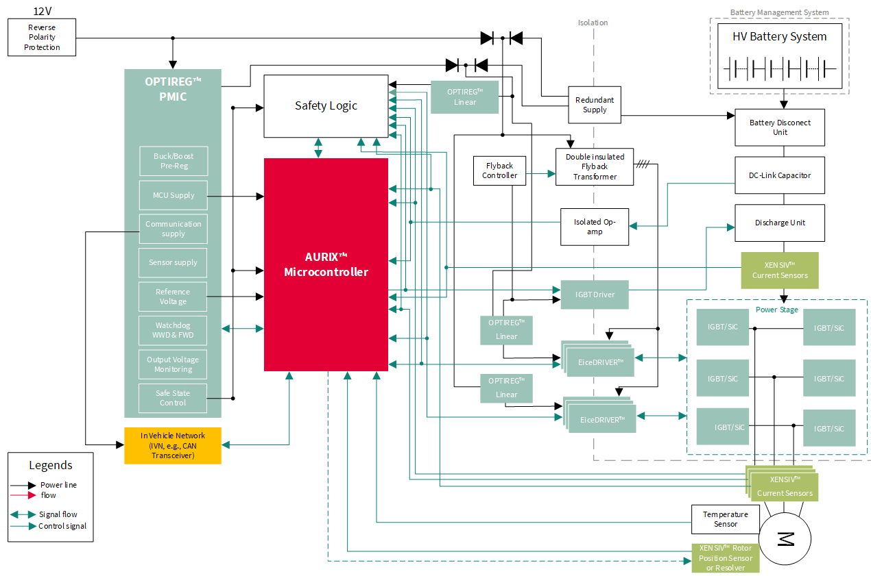
To control the traction inverter, Infineon’s AURIX™ TC3xx MCU family implements advanced features for signal acquisition with the highest safety level (multicore and lockstep architecture, DS-ADC-enabled direct resolver-to-MCU interface, customized PWM pattern generation). Surrounding the 3-phase power stage that will contain Si IGBTs or SiC MOSFETs, there are driver devices that translate the signals from the MCU and provide the necessary isolation.
To provide the multiple rails needed in a traction inverter, Infineon OPTIREG™ power management IC (PMIC) products offer integrated, multi-rail solutions specifically for the harsh automotive environment. Fast 750 V and 1200 V switching devices such as CoolSiC™ MOSFETs are best driven by galvanically isolated gate-driver ICs.
Infineon's EiceDRIVER™ gate driver ICs incorporate the essential features necessary for driving SiC MOSFETs, such as, for example, overcurrent protection, an under- and overvoltage lockout mechanism on all supply lines and support for active short circuit and freewheeling strategies. In addition, the drivers support ASIL-D on the system level, with additional monitoring and supervision functions being integrated to simplify design for safety-relevant applications, including ISO 26262 compliance.
Current sensors in the motor phases and a position sensor on the rotor of the e-motor provide the necessary feedback for precise and energy efficient torque control of the motor, as current sensing is one of the essential measurements within a traction inverter. The Infineon XENSIV™ products offer high-precision miniature coreless magnetic current sensors for AC and DC measurements with an analog interface and fast over-current detection outputs.
Figure 56. Simplified system example of traction inverter
Most state-of-the-art electric vehicles use permanent magnet synchronous machines (PMSM) as the main electric traction motor, typically with three phases. The power range of these motors is from 20 KW up to >100 KW and they normally have 3 or 4 pole pairs with up to ≤25 krpm and a max acceleration of 115.000 rad/s², which requires an output response of ≤ +/-0.2° for 10 krpm. Also, asynchronous e-motors are available, which have less efficiency but the same torque range respect to PMSM. They are anyway bigger and weigh more.
As the manufacturing of permanent magnets requires rare earth material and the recycling process of PMSM often results in the loss of the permanent magnets, the market share of externally excited synchronous machines (EESM) is increasing. These machines generate the magnetic field of the rotor by using copper coils, which are excited by DC current instead of permanent magnets.
Initial assumptions
To build this example, the following initial assumptions are made:
E-motor type: Permanent magnet synchronous machine (PMSM) with rare earth material
Axle propulsion is on the rear wheels of the vehicle
One central traction inverter plus an e-motor for both rear wheels (including a differential and a fixed gear)
Usually, there are two kinds of failures of the motor driver:
Open failure mode
Short circuit failure mode
Phase over-current reaction time, DC-Link overvoltage reaction time and gate driver fault reaction time are supposed to be a few microseconds (to reach a safe state), especially in context with traction inverter components protection
Other hazards that must be considered to maintain vehicle stability on the propelled wheels are considered to have a FTTI of ≤60 ms, for example, "unwanted torque" because of "wrong torque" applied to the wheels without an acceptable tolerance band
The "slow" hazards can be easily controlled by SW, while ultra-fast component protection measures usually require further HW safety countermeasures.
Need for protection
The following are the safety goals when designing a traction inverter:
Avoidance of unintended high voltage (ASIL-B)
This means that the device will not generate induced voltages (acting as a generator) above 60 V without being connected to the HV battery. To fulfill this requirement, the inverter applies, for example, an active short circuit (ASC) on the low- or high-side power switches to actively clamp the motor phases, eliminating the overvoltage situation.
Furthermore, an active DC-link discharge circuit is typically required to decrease the voltage in the DC-link capacitor to below 60 V in a short time (in most applications, it is 2 s). This corresponds to the time, which is considered, for example, for service staff to be able to work safely on a BEV vehicle for maintenance in a garage or in case of a vehicle crash
Avoidance of unintended torque (ASIL-D)
(magnitude, direction and so on): This means that the device will deliver the torque that is requested by the vehicle control unit (VCU) (according to a specific tolerance) with a FTTI of ≤60 ms
Avoidance of overvoltage (ASIL-B)
: During normal operation, the traction inverter control and energy management ECU, between the HV-battery and main inverter, limit the maximum recovered energy that can be accepted by the battery. The traction manager receives the maximum energy limit from the BMS and translates this into a maximum permitted negative torque for the inverter. The inverter controls this by actively setting a negative torque current vector.
The traction inverter is not allowed to provide uncontrolled energy flow into the battery. This is then avoided by an active short circuit at high speed or freewheeling at lower speeds
Hardware components
The major requirements and the key features of the selected components are:
AURIX™ TC3xx MCU family, the traction inverter control core
Power supply for the entire system using a PMIC and other power supply chips such as low-dropout regulators (LDO)
Gate drivers for the six IGBTs or MOSFETs (plus an additional six gate driver boosters, depending on the selected power switches)
IGBT driver for the power transistor for the active discharge unit
Rotor position measurement: To accomplish this task, magnetic xMR angle sensors or a resolver can be used. The acquired data is transmitted to the MCU via CAN (UART). If a resolver is used, the AURIX™ TC3xx family provides support for resolver-to-digital conversion (RDC)
Current measurement for every AC phase of the motor and optionally, also for the DC current from or to the battery
CAN (-FD) Transceiver for communication with the vehicle
Temperature sensors: For example, eMotor-, power module-, PCB- and coolant- temperature
DC-link voltage sensing
AURIX™ TC3xx MCU
To control the traction inverter, Infineon’s AURIX™ TC3xx MCU family offers up to hexa-core performance and advanced features for signal acquisition and pattern generation, connectivity, security and functional safety, ensuring it is ideally suited for many automotive applications, including traction inverter control. Through a closed-loop control scheme, the AURIX™ TC3xx MCU supports the exact torque and speed control of the traction motor. AURIX™ TC3xx can supply many features.
The following are the various timer modules available:
Concatenated advanced timer outputs (ATOMs) + dead time modules (DTMs) for PWM generation, including an adjustable dead time
Dead time module (DTM) shut-off path with TIM input for fast switch-off
CCU6 input for PWM pattern verification
The CCU6 module is not always applied for redundant acquisition or actuation. The choices are multiple and depend on the system integrator’s preference. The same applies for the rotor sensor, which can be plausibly checked by MCU internal rotor position estimators.
Angle and speed feedbacks are often reconstructed by diverse additional observers (for example, Kalman filters) to double-check the function of the primary rotor position sensors. This kind of safety solution allows for ASIL-D supervision for the vital rotor position and speed feedback and inputs for the field-oriented motor control algorithm.
MCU power supply
The power management IC device can manage and monitor the various power supplies of a complex MCU. One important functional safety feature of this integrated circuit should be its ability to detect and report faults in the power supply, such as overvoltage, undervoltage and overcurrent conditions. The device includes a range of built-in protection mechanisms, such as voltage and current clamping, to help preventing damage to sensitive electronic components in the event of a fault.
The power supply circuit should also include several features to help ensure reliable and stable power delivery to critical vehicle systems, including multiple regulated outputs, each of which can be programmed to a specific voltage and current limit. Another relevant safety feature is the presence of a time-window watchdog to monitor the system for malfunctions and automatically reset the device if the MCU is not responding in the right manner.
Additionally, the MCU power supply can request a safe state (independently from the MCU) if it is assumed that the MCU is not working properly. This is a redundant safety path. In addition to its functional safety features, a good power supply integrated circuit is designed to be highly efficient and reliable. The device should be capable of operating at high temperatures (the ambient temperature is often defined in a range between -40°C and 85°C) and include advanced thermal protection features to prevent damage from overheating.
Figure 57. Infineon TLF35584 safety connections of the power supply module (besides needed supplies)
provides an example of connections needed for functional and safety purposes when using the TLF35584 PMIC as a power supply chip. As Infineon is permanently expanding the portfolio with dedicated chips and solutions, check the company website or the regional support for the newest chipset.
Besides the power supply of the AURIX™, the power supply IC also has a supervision function for the microcontroller. During operation, the MCU and the power supply IC are exchanging signal patterns to check if the MCU is still in the right operation and is trustworthy. If the power supply IC is receiving the wrong pattern several times, an MCU power removal can be forced as a safe reaction.
If the MCU cannot be assumed to be trustworthy for executing the right PWM pattern and actions, the power supply IC uses its SS1 and SS2 pins to force the inverter into a safe state (either with active short circuit or freewheeling) without having to rely on the MCU’s functionality. This redundant safety path is a basic need to enable an ASIL-compliant design.
NR | AURIX™ | PMIC | Description |
|---|---|---|---|
1-4 | SPI- pins | SPI- Pins | SPI data transmission for configuration and data readout in a bidirectional way |
5 | FSP | ERR | Diagnostic output signal from AURIX™ TC3xx to TLF to activate an independent safety path |
6 | ESR1 | INT | Safety output from PMIC to AURIX™ |
7 | PORTX.Y | WDI | Watchdog input signal from AURIX™ |
8 | PORST | ROT | Reset to AURIX™ |
9 | PORTA.B | SS1 | For the startup test of SS1 output effectiveness (optional) |
10 | PORTC.D | SS2 | For the startup test of SS2 output effectiveness (optional) |
Gate drivers
Infineon provides an advanced single-channel IGBT driver that can also be used for driving power MOS devices. The device’s aim is to optimize the design of high-performance safety-relevant automotive systems. The gate driver used in this example is based on Infineon’s coreless transformer technology and consists of two chips separated by galvanic isolation. The low-voltage (primary) side can be connected to a standard 5 V logic. The high-voltage (secondary) side is in the HV-battery domain.
Internally, data transfers are ensured by two independent communication channels. One channel is dedicated to transferring the ON and OFF information of the PWM input signal only. This channel is unidirectional (from the primary-low voltage side to the secondary high-voltage side). As this channel is dedicated to PWM information, latency time and PWM distortion are optimized. The second channel is bidirectional and is used for other data transfers (status information, error handling and other functions).
The device supports advanced functions to optimize the switching behavior of the power switches. Furthermore, it supports several monitoring and protection functions, making it suitable for systems that must fulfill ASIL requirements (as per ISO 26262).
The gate driver IC incorporates a serial peripheral interface (SPI) for communication with an external MCU, allowing for bidirectional data exchange and enabling the configuration and control of the gate driver IC. This interface facilitates seamless integration into the overall system and enhances flexibility in driving IGBTs or MOSFETs. In addition, the gate driver IC also features a pulse width modulation (PWM) input. The PWM input enables precise control of the gate driver output signals by accepting pulse width-modulated signals.
Furthermore, the gate driver IC includes fault output pins NFLTA and NFLTB. These pins provide fault status information to the inverter system. When a fault condition, such as overtemperature (of the internal circuitry of the gate driver) or undervoltage lockout, is detected, the NFLTA or NFLTB pins (according to the type of fault) are triggered to indicate the fault condition. This enables the system to promptly respond to fault events, implement appropriate protective measures and ensure functional safety.
As a bridge short circuit (current flowing from HV+ to HV- because the HS- switch and the LS- switch are conducting at the same time) has the highest priority to be avoided, several measures ensure it. At first, the AURIX™ TC3xx is adding sufficient deadtime in between the PWMs for HS and LS to avoid a cross-conduction or shoot-through. If this measure fails, as there is, for example, a single failure on the PCB level, both gate drivers (HS and LS) supervise each other (through INP and INSTP connections) and will not let the opponent gate driver switch on if it is still conducting. Even if this fails, the DESAT detection of the gate driver will recognize the too-high cross-current and turn off the switch. This is an example of how the Infineon chipset ensures a reliable and ASIL-compliant implementation.
Figure 58. Infineon 1EDI2002AS - EiceDRIVER™ and gate driver booster connection schematics
To evaluate the impact of the described functionality on the system in terms of required pins, the Infineon 1EDI2002AS - EiceDRIVER™ is considered as the described IC.
needs to be repeated six times for the six IGBTs or MOSFETs to consider the correct pinout of AURIX™ TC3xx.
NR | AURIX™ | Gate driver | Description |
|---|---|---|---|
1 | GPIO | NFLTA | Fault A output (low-active, open drain). Goes to AURIX™ GPIO as input. This should be combined with the other two EiceDRIVER™ signals on the high side or low side. |
2 | GPIO | NFLTB | Fault B output (low-active, open drain). Goes to AURIX™ GPIO as input. This should be combined with the other two EiceDRIVER™ signals on the high side or low side. |
3 | GTM-(A)TOM | INP | PWM input comes from the GTM timer output module (ATOM or TOM channel). It needs to be connected to the INSTP pin on the other side of the “leg”. |
4 | _ | INSTP | Signal that provides shoot-through protection (STP) to the system. It needs to be connected to the INP pin on the other side of the “leg”. |
5 | GPIO | EN | Enable input. It comes from an AURIX™ GPIO output pin. This should be combined with the other two EiceDRIVER™ signals on the high side or low side. |
6 | VSS | REF0 | The signals INP, INSTP and EN are pseudo-differential in the sense that they are not referenced to the common ground GND1 but to the REF0 signal. This is intended to make the device more robust against ground-bouncing effects. |
7 | GPIO | NRST/RDY | Reset input (low-active, open drain). This signal notifies the AURIX™ GPIO input that the device is “ready”. This should be combined with the other two EiceDRIVER™ signals on the high side or low side. |
8-11 | SPI-pins | SPI-Pins | SPI data transmission for configuration and data readout in a bidirectional way. Daisy chain with the other five SPIs of other EiceDRIVER™. |
When it comes to the combination of six EiceDRIVER™, for both functional safety and hardware protection, it is sufficient, in most cases, to group (OR combination) the faults (faults by NFLTA pin and faults by NFLTB pin) in high-side faults and low-side faults. This results in the following four signals:
High-side fault A
Low-side fault A
High-side fault B
Low-side fault B
Gate driver booster
In high-power applications, such as traction inverters for electric vehicles, the gate driver booster often uses the downstream gate driver to ensure efficient and reliable operation of the power semiconductors, typically insulated gate bipolar transistors (IGBTs) or metal-oxide-semiconductor field-effect transistors (MOSFETs).
A gate driver booster is necessary in the following scenarios:
Faster switching speed
: Power semiconductors in high-power applications often operate at high switching frequencies. The gate driver booster is designed to provide faster rise and fall times for the gate voltage, allowing the power semiconductors to switch on and off quickly. This capability minimizes switching losses and improves overall system efficiency
Driving large gate capacitances
: Power semiconductors, particularly those used in high-power applications, have relatively large gate capacitances. The gate driver booster is designed with sufficient current-driving capability to charge and discharge these capacitors quickly. This ensures efficient switching and minimizes the risk of voltage overshoots or insufficient gate voltage during operation
Improved system robustness
: High-power applications often face challenging operating conditions, such as high temperatures, voltage transients and voltage spikes. The gate driver booster enhances the robustness of the gate driving circuit by providing adequate voltage and current reserves, improving the system's ability to handle such demanding conditions
Compatibility with high-voltage supplies
: In traction inverters and other high-power applications, the power supply voltages can be quite high. The gate driver booster is designed to operate efficiently with these high-voltage supplies, ensuring reliable performance and maintaining the necessary voltage levels for gate driving
Increased redundancy and additional shut-off path
: By adding the booster IC, an important safety feature can be used. As, without the booster, the only shut-off path is just “through” the gate driver, the booster enables direct active short circuit (ASC) functionality, including the possibility of by-passing the gate driver (the ASC pin of the booster)
This integrated circuit is not connected directly to the MCU but instead is cascaded after the gate drivers, so no AURIX™ TC3xx dedicated ports and pins are needed to command this integrated circuit. The integrated circuit taken as a reference for this example is the Infineon 1EBN1001AE - EiceDRIVER™ Boost, which is usually paired with the gate driver described earlier.
When using the ASC functionality, one can benefit from the matched chipset. If the ASC pin is triggered externally, the same signal can be connected to the output stage disable (OSD) pin of the gate driver (see
Figure 58
). The problem is that if an ASC is activated without the gate driver itself enabling it, the gate driver output (TON, TOFF) and the ASC logic can work against each other, which may lead to an unsafe state. Using this connection, the OSD pin of the gate driver sets the gate driver output to “high impedance” and the booster can act as it should without any interference from the gate driver. Normally, the connection is implemented on the low-side boosters.
It is important to explain the need for an external ASC feature. As discussed in Section
MCU power supply
, the MCU supply IC (PMIC TLF35584) is supervising the AURIX™ TC3xx MCU. If any malfunction of the MCU is detected, the supply IC triggers its SS outputs. These outputs can be connected (in combination with additional logic) to this ASC function to enable an ASC on the inverter level, which is not dependent on the functionality of the MCU itself or even on the functionality of the gate driver. This ensures high redundancy and diversity, resulting in a low FIT-rate shut-off path. This feature is not needed in all use cases, but it can be applied when a high ASIL rating is required.
Figure 59. Gate driver and 1EBN1001AE - EiceDRIVER™ booster connections
Rotor position - resolver
Resolvers are absolute-angle transducers that are mounted on the motor shaft to get the motor’s absolute angular position. Resolvers are often used for angle sensing in noisy environments because of their rugged construction and their ability to reject common-mode noise.
Resolver applications, as shown in
Figure 60
, determine the rotation angle by evaluating the induced signals from two orthogonally placed coils, SIN and COS. These coils are excited by the magnetic field of a third coil (EXC). Their amplitudes are modulated with the sine and cosine magnitudes corresponding to the current resolver position.
Figure 60. Resolver system representation
AURIX™ TC3xx family provides support for resolver-to-digital converters (RDC) by providing the following functionalities:
Carrier generation
(EDSADC hardware)
EDSADC hardware supports the generation of resolver excitation carriers by providing PWM pin outputs that can be filtered by a low-pass filter circuit to obtain a pair of differential signals
Signal acquisition and carrier cancellation
(using EDSADC hardware)
Two differential signals are generated from a resolver device (Sin+, Sin-, Cos+, Cos-). These signals can basically be connected directly to the two channels of EDSADC, where each EDSADC channel has P and N inputs
Timestamp acquisition
(using GTM TIM hardware)
Typically, the user's application runs at a different sampling rate than the EDSADC output sampling rate. For example, the motor control PWM interrupt occurs with 10 kHz sampling, whereas the EDSADC interrupt runs with ~9.7 kHz. This condition creates a situation where the sampled resolver position is already aged with a few timer ticks, but this can be significant to the motor control algorithm
Therefore, a timestamp, which indicates the elapsed time since the last EDSADC channel sampling, is required for compensating or computing the missing rotor position. In addition, this timestamp is also used to compensate for the group delay, which is an inherent property of EDSADC.
To implement this functionality into the system, no additional integrated circuits are needed; only the power stages for the S5 and S6 signals and a few other usual passive components are required.
NR | AURIX™ | Resolver | Description |
|---|---|---|---|
1 | DSADC0 | S1 | DS channel x input |
2 | DSADC0 | S2 | DS channel x input |
3 | DSADC1 | S3 | DS channel y input is in a different cluster with respect to S1, S2. It is not necessary to have a different GPIO port, but it is recommended unless you can detect a CCF with a plausibility check. |
4 | DSADC1 | S4 | DS channel y input |
5 | DSADC2 | S5 | Carrier generation |
6 | DSADC2 | S6 | Carrier generation |
In this example, redundant measurements could be considered. Using system properties to do a plausibility check on the sine and cosine values requires a good knowledge of the system. In the scope of this document, it can be simpler to duplicate channels using enhanced delta sigma ADC (DSADC) or enhanced ADC (EVADCs) for the sensor feedback. Furthermore, the excitation signal (also known as the carrier generator signal), which delivers a known data sequence, should be read back with an EVADC or EDSADC channel by the MCU.
In addition, there are other common-cause failures in ADC modules; for example, the analog voltage reference (VREF) requires a dedicated safety check that allows to deduce unintended drift of the analog signal conversion. Here, multiple solutions are feasible, such as using a redundant second VREF, which can be compared to the main one or the internal bandgaps of the MCU itself.
It is important to make the following general considerations about resolvers:
As a Safety Element out of Context (SEooC), AURIX™ TC3xx safety concept will require DSADC redundancy for each analog acquisition
In the context of resolver measurement, the physical properties of the coils’ relationship are well known; consequently, plausibility checks between signals are possible and can be used for safety purposes. Examples of signal properties well known are:
Zero crossing twice per period with a 90° phase shift
sin
2
- cos
2
= 1
Relationships between signals as listed above can be very strong to fulfill ASIL rating requirements when accompanied by timestamp acquisition and a robust plausibility check. The decision of which is the best solution for the specific resolver should be taken by the system engineer who is in charge of all the system aspects.
Current measurement
The current sensor from Infineon is a highly reliable and functionally safe solution designed for accurate current measurement. It offers a range of features to ensure safety and precise operation.
Figure 61. Current sensing example: Lateral sensor insertion
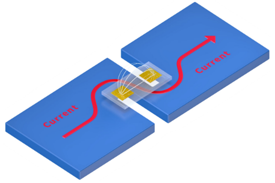
The sensor is equipped with two independent fast over-current detection (OCD) pins, enabling efficient monitoring and protection against excessive current levels. These pins provide an additional layer of safety by allowing the system to quickly respond and mitigate potential risks associated with overcurrent conditions, which are programmable by the customer for specific thresholds and deglitch timings. The OCD pins are designed as open-drain outputs and can be connected to the logic input pins of the MCU and/or the pre-driver to quickly react to over-current events. The OCD1 pins can be easily setup in a wired-OR configuration to monitor several current sensor outputs via only one MCU pin.
The advantage of the additional OCD2 pin is the low latency in the detection of positive and negative overcurrents. Depending on the primary current slope and the programmed threshold, detection latencies of about 1 us can be implemented with the Infineon current sensor. This enables fast hardware protection. OCD2 pins from different sensors should not be connected together if diagnosis mode is enabled (default). In this case, the OCD2 fault indication of one sensor may unintentionally activate the diagnosis mode on the other sensors by forcing the pin to ground.
Another notable feature is the configurable analog output operational mode. It offers flexibility in selecting the operational mode, whether fully differential or single-ended. This adaptability enables seamless integration into different system architectures, catering to specific application requirements and optimizing overall performance.
Figure 62. Application circuit for TLE4972 current sensor, fully differential and single-ended
The current sensor combines precise current measurement, independent overcurrent detection pins, configurable operational modes and a robust design compliant to functional safety rating (ISO 26262 ASIL B).
To evaluate the pin requirements of the system implementing the current sensing functionality, the Infineon TLE4972 is considered a reference.
shows connections with three current sensors, included in the pin count for differential mode connection.
NR | AURIX™ | Current Sensor | Description |
|---|---|---|---|
1 | DSADC0 | VREF Sensor x | Reference voltage I/O, analog output signal in fully differential mode, synchronized with ATOMs PWM pattern to the gate driver input to AURIX™ TC3xx delta sigma ADC module |
2 | DSADC0 | AOUT Sensor x | Analog output signal (for TLE4972): Input to AURIX™ TC3xx delta sigma ADC module |
3 | GPIO | OCD1 Sensor x-y-z | Over-current detection output 1 (open drain output) Wired OR of all OCD1 pins of the three current sensors |
4 | GPIO | OCD2 Sensor x | Over-current detection output 2 (open drain output) of current sensor x |
5 | DSADC1 | VREF Sensor y | Reference voltage I/O, analog output signal in fully differential mode, synchronized with ATOMs PWM pattern to the gate driver input to AURIX™ TC3xx delta sigma ADC module |
6 | DSADC1 | AOUT Sensor y | Analog output signal (for TLE4972): Input to AURIX™ TC3xx delta sigma ADC module |
7 | GPIO | OCD2 Sensor y | Over-current detection output 2 (open drain output) of current sensor y |
8 | DSADC2 | VREF Sensor z | Reference voltage I/O, analog output signal in fully differential mode, synchronized with ATOMs PWM pattern to the gate driver input to AURIX™ TC3xx delta sigma ADC module |
9 | DSADC2 | AOUT Sensor z | Analog output signal (for TLE4972): Input to AURIX™ TC3xx delta sigma ADC module |
10 | GPIO | OCD2 Sensor z | Over-current detection output 2 (open drain output) of current sensor z |
In addition, the current sensor depicted on top of the power stage in
Figure 55
is optional and usually found in most complex inverters. The control of the inverter is fully doable without the mentioned current sensor, but it gives additional information that may be used for plausibility checks, for example, power comparisons between the AC and DC sides. The power at the DC side can also be calculated using the voltage measured at the DC-link capacitor.
It is important to make the following general considerations about current measurements:
As a Safety Element out of Context (SEooC), the AURIX™ TC3xx safety concept will require ADC redundancy for analog acquisition
In a 3-phase current measurement context, the physical properties of the current signals are well-known; consequently, plausibility checks on AURIX™ TC3xx between signals are possible. Examples of signal properties well known are:
Zero crossing twice per period with a 120° phase shift
IA + IB + IC = 0
The PWM pattern is well known, so it is possible to know which currents are physically possible
The above-listed plausibility checks are useful to develop a good safety solution.
Other common-cause failures in ADC modules should be considered; for example, the analog voltage reference (VREF) requires a dedicated safety check that allows for the detection of unintended drift. Here, multiple solutions are feasible, such as using a redundant second VREF, which can be compared to the main one or the internal bandgaps of the MCU itself.
As the current sensors are individual sensors, they can also be supplied with different supply voltages to ensure a redundancy in supply if requested by the safety requirements. Further things to be checked from a safety perspective include, for example, broken wire detection. An indication of typical failure modes to be considered in an analog acquisition can be found in the MCU safety manual provided under the non-disclosure agreement (NDA).
Temperature sensor
The temperature sensor is often implemented as an analog device specifically designed for accurately measuring the temperature of a board component or system part, enabling further safety monitoring and control. This is not a mandatory safety measure but is commonly used to check that the working temperature range of the system is not exceeded.
One important factor is accuracy, which should be maintained across a wide temperature range, allowing for effective monitoring in both extreme hot and cold conditions. The sensor's output represents the temperature being sensed, enabling easy interpretation and integration with existing systems.
To perform out-of-range detection within the AURIX™ TC3xx, the temperature sensor, its supply and the circuitry around it must be designed to ensure normal operation between 0.5 V and 4.5 V at the ADC pin of the AURIX™ TC3xx. This enables monitoring to determine if the signal is within this range or outside. If it is outside the range, a wire may be broken or the supply may be missing. This is important to verify the plausibility of the measured temperature value. As for the purpose of this example the temperature is a “complementary” measure; it is therefore not considered redundant.
NR | AURIX™ | Temperature sensor | Description |
|---|---|---|---|
1 | VADC | Vout | Voltage output for temperature value |
Note: AURIX™ TC3xx also offers die temperature sensors (DTS), which can be used from a safety concept perspective as a complementary source of input to perform plausibility checks (see Section Die temperature sensor).
CAN transceiver
To make the inverter integrated within the entire car system, an integrated circuit that accomplishes CAN communication is needed. For this reason, a CAN transceiver must be selected to enable the AURIX™ TC3xx MCU to communicate using that specific bus protocol.
Some of the key features of a good CAN module are:
Fail-safe features such as TxD time-out, RxD recessive clamping and overtemperature shut-down, that allow the system to perform in a predictable manner in a safety-critical situation. Other safety measures also report the CAN short circuit proof to ground, battery and VCC, as well as undervoltage detection on the supply voltages
Local failure diagnostics should also be implemented by specifically designed output pins
Keeping into account the earlier mentioned characteristics of a CAN transceiver, the Infineon TLE9252V CAN transceiver is taken as a reference to understand how the CAN functionality can be integrated into the safe system itself.
Figure 63. TLE9252V CAN transceiver connections with MCU and power supply
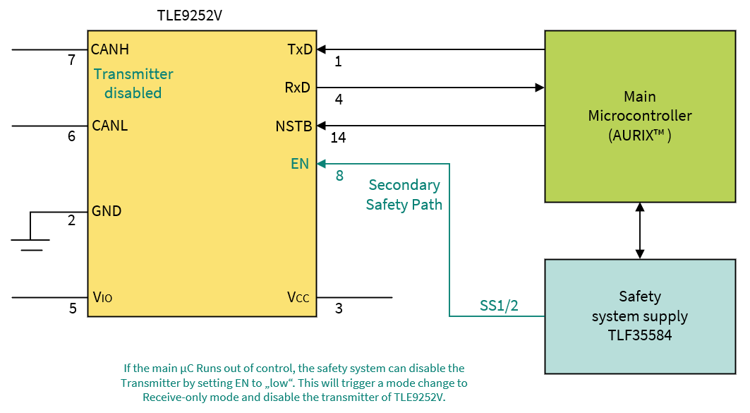
Referring to
Figure 63
, the connection required with the MCU is reported in
Table 15
.
NR | AURIX™ | CAN TR. | Description |
|---|---|---|---|
1 | CAN | TxD | Transmit data input from the MCU |
2 | CAN | RxD | Receive data output to the MCU |
3 | GPIO | NSTB | Stand-by control input (for the transceiver) |
IGBT driver for active discharge unit
In an active-discharge-unit application for inverters, the IGBT plays a critical role in managing the discharge process effectively and safely. It is specifically designed to handle the controlled and gradual release of energy from the inverter's capacitors or energy storage devices.
One of the notable features of this IC is its capability to provide a fast discharge path. It facilitates rapid and efficient energy release from the capacitors, aiding in reducing the residual voltage within a short span of time (in most cases, 2 s).
To ensure the safe operation of the system, the IC incorporates various protection mechanisms. It includes features such as overcurrent protection, overvoltage protection and thermal protection. These safeguards prevent any potential damage or overheating during the discharge process, thereby enhancing the safety and reliability of the inverter system.
The IC also offers a control interface that enables seamless integration with the overall inverter control system. It allows external control signals to initiate or halt the discharge process, facilitating coordinated operation and control over the energy discharge.
Figure 64. Infineon AUIRS212 IGBT driver connection scheme
In summary, the IC used in the active discharge unit application for inverters, enables safe and controlled discharge of energy from the inverter's capacitors or energy storage devices. The reference taken for this use case is the Infineon AUIRS212.
NR | AURIX™ | IGBT driver | Description |
|---|---|---|---|
1 | GPIO | IN | Logic input for gate driver from the MCU |
2 | GPIO | FAULT | Indicates an over-current shutdown has occurred, signal going to the MCU |
DC-link voltage sensing
In a traction inverter, the DC-link voltage can be sensed using a delta-sigma modulator and a digital isolator.
A voltage divider reduces the actual DC-Link voltage to an analog signal (-1 V to 1 V), which is then converted into a bitstream. The clock (for example, 10 MHz) to synchronize the delta-sigma modulator and the MCU can be sent out by the AURIX™ TC3xx itself to avoid another clock generator. This digitalized voltage is processed within the control system for closed-loop control, fault detection and protection purposes, providing accurate sensing with electrical isolation.
Figure 65. Voltage sensing connection
As per
Table 17
, three pins are required for the MCU in the system.
NR | AURIX™ | DC-link voltage | Description |
|---|---|---|---|
1 | GPIO | STAT | indicator output from external chip to MCU |
2 | EDSADC clock | CLK | Modulator clock output from EDSADC of MCU to the external modulator |
3 | EDSADC | OUT | External modulator data output from external chip to the MCU EDSADC |
Power management and redundant supply
The power supply concept of a main inverter with redundant supply from a 12 V chassis battery and from an HV battery is mandatory to maintain under all circumstances the safe state of a traction inverter. There are basically two main supply sources, handled by a fly-back controller and a transformer.
In this system, the “continuous supply” concept is implemented, which means that it does not matter whether the supply comes from the high voltage or not. Basically, if one supply fails, the redundant one will still allow the system to run and the safety logic to handle the situation as intended.
When two diodes are placed in opposite directions, as shown in
Figure 66
, it is possible to find a redundancy node where there is an “OR” between the low voltage supply and the high voltage supply, coming from the redundant supply. What is between the two diodes (the power supply branches going to the flyback transformer and to IGBT’s) go into the flyback transformer to ensure galvanic isolation and a different number of windings for the secondary side to get a higher voltage level for the secondary side of the gate drivers with respect to the primary side. On the secondary side, there will be at least four lines, of which three are dedicated to the high-side gate drivers for the H-bridge and one for all low sides.
Figure 66. Redundant supply representation
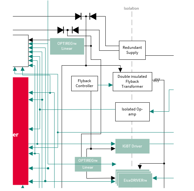
The reason why the system needs a separate voltage for each high-side gate driver is that the imposed voltage into the gate is related to a floating voltage reference (phase voltage); instead, on the low side, the reference voltage is the minus pole or negative terminal of the battery. Power lines in some systems can be six, one for each gate driver, especially for fast-switching SiC applications. There are many other possibilities to implement a redundant supply; the one depicted here is reported as an example.
Safety considerations - inverter safety logic
For the inverter use case, cars can have either front wheel drive or rear-wheel drive. This can cause some serious issues since applying the wrong torque to the rear side of a car makes the vehicle’s dynamics change dramatically and it is easy to lose control of the vehicle. The car makers focus on what happens when the motor is failing and on controlling how it fails, since the severity of the fault is high. The safety logic unit is not inside the MCU but is physically separated. This block is a redundant logic on the system level that supervises signals and can react independently. In a few inverter applications, the safety logic will be a complex programmable logic device (CPLD) or a field programmable gate array (FPGA); in other applications, it can be a second MCU that handles small tasks such as phase overcurrent monitoring, overvoltage and safe state switching. Note that a second MCU also must maintain, under all circumstances, the permissible FTTI safety limits; therefore, software tasks may face the same limitations as on the main MCU.
For inverter applications, the inverter cannot detach itself from the wheels as it can be for an EPS system, but the battery can. For example, in the case of braking using the electric motor for energy recuperation, the inverter will inject a lot of energy into the high-voltage (HV) grid of the system if the HV battery is not fully loaded yet. See
Figure 67
to understand the entire power flow diagram, including the recuperation phase.
Figure 67. Power flow diagram for a two eAxle electric vehicle (EV)
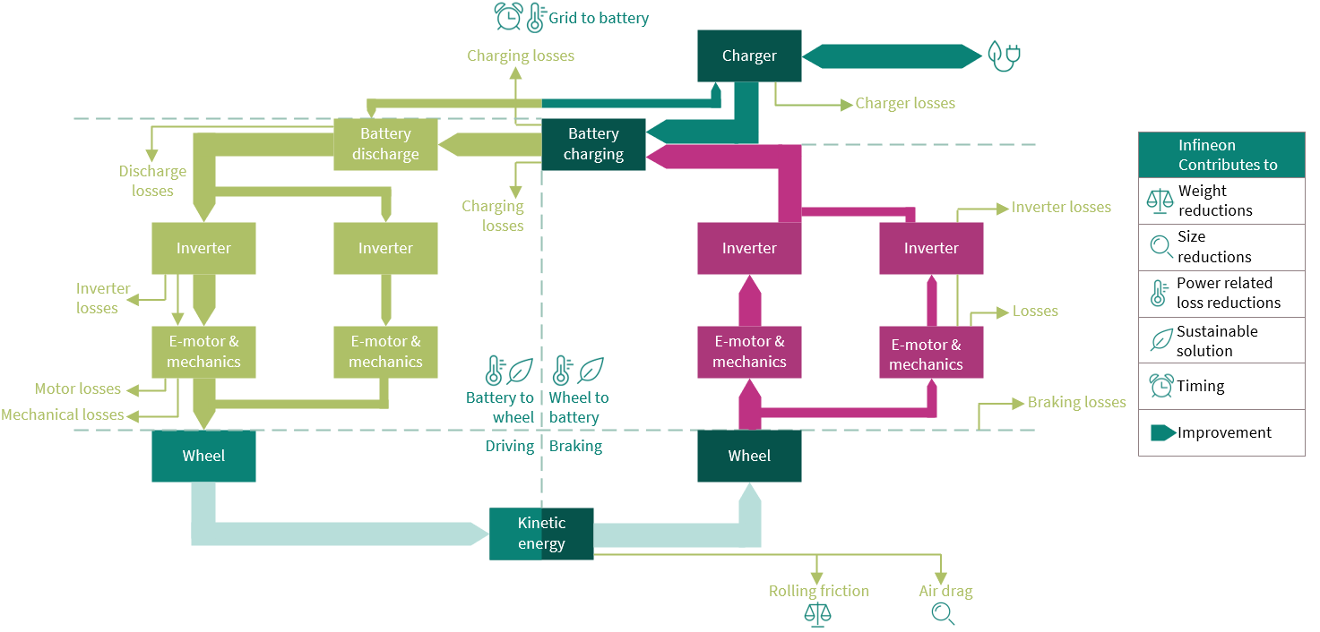
In case the battery is disconnected during the recuperation phase (deceleration), this can cause some serious damage to the circuits as the inverter cannot “push” the current to the battery. Therefore, the inverter must react within hundreds of microseconds to avoid destructive overvoltage. This happens, especially if the motor goes into the “field weakening” mode, because the motor can feedback to the inverter voltages that are higher than the maximum withstand voltage (>1200 V) of the components inside the inverter.
For this reason, the “safety logic” integrated circuit must make sure that the inverter triggers an ASC to the traction motor, clamping the voltage to zero either on only the high side or alternatively on only the low-side IGBT drivers, to not generate back electromotive force (EMF) when the electric motor is turning. Nevertheless, in dependence of the traction motor type (for example, PMSM), this state may not be allowed in certain lower rpm ranges (for example, below rated PMSM motor speed), as here the generated negative brake torque may lead to locking the propulsion wheel(s) and by this risking vehicle safety again. For this situation, free-wheeling (all switches open) may be the better choice, as long as the generated voltage to the IGBTs does not exceed the maximum electrical IGBT break-through voltage.
As can be easily seen from the example discussed in this section, a safe state of a traction inverter may consist of not only one single reaction of the system but also of a combination of multiple states depending on the application environment.
Trends
Further integration trends, such as combining an on-board charger (OBC) with the inverter and reusing the motor stator windings of the PMSM for grid charging, will add additional requirements to the MCU, such as isolation supervision versus grid and enlarged operating hours because of the added time for charging.
Autonomous driving vehicles can require redundant inverter electronics and 6-phase e-motors (2x3 phases). This does not change the ASIL-related requirements for the single-inverter electronics themselves.
Safety software enablement and AURIX™ TC3xx
The AURIX™ TC3xx features enable customers to develop application software up to the most stringent safety standards, effectively meeting all specified requirements. Functional safety software will mainly guarantee two aspects:
The safety of the SEooC itself
The safety of the function that is intended to be implemented with the help of the MCU
This means that parts of the safety code will be necessary to complete the safety tests of the internal blocks of the MCU (for example, fault injections, clock plausibility, ADC voltage reference test and so on) and parts of the safety code will be in charge of implementing the application-specific safety functions.
All this safety code needs to be inserted into a well-structured architecture. When starting with the task of designing the software architecture, the initial set of inquiries that need answers may include:
How to perform initialization (which MCU core should start, what to do later, when enabling interrupts and what to do when coming from standby)
How to react to a fault (types of possible reactions and, in the case of a reset reaction, what kind of reset and so on)
How to use multicore architecture in the best way
How to organize safety and non-safety code partitioning (data protection, program protection, temporal protection) considering freedom from interference aspects
In the following sections, these points will be analyzed deeply, allowing the reader to understand how the AURIX™ MCU can fulfil the earlier mentioned topics.
MCU operating modes
One of the features of the MCU is its ability to operate in different modes, which allows it to adapt to various requirements and efficiently manage power consumption. These operating modes enable MCUs to balance performance with energy efficiency, making them suitable for a wide range of applications. By utilizing different modes, developers can optimize the behavior of an MCU, ensuring it meets the specific needs of their embedded systems without removing power when not necessary, and enhancing the overall performance.
At any point in time, the MCU will be in one of the following modes:
Completely unpowered
The MCU is not supplied and no energy is provided to the device. No internal circuitry is active
Reset mode
While in this state, the I/O pins are in a reset state and the internal modules are kept in a known state and are inactive
Power-up mode
When the voltage supplies reach a certain threshold, the internal circuitry is activated and all modules and memories are initialized. If initial tests are successful, CPU0 is released from reset and the startup software is executed. During this phase, the safety mechanisms are initialized and tested by the startup software
Run mode
If all tests are successful, the CPU0 releases the other CPU and the application software is executed. All necessary safety mechanisms are supposed to be active, even those that require software configuration. This is the normal state of the MCU during operation
Internal error mode
Because of an internal failure, the MCU outputs are potentially dangerous. The user can configure the dedicated FSP error pin to signal this state so that the "secondary safety path" can be activated
Standby mode
This mode is entered on a SW request or because of an ESR1 assertion event. In this mode, only the standby controller and the wake-up unit are active. All other peripherals and CPUs are switched off. Ports are set to their default state. No safety mechanisms are active
Sleep mode
This mode is entered by SW request. CPU code execution is halted and CPUs are held in an idle state. Peripherals are in a sleep state and ports keep their programmed value. No safety mechanisms are active in the "sleeping" blocks
Debug mode
This mode is enabled to allow the developer to access HW registers and functions during the development phase. In debug mode, the safety mechanisms are active, but there is no guarantee that the debug module (OCDS) in the device will not interfere with the HW. Therefore, no safety-relevant applications should run in this mode
The only mode assumed in the safety concept of the MCU is run mode.
Types of resets
AURIX™ TC3xx has a scalable reset concept, where different types of resets are encapsulated one into the other. The cold power-on reset is the highest reset type, where the embedded voltage regulator (EVR), internal clocks and RAMs are reset in addition to the modules affected by the application reset, system reset and warm power-on reset. In addition to the resets affecting all the modules, there are also SW module reset and debug reset that enable the user to directly trigger a reset of the connected modules.
Depending on the number of modules involved in the reset, the following are the different kinds of resets:
Cold Power-On Reset
A Cold Power-On Reset is a reset that is triggered for the first time during a system power-up or in response to a temporary power failure. The pins and internal states are placed immediately into their default state when the trigger is asserted. The system is placed in a defined state and all registers keep their reset values as long as the reset is asserted. Data scratch pad RAM (DSPR), program scratch pad RAM (PSPR) and local bus memory unit (LMU) are re-initialized only after a cold power-on reset. In all other reset types, their content and redundancy are not affected
Warm Power-On Reset
A warm reset is triggered while the system is already operational and the supplies remain stable. It is used to return the system to a known state. On a warm reset request, port pins are immediately placed in the default state and all internal peripherals and the CPU are re-initialized.PORST pin assertion keeps the MCU in warm power-on reset type
System Reset
As for the Warm Power-on Reset, this reset leads to an initialization into a defined state of the complete system. This type of reset can be triggered intentionally by the application software by configuring specific registers
Application Reset
This reset leads to an initialization into a defined state of the complete application system, which means all peripherals, all CPUs, all pins and part of the SCU. As for system reset, application software can configure the trigger sources
Module Reset
Individual reset commands can be sent by authorized masters to a single module without any impact on the rest of the system
shows the different kinds of resets and their effects on the various parts of the MCU.
Figure 68. Different kinds of resets and their effects on the various parts of the MCU
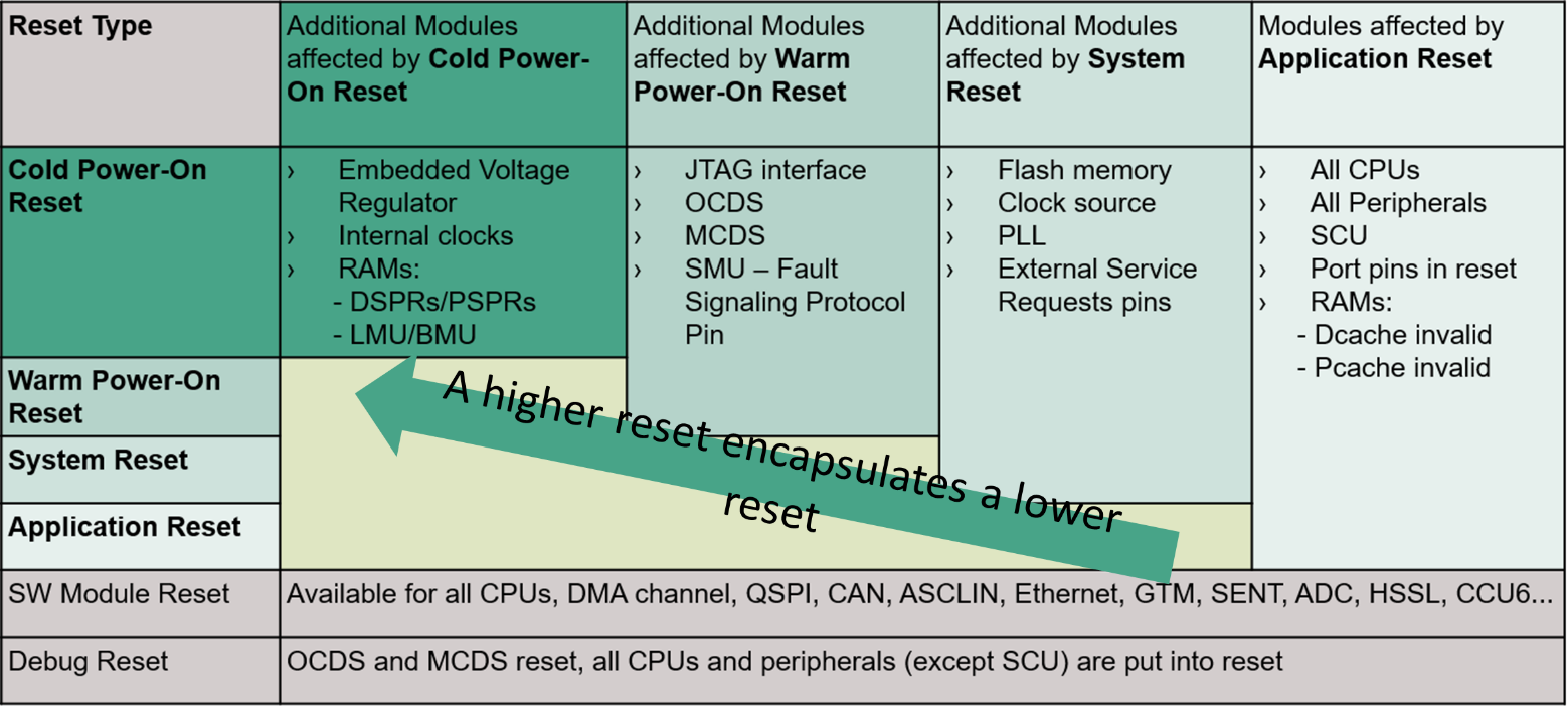
Boot and startup procedure
In this section, the startup procedure of the MCU will be explored, delving into the essential steps that occur during the device's power-on initialization. The steps that the MCU follows in an unpowered state can be divided into three different phases.
In
Figure 69
, three major sections of the startup phase are highlighted, each separated from the others by uppercase letters A, B and C. During these phases, several safety mechanisms are run to guarantee that all safety-relevant parts are working correctly. Many tests devoted to latent fault detection are also executed during this time. The following sections will report all the relevant details needed to properly understand this sequence.
Note: Phase from A to B is often referred to as startup software or "SSW".
Figure 69. Start-up sequence phases
From A to B first phase of two - analog power-up
When the external power supply reaches a specific threshold, the internal circuitry is activated and the power management system checks the 100 MHz clock. If the clock is stable, then PBIST is automatically executed.
Only if this test is successful and the VDD, VDDP3 and VEXT voltages are above the respective primary reset thresholds, PORST output is de-asserted.
This procedure is executed only if the device comes from an unpowered state (cold power-on reset); this means that for all other reset types, this phase is skipped.
From A to B second phase of two - boot firmware
Start-up configuration on AURIX™ TC3xx devices can be selected in two different ways:
Configuration by boot mode index (BMI)
According to values taken from dedicated locations in flash
The user code start address (STADD) is configurable in the boot mode header (BMHDx.STAD) data structure
Hardware configuration
Only if enabled in BMI and the HWCFG [3] pin is tied LOW
According to the values at the configuration pins
Boot mode header
The boot mode header data structure is referenced by the boot firmware and it can be used to configure the start-up behaviour of the device. In the AURIX™ TC3xx family of products, four sets of boot mode headers (BMHDx for x = 0-3) are defined in UCB to ensure boot using boot mode index (BMI). To detect data corruption, each of these data structures is replicated with its own copy. Each set, UCB_BMHDx_ORIG, has its replica as UCB_BMHDx_COPY (where x = 0-3). There must be a minimum of one set of boot mode header pairs (original and copy) programmed. Boot mode headers are stored at fixed locations within the UCB area of the data flash.
provides information on one such boot mode header data structure.
Field name | Bitfield | Description |
|---|---|---|
BMI | PINDIS bit [0] | Mode selection by configuration pins: 0 Mode selection by HWCFG pins is enabled 1 Mode selection by HWCFG pins is disabled The default use of HWCFG pins is disabled for security reasons |
HWCFG bits [3:1] | Start-up mode selection: 111 B Internal start from flash 110 B Alternate boot mode (ABM) 100 B Generic bootstrap loader (ASC/CAN BSL) 011 B ASC bootstrap loader (ASC BSL) | |
LSENA0 bit [4] | Lockstep comparator logic control for CPU0: 0 Lockstep is disabled for CPU0 1 Lockstep is enabled for CPU0 | |
LSENA1 bit [5] | Lockstep comparator logic control for CPU1: 0 Lockstep is disabled for CPU1 or not available 1 Lockstep is enabled for CPU1 | |
LSENA2 bit [6] | Lockstep comparator logic control for CPU2: 0 Lockstep is disabled for CPU2 or not available 1 Lockstep is enabled for CPU2 | |
LSENA3 bit [7] | Lockstep comparator logic control for CPU3: 0 Lockstep is disabled for CPU3 or not available 1 Lockstep is enabled for CPU3 | |
LBISTENA bit [8] | LBIST execution start with boot firmware: 0 LBIST execution is disabled 1 LBIST execution is enabled | |
CHSWENA bits [11:9] | Checker software (CHSW) execution after boot firmware: 101 B CHSW execution after boot firmware is disabled else CHSW execution after boot firmware is enabled | |
reserved bits [15:12] | ||
BMHDID | -- | Boot mode header identifier, 16-bits: B359H BMHDID OK Otherwise, BMHDID invalid |
STAD | -- | Start address (must always be inside PFlash, word-aligned), 32-bits:
Otherwise, it is not considered for mode selection |
CRCBMHD | -- | Check result for the boot mode header – 32-bit |
CRCBMHD_N | -- | Inverted check result for the boot mode header – 32-bit |
Hardware configuration pins
For start-up execution, the boot mode selection is a critical information and is configured with the boot mode index. When HWCFG pins are not connected, they represent the start-up mode as internal start from flash.
If bit PINDIS of the BMI register (see
Table 18
) is set to 0 (mode selection by HWCFG pins is enabled) and also HWCFG [3] (PORT P14.3) is 0, then the MCU will use the information present at HWCFG [4] (PORT P10.5) and HWCFG [5] (PORT P10.6) to execute boot.
HWCFG [0–2] holds the power supply hardware configuration information. HWCFG [6] decides whether port pins are by default in tri-state or behave as inputs with pull-up devices activated during and after reset. The default pull-up on HWCFG [6] ensures that all pins have a default pull-up state if this pin is left unconnected. HWCFG [6] is latched during the initial supply ramp-up.
Figure 70. Hardware configuration pins
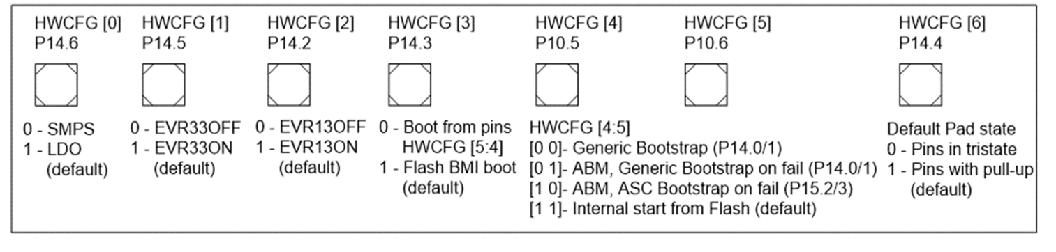
When pins HWCFG [4] and HWCFG [5] decide the boot mode of the system, the available selections are depicted in
Table 19
.
HWCFG pins | Start-up mode | |
|---|---|---|
[5] | [4] | |
1 | 1 | Internal start from flash |
1 | 0 | Alternative boot mode (ABM), generic bootstrap loader on fail |
0 | 1 | Alternative boot mode (ABM), ASC protocol bootstrap loader on fail |
0 | 0 | Generic bootstrap loader |
From B to C - application startup software
Application startup software (phase B-C) is the first code that the user can access and where initialization and init tests take place. At the end of application startup software (B-C), the program counter will jump to the first user code instruction where the “application software” execution will begin (letter C).
In the case of a restart during the application software, actions that affect the actuators outside of the MCU must only proceed after tests have been performed successfully, keeping the system in a safe state.
In AURIX™ TC3xx, the general startup sequence is defined by a few major steps that are carried out by the CPU0, which is a lockstep CPU. The entire SW startup sequence, including the evaluation of the reset cause, initialization of the hardware and startup safety tests, must be executed on a safety CPU (which is a CPU that is provided with a lockstep block).
During application startup software (B-C), the user is responsible for executing several operations to ensure the absence of latent faults and correctly initialize the MCU before starting the runtime execution. The application SW will:
Initialize the PSW register to use the interrupt stack pointer with maximum call depth counter in User-1 mode (for details see Section
TriCore™ privilege levels
). Then a reset cause evaluation is performed
Initialize the core supply (EVR) based on the external components used. Then verify the related PMS register contents against the required configured values
Execute the digital block test (LBIST) (if not already performed during FW) and evaluate the result of this test
Configure, run and check the results of secondary voltage monitors (MONBIST) to ensure the absence of latent faults in the secondary voltage monitors and standby SMU alarm path
Check the correct execution of the initial firmware (A-B phase). If something goes wrong during the A-B phase execution, then the following two possible reactions can occur:
The boot firmware stops executing and does not handover the CPU0 to the application software startup. This situation (MCU not responding) will be detected by the external watchdog
The boot firmware completes its execution, but an error is reported through one of the available error reporting interfaces. Application software is required to check the firmware error reporting interfaces before starting the safety-relevant application
Verify the correct configuration settings
The system is set up to support function calls. This includes setting up the context save area and initializing the stack pointer (A10). No global variables are used at this stage
The start-up code, depending on the application, may continue to service the internal CPU0 watchdog and safety watchdog until the watchdog is initialized by the watchdog driver. The watchdog service time is increased during start-up to slow down the watchdog and reduce overheads because of watchdog servicing. After a reset, CPU0 is in RUN mode and the CPU0 watchdog and safety watchdog start automatically. Other CPUs are initially in a HALT state and their corresponding WDTs are therefore disabled. A CPU watchdog may only be configured, enabled or disabled by its corresponding CPU
Enable, initialize and distribute the clock to the modules (that is, CPU clocks, peripheral clocks, bus clocks, pre-scalers and multipliers, which must be configured in the MCU). This includes the initialization of the PLL factors; starting the PLL lock process; and waiting until the PLL is locked
After PLL configuration, all module dividers and module clocks are re-initialized based on the configuration
The wait states for flash access will be configured into DMU_HF_DWAIT and DMU_HF_PWAIT, based on the clock setting. Right before replacing the 100 MHz backup clock with the 200 MHz ... 300 MHz PLL clock, it must increase the number of wait states of the flash. The pre-fetch buffer and the branch predictor also need to be activated
Test the functionality of the SMU core alive monitor and the reaction in the stand-by SMU by injecting an error and checking the result
Execute tests of all safety-relevant functional blocks (tests of diagnostic modules). During the initial safety test and initialization phase, it may be required to service the watchdogs in between, depending on the time taken for the tests
Configure (in non-destructive mode), run and check the result of the variable memory test (MBIST) to ensure the absence of faults in RAM
Ensure to enable all SMU alarms relevant for the application. In particular, the user will re-enable alarms that were disabled during the oscillator and PLL configuration procedures
Initialization of other peripherals and common resources
Initialization of ports and pins: Here, the required initial state is imposed
Setting up the system to support interrupt and trap mechanisms (Initializing BIV and BTV registers, which set interrupt and trap vector tables)
Initializing global variables for CPU0 and CPU Shared variables
Starting the additional CPUs as configured. Multi-core start-up occurs in a daisy chain sequence, where one CPU enables the next CPU in the sequence. Steps
7
,
8
and
18
are executed for each CPU depending on what is applicable
The next step is the transfer of control to OS
The one reported here is a general structure of the initialization sequence and several changes can be made to adapt it to the specific use case.
A test of "primary monitors" (to detect latent faults) can be conducted at start-up in case the run-time operation takes a maximum of a well-defined number of hours (for example, driving cycle time up to a maximum of 12 hours for automotive and 24 hours for domestic appliances). In case the time before a cold power-on reset is expected to be longer, a latent faults test will be executed at startup (B-C phase above), but it can be useful to replicate part of them in the run-time software. In this last case, attention should be paid not to interfere too much with the program’s normal execution by distributing the tests in time slots or creating a run-time version of them.
Run-time single-point fault tests
Run-time single-point fault tests are those that need to be executed "continuously" during application software (in the case of hardware-built-in tests such as ECC and EDC) or need to be executed within the fault detection time interval (FDTI).
Examples of these run-time tests are:
Interrupt service requests monitoring
Port loop back reading
Program flow monitoring
Plausibility checks
Error handling
Before discussing about error handling, it is important recapping the following definitions:
Fault
: An abnormal condition that can cause an element or an item to fail.
Error
: Discrepancy between a computed, observed or measured value or condition and the true, specified or theoretically correct value or condition.
Failure
: Termination of the ability of an element to perform a function as required.
Figure 71. Fault, Error, and Failure
The focus is on errors as the difference between a measured condition and a theoretically correct one.
The possible error sources are:
Application software checks
CPUs
Peripheral blocks hardware safety mechanisms
Errors in AURIX™ TC3xx are handled in different ways depending on the following three main error sources:
Application software errors
Application software errors are those raised by plausibility checks, test routines, or monitoring functions that are part of the specific customer software implementation.
Traps handled errors
The primary feature for handling errors on the TriCore™ cores is trap handlers. Errors such as illegal OP-codes and memory address, that have been caused and detected by one of the cores, trigger a trap. Whenever a trap is triggered, the core will call user-defined trap handlers. On the cores of the AURIX™ TC3xx, there are 8 different classes of traps, each with a different trap handler.
Note: More details are in the TriCore™ TC1.6.2 core architecture manual, vol.1, Section 6.
SMU handled errors
As shown in
Figure 72
, in AURIX™ TC3xx, there are peripheral hardware errors that occur in a more global scope with respect to the core itself, such as bit flips in memory or overheating of the die. Those error-detection mechanisms have a direct connection to the SMU of the AURIX™ TC3xx and are connected to SMU alarms.
Moreover, there are CPU errors, such as access rights violations in the memory protection unit (MPU) of the CPU, that cause a trap whose trap handler triggers an SMU alarm. The user can also trigger dedicated custom software (SW) alarms to the SMU coming from application errors (sensors, output drivers).
Figure 72. Error handling simplified scheme for AURIX™ TC3xx
Multicore aspects
Many embedded systems exploit the benefits of multi-core MCUs distributing the workload over different cores, enhancing performances with acceptable power consumption to implement various functionalities.
Programming multi-core applications is challenging because developers of embedded software must deal with the complexity of such a kind of architecture and, at the same time, they face increasing requirements on functional safety in both industrial and automotive application fields.
AURIX™ TC3xx is an actual multicore MCU. A safety multicore needs robust partitioning under different aspects:
Data partitioning
is robust when the software running on each core exclusively uses the system data and program memory areas
Time partitioning
is achieved when the software running on each core uses system resources within its own dedicated time slots only
Resources partitioning
is robust when the software running on each core uses exclusively the system hardware resources (peripherals)
To reach robust partitioning, it is needed to identify:
The software architecture to be used.
All the software “safety functions” that will be hosted on the MCU.
How software functions will interact with each other (based on the freedom from interference concept explained in Section
Freedom from interference (FFI)
).
Freedom from interference (FFI)
To prevent safety applications with different safety goals interacting with each other, AURIX™ TC3xx devices implement a number of hardware features, allowing them to isolate hardware and software components that are not meant to interfere. A simplified example of “isolation” is represented in
Figure 73
.
In the following sections, an overview of these protection mechanisms is given. It is the user’s responsibility to configure them as per the needs of the safety application.
To ensure the independence between an ASIL function and a QM function, freedom from interference must be achieved in the data, resource and time domains to avoid the following situations:
A hardware/software element corrupts data belonging to another hardware/software element (data domain)
A hardware/software element consumes too much CPU performance or uses a shared resource (internal bus, peripherals, communication network) for a long time, preventing other elements from reaching their execution latency requirements (time domain)
A hardware/software element uses or modifies the configuration of a resource (internal bus, peripheral, communication network) belonging to another application (resource domain)
Figure 73. Example of freedom from interference realization
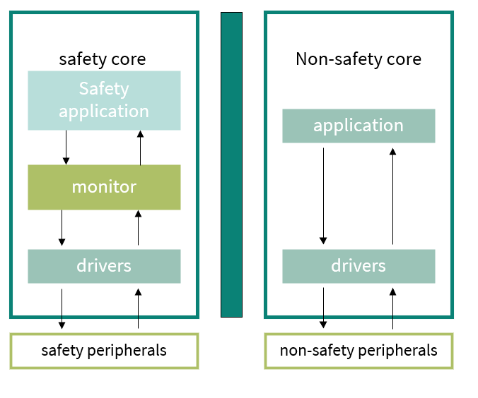
To ensure freedom from interference from a generic element (hardware or software), it is possible to utilize the AURIX™ TC3xx MCU family features.
Data domain
In the context of embedded systems, the data domain of a specific core can be accessed and shared within the system. It is important to define which parts of the data or memory are exclusively accessible by a particular core (private data) and which parts are shared among multiple cores (shared data). Managing the data domain in embedded systems is crucial for maintaining data consistency, avoiding data conflicts and ensuring efficient inter-core communication.
Memory protection system of the TriCore™ CPU
To implement freedom from interference between software components in the data domain, memory partitioning is generally used. Memory protection in the TriCore™ CPU is facilitated by the robust memory protection system. This safety-relevant feature extends its functionality to both data memory and program memory, offering safeguards against unauthorized read, write or instruction fetch accesses by software running on the CPU.
In the TriCore™ version embedded in the AURIX™ TC3xx MCU (revision 1.6.2), there are six available memory protection register sets. The PSW.PRS bit field (in the range 0-5) determines which of these sets is currently in use by the CPU, as depicted in
Figure 74
.
The CPU's memory protection system operates as a hardware mechanism, providing range-based protection for program memory and data memory. Each protection range is a contiguous part of the address space, precisely defined by lower and upper boundaries, wherein access permissions are specified.
The protection sets are used, in turn, to determine data access and instruction-fetch permissions. The hardware efficiently manages the changing of protection sets during task context switches, ensuring seamless protection and allocation of code execution ranges as well as data ranges. This comprehensive approach guarantees the integrity of the embedded system's memory architecture.
The memory protection is disabled after a reset and no protection ranges are defined. The application must initialize the protection ranges and permissions, adapting them to the software architecture. A few safety operating systems enable this protection immediately after the startup phase.
Several data and code ranges (represented by the blocks called "data regions" and "code regions" in
Figure 74
) can be defined based on the upper and lower boundary registers of each region. Once those regions are set up, a register set (DPRE, DPWE and CPXE) can be associated with some of the available regions by setting the bits corresponding to the read permission enabled data, write permission enabled data and execute permission enabled code for that specific memory region.
Note: More details are in the TriCore™ TC1.6.2 core architecture manual, vol.1, Section 10.
Figure 74. CPU memory protection system usage
Bus memory protection
Each CPU's memory is also accessible to all bus masters, such as CPUs and DMA. To avoid interference from other bus masters, each shared memory implements a region access protection mechanism. The mechanism, identified as bus memory protection of the CPU, is a hardware mechanism that protects user-specified memory ranges of the CPU's local memories (DSPR, PSPR, DLMU and NVM) from unauthorized write accesses through the SRI slave interface. To implement this mechanism, the system integrator must define the upper and lower boundaries (RGNUA and RGNLA) of a few regions to which some masters can access and others cannot (RGNACCENA and RGNACCENB).
Figure 75. Bus memory protection usage
Using this method, the system integrator can restrict, for example, write access from CPU0 to CPU1 DSPR to a dedicated memory region of DSPR used as a communication buffer between the two cores. Similarly, this mechanism can restrict write access from DMA channels.
For each memory range, one or more masters can be authorized. This mechanism supports the following complex bus memory protection schemes:
Only specifically identified software (safe software) is allowed to write to a region
Only specifically identified DMA channels are allowed to write to a region
Bus memory protection initialization
: After reset, the bus memory protection allows access to the entire addressable space for all masters. The application must initialize the protection ranges and permissions adapted to the software architecture. A few safety operating systems enable this protection immediately after the startup phase.
Note: More details are in the TriCore™ TC1.6.2 core architecture manual, vol.1, Section 10.
Time domain
The AURIX™ TC3xx MCU provides a set of hardware functions that enable the application to verify that the static timing properties of the safety-related tasks are met during run-time. Two ways of accomplishing the time monitoring function are available:
Watchdogs
To support time monitoring, MCU provides internal watchdogs. There is one internal watchdog per CPU plus one safety watchdog for the entire MCU
Temporal protection system
The TriCore™ also implements a temporal protection system to guard against run-time overruns. The system consists of two primary mechanisms:
Temporal protection timers
Exception timers
The temporal protection timer system consists of three independent decrementing 32-bit counters, arranged to generate a temporal asynchronous exception (TAE) trap on decrement to zero. On the other side, the exception timer system provides a method of detecting the overrun of exception handlers in the system.
Note: More details are in the TriCore™ TC1.6.2 core architecture manual, vol.1, Section 11.
Resource domain
To control access to their resources and provide freedom from interference in the resource domain, AURIX™ TC3xx modules implement various useful features.
Figure 76. Protection of peripheral resources
Register access protection (AP)
Each on-chip resource with direct or indirect bus master capability has a unique master TAG ID that can be used to identify the master of an on-chip bus transaction. TAG_ID-based protection means that on-chip bus write access to the control registers can be disabled for each master TAG_ID individually. For a disabled master TAG_ID, write access will be disconnected with an error acknowledgement. However, read access will be processed.
This identifier allows each bus slave to select which master is allowed to access its resources. For example, a QSPI peripheral block can be configured in such a way that CPU1 (the master) has no access to its registers. Access to the registers of a functional block (slave) of the MCU is limited by their ACCEN registers, which will set the TAG ID for the masters to which they will be granted the possibility to modify the block registers.
In addition, the access enable registers (ACCEN1/0) are "Safe Endinit" protected. After reset, all ACCEN1/0 access enable bits and access control bits are enabled and access protection mechanisms must be configured and checked to bring the system to a safe state.
TriCore™ privilege levels
The TriCore™ privilege levels control access to peripheral devices and special function registers. Each CPU task or DMA channel is allocated a privilege level, which can be:
User-0 mode
No peripheral access. Access to memory regions with the peripheral space attribute is prohibited and results in a trap. This access level is given to tasks that do not directly access peripheral devices. Tasks at this level do not have permission to enable or disable interrupts
User-1 mode
Regular peripheral access enables access to common peripheral devices that are not specially protected, including read/write access to serial I/O ports, read access to timers and access to most I/O status registers. Tasks at this level may disable interrupts
Supervisor mode
Enables access to all peripheral devices. It enables read/write access to core registers and protected peripheral devices. Tasks at this level may disable interrupts
This feature gives the possibility that only masters with supervisor mode access (in write mode) critical resources, since write accesses to protected registers performed by masters configured in user mode will result in activating alarms to the SMU.
CPU Endinit protection
There are several registers in the TC3xx that are usually programmed only once during the initialization sequence of the system or application. Modification of such registers during a normal application run can have a severe impact on the overall operation of modules or the entire system. While the supervisor mode and the access protection scheme provide a certain level of protection against unintentional modifications, they may not be sufficient to protect against all unintended accesses to system-critical registers.
The AURIX™ TC3xx provides one more level of protection for such registers via the various Endinit features. This is a highly secure write-protection scheme that makes unintentional modifications of registers protected by this feature impossible. Writes are only enabled if the corresponding ENDINIT bit is 0 and supervisor mode is active. Write attempts if this condition is not true will be discarded and the register contents will not be modified in this case. The bus control unit (BCU) controls the operation following a discarded write access and triggers an alarm to SMU.
In addition, each WDT monitors ENDINIT bit modifications by starting a time-out sequence each time software opens access to the critical registers through clearing the corresponding ENDINIT bit. If the time-out period ends before the corresponding ENDINIT bit is set again, a malfunction of the software is assumed and a watchdog fault response is generated. A user-defined password is needed to de-activate the ENDINIT protection and then access critical registers.
Note: Every CPU has its own ENDINIT mechanism, which also means a dedicated watchdog.
Safety Endinit protection
Similarly to the CPU Endinit functionality, which is handled by the CPU watchdogs, the safety watchdog also allows to protect a set of safety-related registers via a safety Endinit locking scheme.
Note: More details about Endinit functions can be found in AURIX™ TC3xx User’s Manual v2.0, vol. 1.
In summary, both Endinit and safety Endinit are mechanisms that contribute to the overall robustness and security of the AURIX™ TC3xx MCU. They help to prevent accidental or malicious alterations to critical settings, ensuring stable and secure operation, with safety Endinit providing an even higher level of protection suitable for safety-critical applications.
Alarm test mechanism
Motivation for this section is that the existing alarm test mechanisms are often challenging to use, and not every hardware mechanism has a corresponding alarm test mechanism.
Many customers test alarms to verify the application's reaction during development.
To accomplish that, it is possible to simply leave the SMU in START state, and verify each alarm reaction by invoking each alarm with a write to SMU_AGx.
It is important to understand that latent random faults in digital blocks within AURIX™ TC3xx logic are mainly addressed by the LBIST and other runtime safety mechanisms and do not require additional alarm tests.
Available AURIX™ TC3xx software
The software development can be done fully in-house or partially using software libraries offered by Infineon or Infineon partners.
shows a brief overview of what Infineon or its partners offer today.
Figure 77. Example of embedded software offered by Infineon or its partners
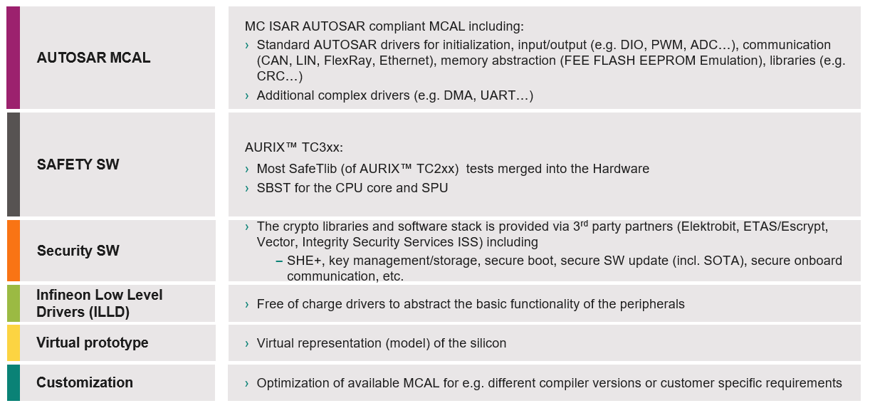
References
Infineon Technologies AG:
AURIX™ TC3xx User's Manual V2.0.0
; 81726 Munich; 2021-02; Available online
Infineon Technologies AG::
TriCore™ TC1.6.2 core architecture manual
; Available online
ISO 26262:2018 Road vehicles- Functional safety
; Available online
IEC 61508:2010 Functional safety of electrical/electronic/programmable electronic safety-related systems
; Available online
Glossary
Definition | Description | Notes |
|---|---|---|
ASC | Active Short Circuit | in the Inverter Use Case |
Architectural Element | The smallest element on which the FMEDA is performed | |
ASIL | Automotive Safety Integrity Level; refer to ISO 26262-1:2018, 3.6 | |
BEV | Battery-powered Electric Vehicle | |
CCF | Common-Cause Failure; refer to ISO 26262-1:2018, 3.18 | |
DC | Diagnostic Coverage; refer to ISO 26262-1:2018, 3.33 | |
DFA | Dependent Failure Analysis identifies single events that can cause multiple sub-parts to malfunction (for example, intended function and its safety mechanism) and lead to a violation of a safety requirement or safety goal. | |
DMI | Data Memory Interface | |
DPF | Dual-Point Failure; for the definition refer to ISO 26262-1:2018, clause 3.38 | |
DSPR | Data Scratch Pad RAM | |
ECU | Electronic Control Unit | |
FHTI | Fault Handling Time Interval is defined in ISO 26262 as the sum of three elements: The fault detection time, the fault reaction time and the time for the system to reach a safe state. | |
FTTI | Fault Tolerant Time Interval; for the definition refer to ISO 26262-1:2018, clause 3.61 | |
FMEA | Failure Mode and Effects Analysis | |
FMEDA | Failure Modes, Effects and Diagnostic Analysis Analysis of the effect of random hardware faults on a safety requirement or safety goal, including quantitative estimation of failure rates and the probability/rate of a safety goal violation | Quantitative Bottom-up HW only |
FTA | Fault Tree Analysis Analysis in which a top-level failure mode is broken down to a combination of lower-level faults (root causes) using a Boolean logic approach | Qualitative (may be quantitative) Top-down HW only |
HARA | Hazard Analysis and Risk Assessment; Refer to ISO 26262-1:2018, 3.76 | |
HW | Hardware | |
IC | Integrated Circuit | |
IEC | International Electrotechnical Commission | |
ISO | International Organization for Standardization | |
LBIST | Logic Built-in Self Test | |
LMU | Local Bus Memory Unit | |
MCU | Microcontroller unit | |
MMIC | Monolithic Microwave Integrated Circuit is a type of integrated circuit (IC) device that operates at microwave frequencies (300 MHz to 300 GHz). These devices typically perform functions such as microwave mixing, power amplification, low-noise amplification and high-frequency switching. | |
PMI | Program Memory Interface | |
PMIC | Power Management ICs (PMICs) | |
PMSM | Permanent Magnet Synchronous Machine (with rare earth material) | Motor type |
PSPR | Program Scratch Pad RAM | |
Safety Flip Flops (SFF’s) | Safety flip-flops are special flip-flops that implement a hardware mechanism capable of detecting bit flips within the protected registers, thus preventing single-point faults. | |
Safety Measure | Activity or technical solution to prevent, detect, control or mitigate systematic and random failures. | |
SBC | system basis chips (SBC) SBCs combine mainly three functionalities in a single device: Power supply, CAN and/or LIN transceivers and supporting features (MCU supervision, SPI interface and so on). This integration makes SBC a potentially better alternative to standalone (discrete) solutions, especially in terms of total solution cost and total area. | |
SE | Soft Error | |
SM | Safety Mechanism: for the definition refer to ISO 26262-1:2018, 3.142 | |
SW | Software | |
SPU | Signal Processing Unit | |
STP | Shoot-Through Protection: Protection typical of an inverter gate driver so that the high side and the low side of the three-phase motor legs cannot be activated simultaneously | |
VCU | Vehicle Control Unit |
Revision history
Document revision | Date | Description of changes |
|---|---|---|
V1.0 | 2023-12-18 | Initial release |
V1.1 | 2024-02-14 | Standard references added in Table 1 Detailed standard references added in section ISO 26262 perspective and IEC 61508 perspective Reformat of Figure 72 and Figure 73 Removed subchapter 7.8 "Short view on operating systems" Standard references added in owq1745576218449.html#ibh1743157773785__table_hww_fsn_v2c |
V1.2 | 2024-04-16 | Added information about Lockstep CPUs RAM instances in clause CPU RAMs Corrected Figure 55 about XEV traction inverter Added explicit reference to SMU alive monitor test in section From B to C - application startup software Added some details on verification of SMU alarm reaction in section Alarm test mechanism updated |
V1.3 | 2025-05-26 | Template update; no content update |
1
Even if it is possible to connect IHx_N and ILx to the same MCU pin because the gate driver itself provides the negation of IHx_N with respect to ILx, for better performances, it is preferable to keep IHx_N not connected to ILx so that dead time can be customized.