AN1200 FuSa in a Nutshell - Safety software enablement with AURIX™ TC3xx
32-bit TriCore™
AURIX™ TC3xx microcontroller
About this document
Scope and purpose
As requirements from functional safety standards in automotive, industrial and other fields are a challenging subject, this document intends to provide a first set of guidelines for users who are unfamiliar using the AURIX™ TC3xx microcontroller unit (MCU) in a functional safety scope.
This application note is part of a series of document named "FuSa in a nutshell"as listed in
3
.
Intended audience
This document is intended for all those evaluating the AURIX™ TC3xx MCU, including functional safety engineers on the customer side and application engineers. This includes designers of safety-related systems who:
Are new to functional safety
Want to know more about functional safety (also called “FuSa”) applications
Want to understand in principle how functional safety can be implemented with hardware support
Are looking for functional safety details that cannot be found in the MCU user manual
Structure of the document
This document wants to provide a first guidance on the following safety related arguments:
MCU initialization
Software fault reactions
How to use multicore architecture in the best way
How to organize safety and non-safety code partitioning considering freedom from interference aspects
Disclaimer
Information included in this document is for training purposes only and should not to be taken as a blueprint for productive development.
Introduction
The AURIX™ TC3xx features enable customers to develop application software up to the most stringent safety standards, effectively meeting all specified requirements. Functional safety software will mainly guarantee two aspects:
The safety of the SEooC itself
The safety of the function that is intended to be implemented with the help of the MCU
This means that parts of the safety code will be necessary to complete the safety tests of the internal blocks of the MCU (for example, fault injections, clock plausibility, ADC voltage reference test and so on) and parts of the safety code will be in charge of implementing the application-specific safety functions.
All this safety code needs to be inserted into a well-structured architecture. When starting with the task of designing the software architecture, the initial set of inquiries that need answers may include:
How to perform initialization (which MCU core should start, what to do later, when enabling interrupts and what to do when coming from standby)
How to react to a fault (types of possible reactions and, in the case of a reset reaction, what kind of reset and so on)
How to use multicore architecture in the best way
How to organize safety and non-safety code partitioning (data protection, program protection, temporal protection) considering freedom from interference aspects
In the following sections, these points will be analyzed deeply, allowing the reader to understand how the AURIX™ MCU can fulfil the earlier mentioned topics.
MCU operating modes
One of the features of the MCU is its ability to operate in different modes, which allows it to adapt to various requirements and efficiently manage power consumption. These operating modes enable MCUs to balance performance with energy efficiency, making them suitable for a wide range of applications. By utilizing different modes, developers can optimize the behavior of an MCU, ensuring it meets the specific needs of their embedded systems without removing power when not necessary, and enhancing the overall performance.
At any point in time, the MCU will be in one of the following modes:
Completely unpowered
The MCU is not supplied and no energy is provided to the device. No internal circuitry is active
Reset mode
While in this state, the I/O pins are in a reset state and the internal modules are kept in a known state and are inactive
Power-up mode
When the voltage supplies reach a certain threshold, the internal circuitry is activated and all modules and memories are initialized. If initial tests are successful, CPU0 is released from reset and the startup software is executed. During this phase, the safety mechanisms are initialized and tested by the startup software
Run mode
If all tests are successful, the CPU0 releases the other CPU and the application software is executed. All necessary safety mechanisms are supposed to be active, even those that require software configuration. This is the normal state of the MCU during operation
Internal error mode
Because of an internal failure, the MCU outputs are potentially dangerous. The user can configure the dedicated FSP error pin to signal this state so that the "secondary safety path" can be activated
Standby mode
This mode is entered on a SW request or because of an ESR1 assertion event. In this mode, only the standby controller and the wake-up unit are active. All other peripherals and CPUs are switched off. Ports are set to their default state. No safety mechanisms are active
Sleep mode
This mode is entered by SW request. CPU code execution is halted and CPUs are held in an idle state. Peripherals are in a sleep state and ports keep their programmed value. No safety mechanisms are active in the "sleeping" blocks
Debug mode
This mode is enabled to allow the developer to access HW registers and functions during the development phase. In debug mode, the safety mechanisms are active, but there is no guarantee that the debug module (OCDS) in the device will not interfere with the HW. Therefore, no safety-relevant applications should run in this mode
The only mode assumed in the safety concept of the MCU is run mode.
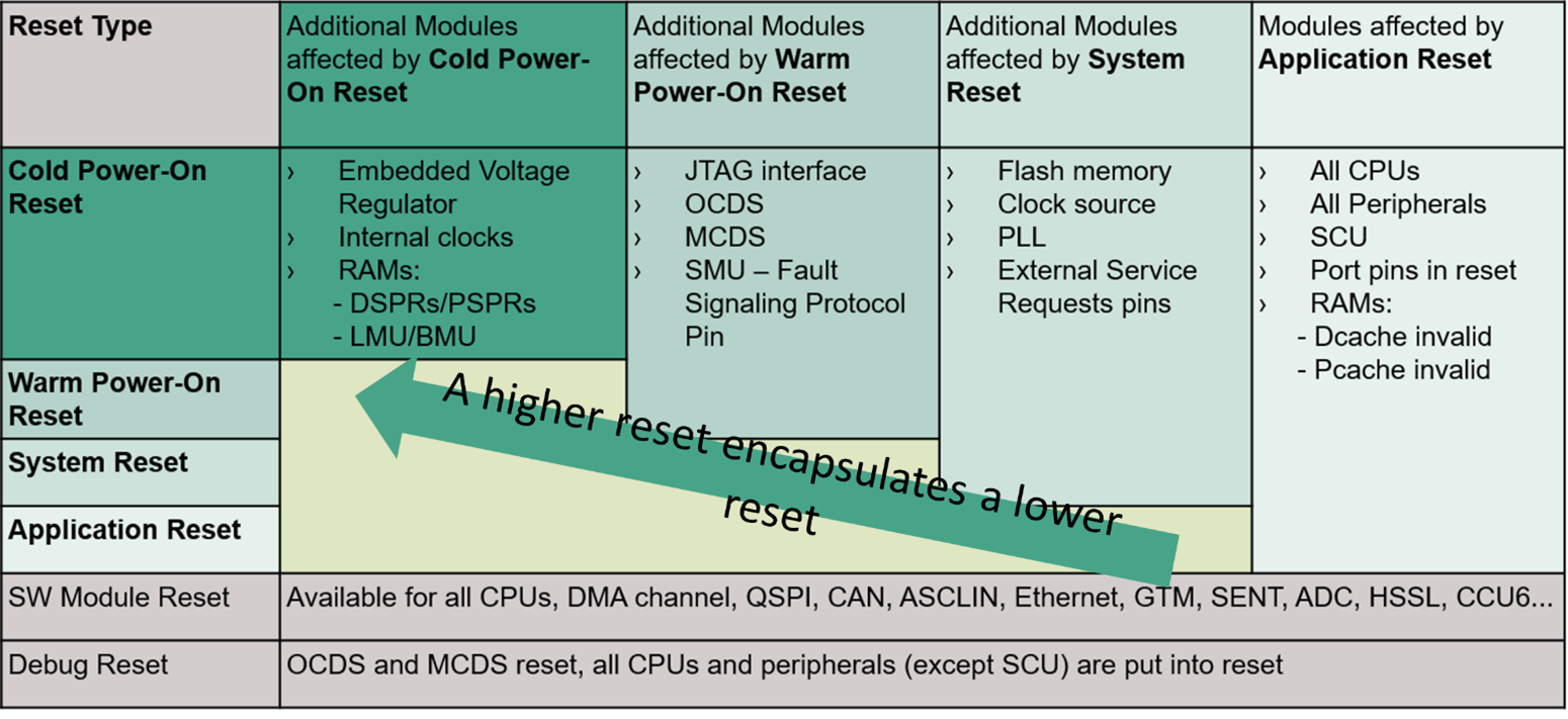
Types of resets
AURIX™ TC3xx has a scalable reset concept, where different types of resets are encapsulated one into the other. The cold power-on reset is the highest reset type, where the embedded voltage regulator (EVR), internal clocks and RAMs are reset in addition to the modules affected by the application reset, system reset and warm power-on reset. In addition to the resets affecting all the modules, there are also SW module reset and debug reset that enable the user to directly trigger a reset of the connected modules.
Depending on the number of modules involved in the reset, the following are the different kinds of resets:
Cold Power-On Reset
A Cold Power-On Reset is a reset that is triggered for the first time during a system power-up or in response to a temporary power failure. The pins and internal states are placed immediately into their default state when the trigger is asserted. The system is placed in a defined state and all registers keep their reset values as long as the reset is asserted. Data scratch pad RAM (DSPR), program scratch pad RAM (PSPR) and local bus memory unit (LMU) are re-initialized only after a cold power-on reset. In all other reset types, their content and redundancy are not affected
Warm Power-On Reset
A warm reset is triggered while the system is already operational and the supplies remain stable. It is used to return the system to a known state. On a warm reset request, port pins are immediately placed in the default state and all internal peripherals and the CPU are re-initialized. PORST pin assertion keeps the MCU in warm power-on reset type
System Reset
As for the Warm Power-on Reset, this reset leads to an initialization into a defined state of the complete system. This type of reset can be triggered intentionally by the application software by configuring specific registers
Application Reset
This reset leads to an initialization into a defined state of the complete application system, which means all peripherals, all CPUs, all pins and part of the SCU. As for system reset, application software can configure the trigger sources
Module Reset
Individual reset commands can be sent by authorized masters to a single module without any impact on the rest of the system
shows the different kinds of resets and their effects on the various parts of the MCU.
Figure 1. Different kinds of resets and their effects on the various parts of the MCU
Boot and startup procedure
In this section, the startup procedure of the MCU will be explored, delving into the essential steps that occur during the device's power-on initialization. The steps that the MCU follows in an unpowered state can be divided into three different phases.
In Figure 2, three major sections of the startup phase are highlighted, each separated from the others by uppercase letters A, B and C. During these phases, several safety mechanisms are run to guarantee that all safety-relevant parts are working correctly. Many tests devoted to latent fault detection are also executed during this time. The following sections will report all the relevant details needed to properly understand this sequence.
Note: Phase from A to B is often referred to as startup software or "SSW".
Figure 2. Start-up sequence phases
From A to B first phase of two - analog power-up
When the external power supply reaches a specific threshold, the internal circuitry is activated and the power management system checks the 100 MHz clock. If the clock is stable, then PBIST is automatically executed. Only if this test is successful and the VDD, VDDP3, and VEXT voltages are above the respective primary reset thresholds, PORST output is de-asserted.
This procedure is executed only if the device comes from an unpowered state (cold power-on reset); this means that for all other reset types, this phase is skipped.
From A to B second phase of two - boot firmware
Start-up configuration on AURIX™ TC3xx devices can be selected in two different ways:
Configuration by boot mode index (BMI)
According to values taken from dedicated locations in flash
The user code start address (STADD) is configurable in the boot mode header (BMHDx.STAD) data structure
Hardware configuration
Only if enabled in BMI and the HWCFG [3] pin is tied LOW
According to the values at the configuration pins
Boot mode header
The boot mode header data structure is referenced by the boot firmware and it can be used to configure the start-up behaviour of the device. In the AURIX™ TC3xx family of products, four sets of boot mode headers (BMHDx for x = 0-3) are defined in UCB to ensure boot using boot mode index (BMI). To detect data corruption, each of these data structures is replicated with its own copy. Each set, UCB_BMHDx_ORIG, has its replica as UCB_BMHDx_COPY (where x = 0-3). There must be a minimum of one set of boot mode header pairs (original and copy) programmed. Boot mode headers are stored at fixed locations within the UCB area of the data flash.
provides information on one such boot mode header data structure.
Field name | Bitfield | Description |
|---|---|---|
BMI | PINDIS bit [0] | Mode selection by configuration pins: 0 Mode selection by HWCFG pins is enabled 1 Mode selection by HWCFG pins is disabled The default use of HWCFG pins is disabled for security reasons |
HWCFG bits [3:1] | Start-up mode selection: 111 B Internal start from flash 110 B Alternate boot mode (ABM) 100 B Generic bootstrap loader (ASC/CAN BSL) 011 B ASC bootstrap loader (ASC BSL) | |
LSENA0 bit [4] | Lockstep comparator logic control for CPU0: 0 Lockstep is disabled for CPU0 1 Lockstep is enabled for CPU0 | |
LSENA1 bit [5] | Lockstep comparator logic control for CPU1: 0 Lockstep is disabled for CPU1 or not available 1 Lockstep is enabled for CPU1 | |
LSENA2 bit [6] | Lockstep comparator logic control for CPU2: 0 Lockstep is disabled for CPU2 or not available 1 Lockstep is enabled for CPU2 | |
LSENA3 bit [7] | Lockstep comparator logic control for CPU3: 0 Lockstep is disabled for CPU3 or not available 1 Lockstep is enabled for CPU3 | |
LBISTENA bit [8] | LBIST execution start with boot firmware: 0 LBIST execution is disabled 1 LBIST execution is enabled | |
CHSWENA bits [11:9] | Checker software (CHSW) execution after boot firmware: 101 B CHSW execution after boot firmware is disabled else CHSW execution after boot firmware is enabled | |
reserved bits [15:12] | ||
BMHDID | -- | Boot mode header identifier, 16-bits: B359H BMHDID OK Otherwise, BMHDID invalid |
STAD | -- | Start address (must always be inside PFlash, word-aligned), 32-bits:
Otherwise, it is not considered for mode selection |
CRCBMHD | -- | Check result for the boot mode header – 32-bit |
CRCBMHD_N | -- | Inverted check result for the boot mode header – 32-bit |
Hardware configuration pins
For start-up execution, the boot mode selection is a critical information and is configured with the boot mode index. When HWCFG pins are not connected, they represent the start-up mode as internal start from flash.
If bit PINDIS of the BMI register (see
Table 1
) is set to 0 (mode selection by HWCFG pins is enabled) and also HWCFG [3] (PORT P14.3) is 0, then the MCU will use the information present at HWCFG [4] (PORT P10.5) and HWCFG [5] (PORT P10.6) to execute boot.
HWCFG [0–2] holds the power supply hardware configuration information. HWCFG [6] decides whether port pins are by default in tri-state or behave as inputs with pull-up devices activated during and after reset. The default pull-up on HWCFG [6] ensures that all pins have a default pull-up state if this pin is left unconnected. HWCFG [6] is latched during the initial supply ramp-up.
Figure 3. Hardware configuration pins
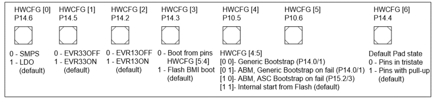
When pins HWCFG [4] and HWCFG [5] decide the boot mode of the system, the available selections are depicted in
Table 2
.
HWCFG pins | Start-up mode | |
|---|---|---|
[5] | [4] | |
1 | 1 | Internal start from flash |
1 | 0 | Alternative boot mode (ABM), generic bootstrap loader on fail |
0 | 1 | Alternative boot mode (ABM), ASC protocol bootstrap loader on fail |
0 | 0 | Generic bootstrap loader |
From B to C - application startup software
Application startup software (phase B-C) is the first code that the user can access and where initialization and init tests take place. At the end of application startup software (B-C), the program counter will jump to the first user code instruction where the "application software" execution will begin (letter C).
In the case of a restart during the application software, actions that affect the actuators outside of the MCU must only proceed after tests have been performed successfully, keeping the system in a safe state.
In AURIX™ TC3xx, the general startup sequence is defined by a few major steps that are carried out by the CPU0, which is a lockstep CPU. The entire SW startup sequence, including the evaluation of the reset cause, initialization of the hardware and startup safety tests, must be executed on a safety CPU (which is a CPU that is provided with a lockstep block).
During application startup software (B-C), the user is responsible for executing several operations to ensure the absence of latent faults and correctly initialize the MCU before starting the runtime execution. The application SW will:
Initialize the PSW register to use the interrupt stack pointer with maximum call depth counter in User-1 mode (for details see Section
TriCore™ privilege levels
). Then a reset cause evaluation is performed
Initialize the core supply (EVR) based on the external components used. Then verify the related PMS register contents against the required configured values
Execute the digital block test (LBIST) (if not already performed during FW) and evaluate the result of this test
Configure, run and check the results of secondary voltage monitors (MONBIST) to ensure the absence of latent faults in the secondary voltage monitors and standby SMU alarm path
Check the correct execution of the initial firmware (A-B phase). If something goes wrong during the A-B phase execution, then the following two possible reactions can occur:
The boot firmware stops executing and does not handover the CPU0 to the application software startup. This situation (MCU not responding) will be detected by the external watchdog
The boot firmware completes its execution, but an error is reported through one of the available error reporting interfaces. Application software is required to check the firmware error reporting interfaces before starting the safety-relevant application
Verify the correct configuration settings
The system is set up to support function calls. This includes setting up the context save area and initializing the stack pointer (A10). No global variables are used at this stage
The start-up code, depending on the application, may continue to service the internal CPU0 watchdog and safety watchdog until the watchdog is initialized by the watchdog driver. The watchdog service time is increased during start-up to slow down the watchdog and reduce overheads because of watchdog servicing.
After a reset, CPU0 is in RUN mode and the CPU0 watchdog and safety watchdog start automatically. Other CPUs are initially in a HALT state and their corresponding WDTs are therefore disabled. A CPU watchdog may only be configured, enabled or disabled by its corresponding CPU
Enable, initialize and distribute the clock to the modules (that is, CPU clocks, peripheral clocks, bus clocks, pre-scalers and multipliers, which must be configured in the MCU). This includes the initialization of the PLL factors; starting the PLL lock process; and waiting until the PLL is locked
After PLL configuration, all module dividers and module clocks are re-initialized based on the configuration
The wait states for flash access will be configured into DMU_HF_DWAIT and DMU_HF_PWAIT, based on the clock setting. Right before replacing the 100 MHz backup clock with the 200 MHz ... 300 MHz PLL clock, it must increase the number of wait states of the flash. The pre-fetch buffer and the branch predictor also need to be activated
Test the functionality of the SMU core alive monitor and the reaction in the stand-by SMU by injecting an error and checking the result
Execute tests of all safety-relevant functional blocks (tests of diagnostic modules). During the initial safety test and initialization phase, it may be required to service the watchdogs in between, depending on the time taken for the tests
Configure (in non-destructive mode), run and check the result of the variable memory test (MBIST) to ensure the absence of faults in RAM
Ensure to enable all SMU alarms relevant for the application. In particular, the user will re-enable alarms that were disabled during the oscillator and PLL configuration procedures
Initialization of other peripherals and common resources
Initialization of ports and pins: Here, the required initial state is imposed
Setting up the system to support interrupt and trap mechanisms (Initializing BIV and BTV registers, which set interrupt and trap vector tables)
Initializing global variables for CPU0 and CPU Shared variables
Starting the additional CPUs as configured. Multi-core start-up occurs in a daisy chain sequence, where one CPU enables the next CPU in the sequence. Steps
7
,
8
and
18
are executed for each CPU depending on what is applicable
The next step is the transfer of control to OS
The one reported here is a general structure of the initialization sequence and several changes can be made to adapt it to the specific use case.
A test of "primary monitors" (to detect latent faults) can be conducted at start-up in case the run-time operation takes a maximum of a well-defined number of hours (for example, driving cycle time up to a maximum of 12 hours for automotive and 24 hours for domestic appliances).
In case the time before a cold power-on reset is expected to be longer, a latent faults test will be executed at startup (B-C phase above), but it can be useful to replicate part of them in the run-time software. In this last case, attention should be paid not to interfere too much with the program’s normal execution by distributing the tests in time slots or creating a run-time version of them.
Run-time single-point fault tests
Run-time single-point fault tests are those that need to be executed "continuously" during application software (in the case of hardware-built-in tests such as ECC and EDC) or need to be executed within the fault detection time interval (FDTI).
Examples of these run-time tests are:
Interrupt service requests monitoring
Port loop back reading
Program flow monitoring
Plausibility checks
Error handling
Before discussing about error handling, it is important recapping the following definitions:
Fault:
An abnormal condition that can cause an element or an item to fail
Error:
Discrepancy between a computed, observed or measured value or condition and the true, specified or theoretically correct value or condition
Failure:
Termination of the ability of an element to perform a function as required
Figure 4. Fault, Error and Failure
The focus is on errors as the difference between a measured condition and a theoretically correct one.
The possible error sources are:
Application software checks
CPUs
Peripheral blocks hardware safety mechanisms
Errors in AURIX™ TC3xx are handled in different ways depending on the following three main error sources:
Application software errors
Application software errors are those raised by plausibility checks, test routines, or monitoring functions that are part of the specific customer software implementation.
Traps handled errors
The primary feature for handling errors on the TriCore™ cores is trap handlers. Errors such as illegal OP-codes and memory address, that have been caused and detected by one of the cores, trigger a trap. Whenever a trap is triggered, the core will call user-defined trap handlers. On the cores of the AURIX™ TC3xx, there are 8 different classes of traps, each with a different trap handler.
Note: More details are in the TriCore™ TC1.6.2 core architecture manual, vol. 1, Section 6
SMU handled errors
As shown in
Figure 5
, in AURIX™ TC3xx, there are peripheral hardware errors that occur in a more global scope with respect to the core itself, such as bit flips in memory or overheating of the die. Those error-detection mechanisms have a direct connection to the
SMU
of the AURIX™ TC3xx and are connected to SMU alarms.
Moreover, there are CPU errors, such as access rights violations in the memory protection unit (MPU) of the CPU, that cause a trap whose trap handler triggers an SMU alarm. The user can also trigger dedicated custom software (SW) alarms to the SMU coming from application errors (sensors, output drivers).
Figure 5. Error handling simplified scheme for AURIX™ TC3xx
Handling of device unavailability
As the microcontroller itself is a complex device and is used inside an equally complex system, it might happen that, during its normal operation, the MCU may undergo reset cycles for many different number of reasons and become temporary or permanently not available.
Some of the reasons of these reset cycles could be, for example, configured internal error reaction, while some others could also be due to the external triggers or unforeseen system influence.
This unavailability can indicate the following MCU behavior:
The MCU has detected the failure and entered the safe state (for example via the low voltage detection reset), or
The MCU is not able to signal the failure therefore shows an unpredictable behavior
For the situation where the MCU enters its safe state (reset state) by detecting an internal failure, it is generally advised that the system design ensures that the application SW handles this temporary unavailability of the MCU to avoid any undesirable side effects.
For the second situation, the system design should provide an MCU monitoring procedure capable to transition the system to the safe state if a wrong operation is detected, using, for example, the external time-window watchdog and a related independent safety path.
Steps for robust reset handling
Below are a few general recommendations on robustness of handling the MCU reset during its normal operation.
Worst case time of MCU unavailability
When a normally operating MCU becomes suddenly unavailable for a short period, the system design should consider how the system will behave during this time. Specifically, the design should account for the worst-case time scenario, where the application is interrupted and needs to resume normal operation. This is crucial to ensure the system can continue to function as intended.
To achieve this, the system design should identify means to maintain the MCU's actuation levels, using available system-level resources, during the period of unavailability. Furthermore, if the MCU fails to recover within the specified time frame, the system design shall provide alternative actions to mitigate any potential issues.
Reinstate of an application
Depending on the requirements and design of the application, it might be necessary to bring the application to its previous state if its normal execution has been interrupted due to the unexpected reset cycle. For this case, one way to ensure this is to transition the application to its previous state based on the last saved state together with the other applicable input (e.g., sensor values, latest saved parameters, …).
In order for this to be effective, application needs to keep saving its state (e.g., into the non-volatile memory) at a regular interval during its normal operation and use this information to determine and transition to its plausible state after the unexpected reset cycle.
Alignment of MCU's reset state to the application's need/Redundancy measure at system
level
Upon reset, the MCU inputs and outputs are set to a known safe state. While this safe state often aligns with the application's safe state, there are cases where it does not. In such situations, the system design shall consider how to adapt the MCU's safe state to the system's safe state, using additional measures at system level.
For the safety and time critical systems, redundancy measure is also one of the ways to handle non-availability of MCU due to unexpected reset. System shall execute a plausibility check of the redundant paths to determine its system’s output actuation or reaction to the input triggers.
Multicore aspects and freedom from interference (FFI)
Many embedded systems exploit the benefits of multi-core MCUs distributing the workload over different cores, enhancing performances with acceptable power consumption to implement various functionalities.
Programming multi-core applications is challenging because developers of embedded software must deal with the complexity of such a kind of architecture and, at the same time, they face increasing requirements on functional safety in both industrial and automotive application fields.
AURIX™ TC3xx is an actual multicore MCU. A safety multicore needs robust partitioning under different aspects:
Data partitioning
is robust when the software running on each core exclusively uses the system data and program memory areas
Time partitioning
is achieved when the software running on each core uses system resources within its own dedicated time slots only
Resources partitioning
is robust when the software running on each core uses exclusively the system hardware resources (peripherals)
To reach robust partitioning, it is needed to identify:
The software architecture to be used
All the software “safety functions” that will be hosted on the MCU
How software functions will interact with each other (based on the freedom from interference concept)
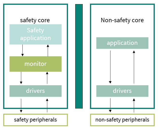
To prevent safety applications with different safety goals interacting with each other, AURIX™ TC3xx devices implement a number of hardware features, allowing them to isolate hardware and software components that are not meant to interfere. A simplified example of “isolation” is represented in
Figure 6
.
In the following sections, an overview of these protection mechanisms is given. It is the user’s responsibility to configure them as per the needs of the safety application.
To ensure the independence between an ASIL function and a QM function, freedom from interference must be achieved in the data, resource and time domains to avoid the following situations:
A hardware/software element corrupts data belonging to another hardware/software element (data domain)
A hardware/software element consumes too much CPU performance or uses a shared resource (internal bus, peripherals, communication network) for a long time, preventing other elements from reaching their execution latency requirements (time domain)
A hardware/software element uses or modifies the configuration of a resource (internal bus, peripheral, communication network) belonging to another application (resource domain)
Figure 6. Example of freedom from interference realization
To ensure freedom from interference from a generic element (hardware or software), it is possible to utilize the AURIX™ TC3xx MCU family features.
Data domain
In the context of embedded systems, the data domain of a specific core can be accessed and shared within the system. It is important to define which parts of the data or memory are exclusively accessible by a particular core (private data) and which parts are shared among multiple cores (shared data). Managing the data domain in embedded systems is crucial for maintaining data consistency, avoiding data conflicts and ensuring efficient inter-core communication.
Memory protection system of the TriCore™ CPU
To implement freedom from interference between software components in the data domain, memory partitioning is generally used. Memory protection in the TriCore™ CPU is facilitated by the robust memory protection system. This safety-relevant feature extends its functionality to both data memory and program memory, offering safeguards against unauthorized read, write or instruction fetch accesses by software running on the CPU.
In the TriCore™ version embedded in the AURIX™ TC3xx MCU (revision 1.6.2), there are six available memory protection register sets. The PSW.PRS bit field (in the range 0-5) determines which of these sets is currently in use by the CPU, as depicted in
Figure 7
.
The CPU's memory protection system operates as a hardware mechanism, providing range-based protection for program memory and data memory. Each protection range is a contiguous part of the address space, precisely defined by lower and upper boundaries, wherein access permissions are specified.
The protection sets are used, in turn, to determine data access and instruction-fetch permissions. The hardware efficiently manages the changing of protection sets during task context switches, ensuring seamless protection and allocation of code execution ranges as well as data ranges. This comprehensive approach guarantees the integrity of the embedded system's memory architecture.
The memory protection is disabled after a reset and no protection ranges are defined. The application must initialize the protection ranges and permissions, adapting them to the software architecture. A few safety operating systems enable this protection immediately after the startup phase.
Several data and code ranges (represented by the blocks called “data regions” and “code regions” in
Figure 7
) can be defined based on the upper and lower boundary registers of each region. Once those regions are set up, a register set (DPRE, DPWE and CPXE) can be associated with some of the available regions by setting the bits corresponding to the read permission enabled data, write permission enabled data and execute permission enabled code for that specific memory region.
Note: More details are in the TriCore™ TC1.6.2 core architecture manual, vol.1, Section 10.
Figure 7. CPU memory protection system usage
Bus memory protection
Each CPU’s memory is also accessible to all bus masters, such as CPUs and DMA. To avoid interference from other bus masters, each shared memory implements a region access protection mechanism. The mechanism, identified as bus memory protection of the CPU, is a hardware mechanism that protects user-specified memory ranges of the CPU's local memories (DSPR, PSPR, DLMU and NVM) from unauthorized write accesses through the SRI slave interface. To implement this mechanism, the system integrator must define the upper and lower boundaries (RGNUA and RGNLA) of a few regions to which some masters can access and others cannot (RGNACCENA and RGNACCENB).
Figure 8. Bus memory protection usage
Using this method, the system integrator can restrict, for example, write access from CPU0 to CPU1 DSPR to a dedicated memory region of DSPR used as a communication buffer between the two cores. Similarly, this mechanism can restrict write access from DMA channels.
For each memory range, one or more masters can be authorized. This mechanism supports the following complex bus memory protection schemes:
Only specifically identified software (safe software) is allowed to write to a region
Only specifically identified DMA channels are allowed to write to a region
Bus memory protection initialization: After reset, the bus memory protection allows access to the entire addressable space for all masters. The application must initialize the protection ranges and permissions adapted to the software architecture. A few safety operating systems enable this protection immediately after the startup phase.
Note: More details are in the TriCore™ TC1.6.2 core architecture manual, vol.1, Section 10.
Time domain
The AURIX™ TC3xx MCU provides a set of hardware functions that enable the application to verify that the static timing properties of the safety-related tasks are met during run-time. Two ways of accomplishing the time monitoring function are available:
Watchdogs
To support time monitoring, MCU provides internal watchdogs. There is one internal watchdog per CPU plus one safety watchdog for the entire MCU
Temporal protection system
The TriCore™ also implements a temporal protection system to guard against run-time overruns. The system consists of two primary mechanisms:
Temporal protection timers
Exception timers
The temporal protection timer system consists of three independent decrementing 32-bit counters, arranged to generate a temporal asynchronous exception (TAE) trap on decrement to zero. On the other side, the exception timer system provides a method of detecting the overrun of exception handlers in the system.
Note: More details are in the TriCore™ TC1.6.2 core architecture manual, vol.1, Section 11.
Resource domain
To control access to their resources and provide freedom from interference in the resource domain, AURIX™ TC3xx modules implement various useful features.
Figure 9. Protection of peripheral resources
Register access protection (AP)
Each on-chip resource with direct or indirect bus master capability has a unique master TAG ID that can be used to identify the master of an on-chip bus transaction. TAG_ID-based protection means that on-chip bus write access to the control registers can be disabled for each master TAG_ID individually. For a disabled master TAG_ID, write access will be disconnected with an error acknowledgement. However, read access will be processed.
This identifier allows each bus slave to select which master is allowed to access its resources. For example, a QSPI peripheral block can be configured in such a way that CPU1 (the master) has no access to its registers. Access to the registers of a functional block (slave) of the MCU is limited by their ACCEN registers, which will set the TAG ID for the masters to which they will be granted the possibility to modify the block registers.
In addition, the access enable registers (ACCEN1/0) are “Safe Endinit” protected. After reset, all ACCEN1/0 access enable bits and access control bits are enabled and access protection mechanisms must be configured and checked to bring the system to a safe state.
TriCore™ privilege levels
The TriCore™ privilege levels control access to peripheral devices and special function registers. Each CPU task or DMA channel is allocated a privilege level, which can be:
User-0 mode
No peripheral access. Access to memory regions with the peripheral space attribute is prohibited and results in a trap. This access level is given to tasks that do not directly access peripheral devices. Tasks at this level do not have permission to enable or disable interrupts
User-1 mode
Regular peripheral access enables access to common peripheral devices that are not specially protected, including read/write access to serial I/O ports, read access to timers and access to most I/O status registers. Tasks at this level may disable interrupts
Supervisor mode
Enables access to all peripheral devices. It enables read/write access to core registers and protected peripheral devices. Tasks at this level may disable interrupts
This feature gives the possibility that only masters with supervisor mode access (in write mode) critical resources, since write accesses to protected registers performed by masters configured in user mode will result in activating alarms to the SMU.
CPU Endinit protection
There are several registers in the TC3xx that are usually programmed only once during the initialization sequence of the system or application. Modification of such registers during a normal application run can have a severe impact on the overall operation of modules or the entire system. While the supervisor mode and the access protection scheme provide a certain level of protection against unintentional modifications, they may not be sufficient to protect against all unintended accesses to system-critical registers.
The AURIX™ TC3xx provides one more level of protection for such registers via the various Endinit features. This is a highly secure write-protection scheme that makes unintentional modifications of registers protected by this feature impossible. Writes are only enabled if the corresponding ENDINIT bit is 0 and supervisor mode is active. Write attempts if this condition is not true will be discarded and the register contents will not be modified in this case. The bus control unit (BCU) controls the operation following a discarded write access and triggers an alarm to SMU.
In addition, each WDT monitors ENDINIT bit modifications by starting a time-out sequence each time software opens access to the critical registers through clearing the corresponding ENDINIT bit. If the time-out period ends before the corresponding ENDINIT bit is set again, a malfunction of the software is assumed and a watchdog fault response is generated. A user-defined password is needed to de-activate the ENDINIT protection and then access critical registers.
Note: Every CPU has its own ENDINIT mechanism, which also means a dedicated watchdog.
Safety Endinit protection
Similarly to the CPU Endinit functionality, which is handled by the CPU watchdogs, the safety watchdog also allows to protect a set of safety-related registers via a safety Endinit locking scheme.
Note: More details about Endinit functions can be found in AURIX™ TC3xx User’s Manual v2.0, vol. 1.
In summary, both Endinit and safety Endinit are mechanisms that contribute to the overall robustness and security of the AURIX™ TC3xx MCU. They help to prevent accidental or malicious alterations to critical settings, ensuring stable and secure operation, with safety Endinit providing an even higher level of protection suitable for safety-critical applications.
Alarm test mechanism
Motivation for this section is that the existing alarm test mechanisms are often challenging to use, and not every hardware mechanism has a corresponding alarm test mechanism.
Many customers test alarms to verify the application’s reaction during development.
To accomplish that, it is possible to simply leave the SMU in START state, and verify each alarm reaction by invoking each alarm with a write to SMU_AGx.
It is important to understand that latent random faults in digital blocks within AURIX™ TC3xx logic are mainly addressed by the LBIST and other runtime safety mechanisms and do not require additional alarm tests.
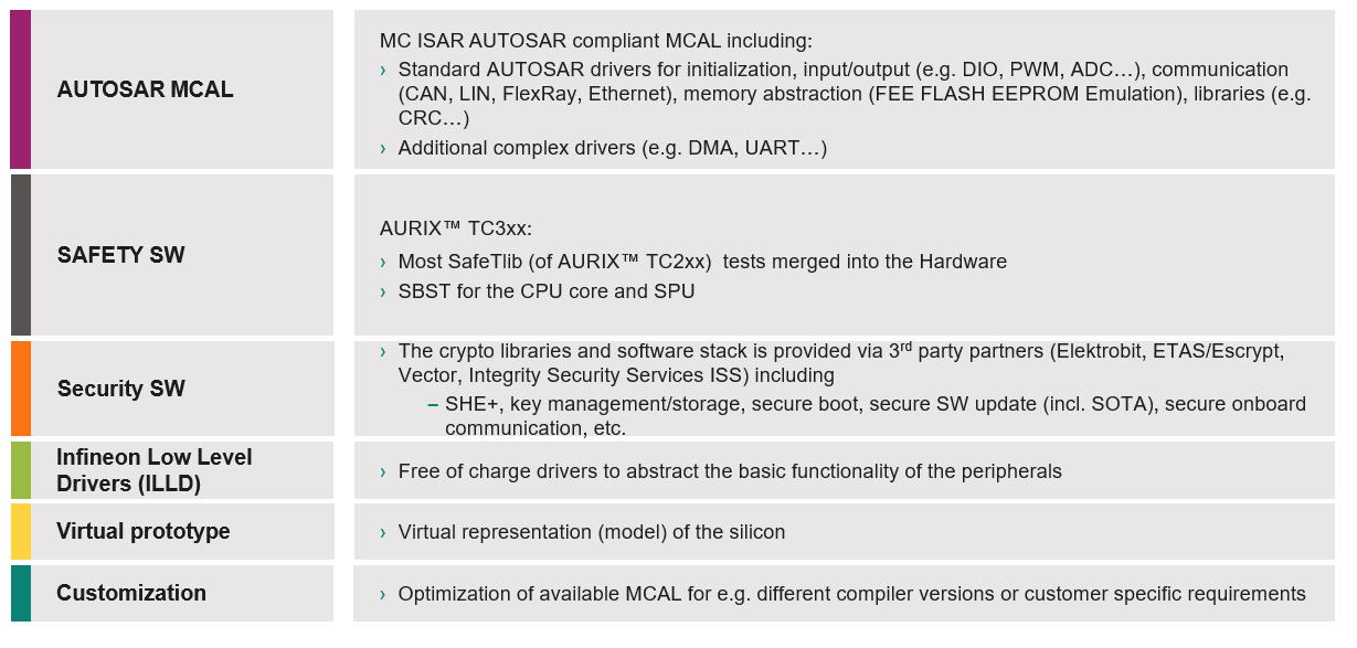
Available AURIX™ TC3xx software
The software development can be done fully in-house or partially using software libraries offered by Infineon or Infineon partners.
shows a brief overview of what Infineon or its partners offer today.
Figure 10. Example of embedded software offered by Infineon or its partners
References
Infineon Technologies AG:
AURIX™ TC3xx User’s Manual
; 81726 Munich; 2021-02; Available online
Infineon Technologies AG:
TriCore™ TC1.6.2 core architecture manual
; Available online
Infineon Technologies AG:
AN1000 - FuSa in a Nutshell - release note
; Available online
Glossary
Definition | Description | Notes |
|---|---|---|
ASC | Active Short Circuit | in the Inverter Use Case |
Architectural Element | The smallest element on which the FMEDA is performed | |
ASIL | Automotive Safety Integrity Level; refer to ISO 26262-1:2018, 3.6 | |
BEV | Battery-powered Electric Vehicle | |
CCF | Common-Cause Failure; refer to ISO 26262-1:2018, 3.18 | |
DC | Diagnostic Coverage; refer to ISO 26262-1:2018, 3.33 | |
DFA | Dependent Failure Analysis identifies single events that can cause multiple sub-parts to malfunction (for example, intended function and its safety mechanism) and lead to a violation of a safety requirement or safety goal. | |
DMI | Data Memory Interface | |
DPF | Dual-Point Failure; for the definition refer to ISO 26262-1:2018, clause 3.38 | |
DSPR | Data Scratch Pad RAM | |
ECU | Electronic Control Unit | |
FHTI | Fault Handling Time Interval is defined in ISO 26262 as the sum of three elements: The fault detection time, the fault reaction time and the time for the system to reach a safe state. | |
FTTI | Fault Tolerant Time Interval; for the definition refer to ISO 26262-1:2018, clause 3.61 | |
FMEA | Failure Mode and Effects Analysis | |
FMEDA | Failure Modes, Effects and Diagnostic Analysis Analysis of the effect of random hardware faults on a safety requirement or safety goal, including quantitative estimation of failure rates and the probability/rate of a safety goal violation | Quantitative Bottom-up HW only |
FTA | Fault Tree Analysis Analysis in which a top-level failure mode is broken down to a combination of lower-level faults (root causes) using a Boolean logic approach | Qualitative (may be quantitative) Top-down HW only |
HARA | Hazard Analysis and Risk Assessment; Refer to ISO 26262-1:2018, 3.76 | |
HW | Hardware | |
IC | Integrated Circuit | |
IEC | International Electrotechnical Commission | |
ISO | International Organization for Standardization | |
LBIST | Logic Built-in Self Test | |
LMU | Local Bus Memory Unit | |
MCU | Microcontroller unit | |
MMIC | Monolithic Microwave Integrated Circuit is a type of integrated circuit (IC) device that operates at microwave frequencies (300 MHz to 300 GHz). These devices typically perform functions such as microwave mixing, power amplification, low-noise amplification and high-frequency switching. | |
PMI | Program Memory Interface | |
PMIC | Power Management ICs (PMICs) | |
PMSM | Permanent Magnet Synchronous Machine (with rare earth material) | Motor type |
PSPR | Program Scratch Pad RAM | |
Safety Flip Flops (SFF’s) | Safety flip-flops are special flip-flops that implement a hardware mechanism capable of detecting bit flips within the protected registers, thus preventing single-point faults. | |
Safety Measure | Activity or technical solution to prevent, detect, control or mitigate systematic and random failures. | |
SBC | system basis chips (SBC) SBCs combine mainly three functionalities in a single device: Power supply, CAN and/or LIN transceivers and supporting features (MCU supervision, SPI interface and so on). This integration makes SBC a potentially better alternative to standalone (discrete) solutions, especially in terms of total solution cost and total area. | |
SE | Soft Error | |
SM | Safety Mechanism: for the definition refer to ISO 26262-1:2018, 3.142 | |
SW | Software | |
SPU | Signal Processing Unit | |
STP | Shoot-Through Protection: Protection typical of an inverter gate driver so that the high side and the low side of the three-phase motor legs cannot be activated simultaneously | |
VCU | Vehicle Control Unit |
Revision history
Document revision | Date | Description of changes |
|---|---|---|
V1.0 | 2024-09-12 | Initial release |
V1.1 | 2025-01-28 | Added section Handling of device unavailability Corrected numbering in clause From B to C - application startup software |
V1.2 | 2025-05-27 | Template updated; no content update |