AP32488 PCB and High Speed Serial Interface (HSSI) design guidelines
32-bit TriCore™ AURIX™ Family
About this document
Scope and purpose
This document provides information for designing High Speed Serial Interfaces (HSSI) on the AURIX™ family of 32-bit microcontrollers from Infineon, covering the TC3x devices. The topics covered include PCB Design considerations regarding the routing of high speed signals, selecting stack-up of the PCB, impedance controlled design of the traces, and termination of high speed signal paths.
For the layout proposals on escape routing and placement of decoupling capacitors please refer to the dedicated PCB design guideline documents of each available package type of the AURIX™ microcontroller family, such as TQFP and LFBGA Packages.
The document should be read in conjunction with Application Note “AN24026 - General Design Guideline for Microcontroller” (available from www.infineon.com).
Intended audience
This document is intended for anyone who designs with AURIX™ microcontroller and needs design recommendations regarding to the EMC optimized PCB and high speed design.
High Speed Board Design
The biggest challenges in high speed design are to minimize the crosstalk and achieve good signal integrity for the transmitted signal, and also to minimize the noise effects on the board. This must be guaranteed for both single ended and differential pair signaling (LVDS) signals, as these are typical high speed interface signal types.
Most of the recommendations are rules that help to avoid the problems but the design process itself must be treated as a trade-off process between the design guidelines. The designer must decide on parameters which have an effect on the performance, reliability and cost of the design.
With those considerations in mind, the following topics should be treated as critical in the design process:
- Selection of stack-up for high speed board design
- Component placement of signal transmitter and receiver circuits
- Impedance controlled design of traces
- Routing of high speed serial signals
- Correct termination of the transmission lines
- Minimizing crosstalk between the signal channels
- Board Level Filtering and Decoupling
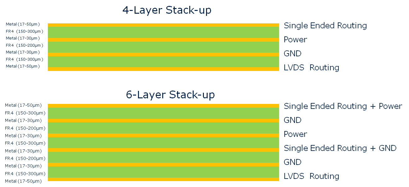
Selection of stack-up for High Speed Board Design
Selection of the correct stack-up for a high speed board should be done at the beginning of the board design because the selection can have an effect on the routing and impedance control of the traces. Impedance control of the traces is one of the main parameters of the high speed design.
The following issues must be considered:
- How can it be guaranteed that high speed lines have a solid GND reference without interruption of the impedance continuity?
- Signal lines must have minimum distance to reference the plane layer.
- Ensure, as much as possible, a plane capacitance for the supply domains.
- How to avoid vias or layer change on high speed signals.
Since the discrete board decoupling capacitors can only be effective up to 200 MHz, the plane decoupling should be used where possible.
The stack-up should be selected so that you can build a power plane capacitance and have the benefit of the high frequency decoupling effect which could be effective above 200 MHz.
The following are sample stack-up of 4-Layer and 6-Layer boards.
Component Placement
- Place the µC and Connector with high speed signals first, to ensure minimal length of the traces
- Do not place other components between these Connectors and the µC
- Place possible noise sources away from the high speed signals
- Components that communicate with devices outside the board should be placed at the edge of the board
Recommendation for unused pins
In case of not using all I/O-Pins of the microcontroller, it is recommended to take some measures on software and PCB. Table-1 gives an overview of the measures for different I/O-Pins. The measures given in the table are optimized from EMC point of view. If this is not required, other measures are also applicable.
| I/O Type | Measure | Reason |
|---|---|---|
Supply Pins (Modules) | See the User´s Manual. | - |
I/O-Pins | Option 1: static low output in weakest driver mode in order to improve EMI behaviour. Option 2: input with pull-up or pull-down. Option 3: input without pull-up or pull-down and disabled input stage using PDISC function. | Leave solder pad open and do not connect it to any other net (layout isolated PCB-pad only for soldering). Ensure by PCB design that the electromagnetic field strength in 6.7 mm distance to the microcontroller does not exceed 800 V/m. Ensure by PCB design that the coupling capacitance from any noisy net to the unused pin is less than 1 pF. |
Output Pins including LVDS | Option 1: static low output in weakest driver mode in order to improve EMI behaviour. Option 2: disable the output driver if static output level is not possible. | Leave solder pad open and do not connect it to any other net (layout isolated PCB-pad only for soldering). Ensure by PCB design that the electromagnetic field strength in 6.7 mm distance to the microcontroller does not exceed 800 V/m. Ensure by PCB design that the coupling capacitance from any noisy net to the unused pin is less than 1 pF. |
Input Pins without internal pull device | Option 1: Connect the pin with a resistor to GND (range 10k – 1Meg). Option 2: Connect a group of up to 8 unused input pins with a resistor to GND (consider the leakage current in order to calculate the resistor value). Option 3: Connect the pin directly to GND. In this case, ensure for DS-ADC analog pins that the analog channel is not connected internally to a reference voltage by checking the corresponding bits in the VCMx registers. Option 4: Disable the input stage using the PDISC function if available. | Ensure by PCB design that the electromagnetic field strength in 6.7 mm distance to the microcontroller does not exceed 800 V/m. Ensure by PCB design that the coupling capacitance from any noisy net to the unused pin is less than 1 pF. |
Input Pins with internal pull device |
|
|
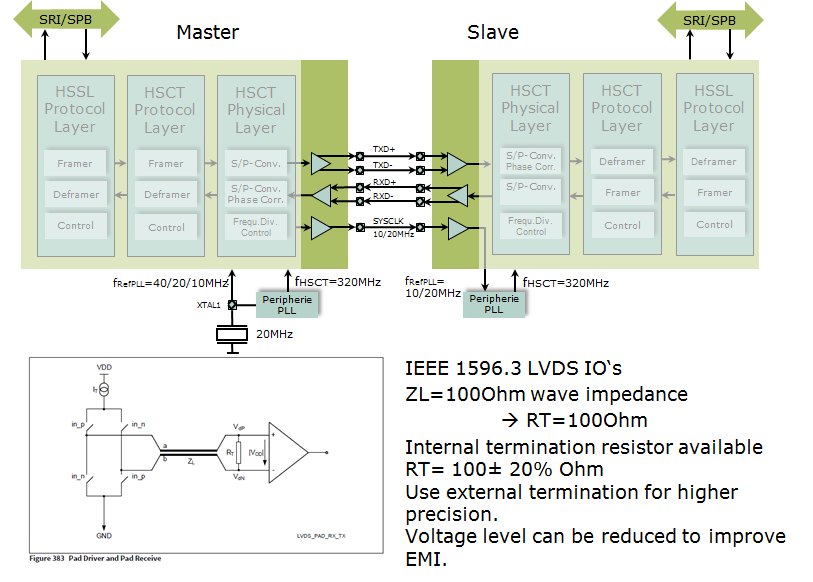
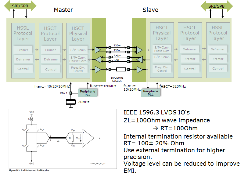
HSCT/HSSL master/slave with separate power supplies
A master and slave may each have their own dedicated power supply. To address the situation in which the slave might have lost it’s own power supply (temporarily or permanently) but the master supply is still operating, it is necessary to reduce the over-load current which would go from the SYSCLK master (transmit) to the SYSCLK slave (receive).
Over-load reduction can be achieved by using a serial resistor placed close to the receiver input, with far- end termination at the SYSCLK slave. The serial resistor should be as small as possible to avoid degradation of HSCT/HSSL bit-error rate.
The Absolute Maximum ratings for Input current on any pin during an overload condition are +/-10 mA.
The other HSCT/HSSL pins are either in:
LVDS state
- if in active state the LVDS current is limited by LVDS gain control
Passive state
- receive state
The additional delay has no functional disadvantage because the SYSCLK is not synchronized to the bitstream CLK recovery. Only a precise capture CLK is required for CLK recovery. The SYSCLK phase shift is excluded by the HSCT/HSSL PLL phase selection.
Optionally it is possible to implement a periodic or continous slave-supply monitoring. In case of slave supply fail condition, the master SYSCLK must be switched off to avoid the pad overload condition of the unsupplied slave SYSCLK input pad.
Figure 2 Default HSCT/HSSL configuration, with master and slave at the same supply
Figure 3 HSCT/HSSL configuration with dedicated supplies for both master and slave
Impedance Controlled Design of Traces
Design of traces for high speed signals is critical. They should be designed to have a trace impedance of 50 Ohm and differential impedance of 100 for LVDS signals.
There are two types of transmission lines for trace implementation:
- Microstrip
- Stripline
Depending on the selected stack-up for the design, calculate the characteristic impedance for either microstrip or stripline transmission line to have 50 Ohm trace impedance.
Microstrips
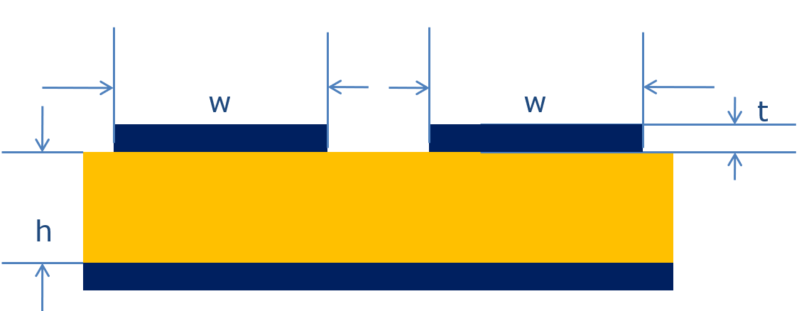
Formula:
(Formula is valid when 0.1<w/h<2.0 and 1<ε<15) [2]
Striplines
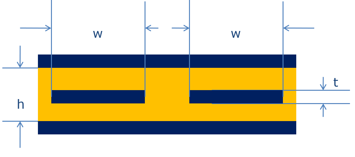
Formula:
(Formula is valid when w/h<0.35 and t/h<0.25) [2]
Key to formulas
- h
- for microstrip = Height over ground
- for stripline = Separation between grounds
- w = trace width
- t = Line Thickness
- εr = Relative Permittivity of substrate (all distance units are Inches)
Transmission line parameter
It is possible to calculate the impedance of the traces by using the transmission line parameter. The parameter can be delivered by the PCB manufacturers.
To determine if the trace has to be considered as controlled impedance trace (critical length), the following rule and calculation can be used:
- If the trace is longer than ¼ of the distance covered by the rise time of the signal, then the controlled impedance should be applied.
Sample calculation (for FR4 material and 500ps rise time):
Propagation velocity:
Distance at rise time:
Critical Length:
From the EMI point of view it is recommended to use striplines, since they are placed on the inner layer where the traces cannot cause radiation to the outside of the board. But striplines require a layer change which can cause impedance discontinuity and this will result in reflections. It is also difficult to meet the impedance requirement of 50 Ohm for trace and 100 Ohm differential impedance because of different reference layers.
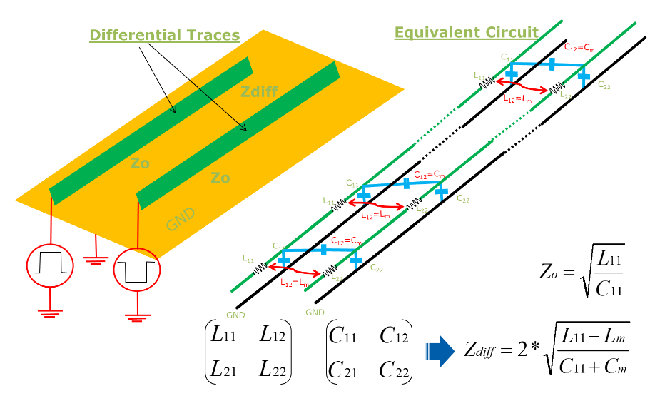
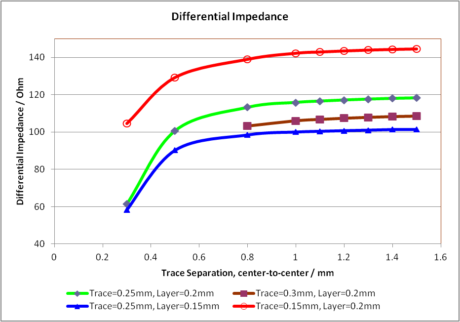
The differential impedance is dependent on:
- the distance between the lines
- the distance to the reference plane
For the correct calculation of the trace and differential impedance, 2D field solvers or the Signal Integrity capability of the layout tool can be used. Most of the tools on the market offer this. In this case it is possible to route the lines without worrying about the impedance calculation, since the tool calculates and adapts the parameter so that impedance controlled lines are always guaranteed.
The following rules must also be applied in the design and routing:
- Use traces that are as wide as possible
- Microstrip lines are recommended as the differential signaling cancels most of the radiation
- In there are still radiation problems, the stripline design can also be used
- Keep trace width/spacing ratio less than 0.8 to reduce the effect on trace impedance
- Ensure that 50 Ohm trace and 100 Ohm differential impedance with a tolerance of ±10% can be guaranteed by the manufacturer of the PCB
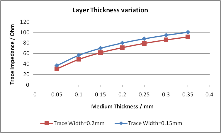
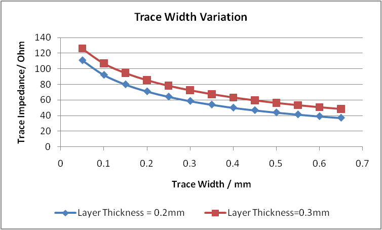
Estimating trace dimensions
The following diagrams (valid for 35 µm thick Microstrips) can be used to estimate the trace dimensions in the early design phase before final impedance calculations are made.
Routing of High Speed Serial Signals
- High speed signals should be routed first to reach the required specification for impedance continuity, across a short distance and with optimal channel design.
- Do not place traces over split planes. Traces should have a solid reference GND plane over the whole length without interruption to avoid impedance discontinuity and reflections.
- Keep in mind that the return current path should be close to the signal line. The current loop should be as small as possible.
- Keep the traces as short as possible.
- Route traces straight. Point-to-point connections are required for differential lines and do not use daisy-chain routing. If required, do not use stubs along the daisy-chain connections.
- Do not used 90° bending instead of 45°, if it cannot be avoided.
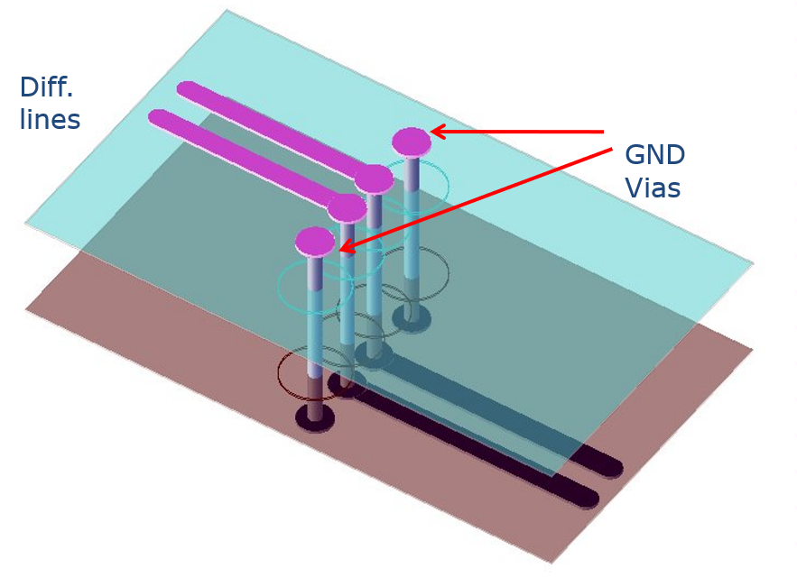
- Do not use layer changes and avoid vias on traces.
- If a layer change is necessary, use a solid GND reference.
- Place GND vias near the signal lines (Differential via – GSSG) if a layer change cannot be avoided
All differential traces must be matched in length.
- Length differences between differential traces can cause skew between the differential lines. Skew has an effect on common mode and reduces the voltage swing.
- Keep the length difference of the differential traces less than 2 mm.
Route single ended traces on different layers to the differential lines, or keep a minimum distance of 4 traces wide to each other, to minimize the crosstalk.
Avoid impedance discontinuity along the trace.
- SMT Pads of AC coupling capacitors which are referenced to GND planes can have different impedance to the required 50 Ohm. In that instance the GND plane underneath the pads can be removed, but it will be necessary to ensure field solver analysis on the resulting impedance.
Correct Termination of Transmission Lines
There are different types of termination techniques:
- Near End (source) Termination
- Far End Termination
Near End (Source) termination
This is normally used by the single ended lines where the output driver has lower impedance than the transmission line. In this case the series termination is added to the output of the driver to match the line impedance.
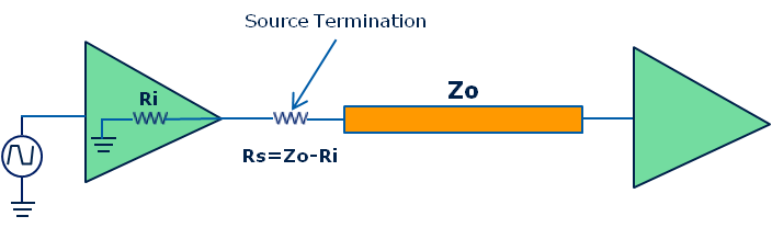
- Place the resistor very close to the source driver.
- Use source termination in cases of point-to-point connection.
- Do not use daisy-chain topology.
- All loads must be at the end of the line.
- Ri Fast/RFast padclass strong driver = typ 55 Ohm
- Ri RFast padclass RGMII driver = typ 20 Ohm
Far End termination
The most common type of Far End termination for HSSI is Parallel or AC Termination.
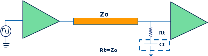
- Parallel termination resistance should be matched to the characteristic impedance of the line.
- Parallel termination causes power consumption due to the DC path at the end of the line for high signal level. The thermal treatment should be done by selection of the parallel termination resistor.
- The power consumption can be avoided with AC termination, where a capacitor is inserted in series to the termination resistor.
- The Capacitor value in AC termination should be in the range of 100-200 pF.
- This termination technique increases the rising and falling times at load due to the capacitive load. Timing considerations should be made by selection of the value of C.
- Place the components close to the receiver pins so that no long stubs are required.
Termination of Differential lines
Special attention should be given to the termination of the differential lines.
The differential lines require more than 50 Ohm line impedance and 100 Ohm differential impedance between the lines. So the termination must be matched to the 100 Ohm.
- Place termination after the connection of the trace to the pin of receiver so that no stubs are created before the receiver. This avoids reflections generated by the impedance discontinuity.
- Do not use layer change or a via for the placement of the termination.
Minimizing Crosstalk between Signal Channels
Coupling of the electrical signals occurs if lines are routed parallel for a long distance.
Coupling problems can be avoided with careful PCB design:
- Separate the routing layer for single ended and differential signals.
- Route all traces perpendicular if two adjacent layers have high speed lines.
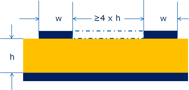
- Do not route signals closer than 4 times the electrical height to the reference.
- Reduce the distance to the reference layer as much as possible.
- A transmission line which has lower distance to the reference plane has less coupling to the adjacent traces.
- Avoid parallel routing of high speed signals over long distances.
- For the differential signals, keep the distance constant along the length of the traces.
- If serpentine routing (to match the differential length of traces) is required, separate the parallel running traces 4 times the dielectric height.
- Apply serpentine routing for length matching at the transmitter side rather than the receiver side.
- Route critical signals on adjacent layers orthogonal to each other.
Board Level Filtering and Decoupling
Decoupling the Power Distribution Network of the microcontroller IC is critical to the PCB design process, because careful selection of the decoupling capacitors and placement has a big influence on the high speed performance of the board, and can reduce the emissions. The on-board decoupling capacitors have an effective range of 1 MHz – 200 MHz. The range above 200 MHz can be covered by using power plane capacitance.
The effectiveness of the decoupling capacitors depends on the optimum placement and connection type.
Place capacitors as close as possible to the µC.
Keep the interconnection inductance of capacitors to the µC as low as possible.
Use low effective series resistance and inductance (ESR and ESL) capacitors.
- Since parasitic inductance is the limiting factor of the capacitor response to high frequency demand of current from the device, the ESL of the capacitor and the connection inductance should be selected so that the optimum value for the design is reached.
Connect capacitors with vias close to the side of the pads.
- Use side placement of the vias to reduce the current loop.
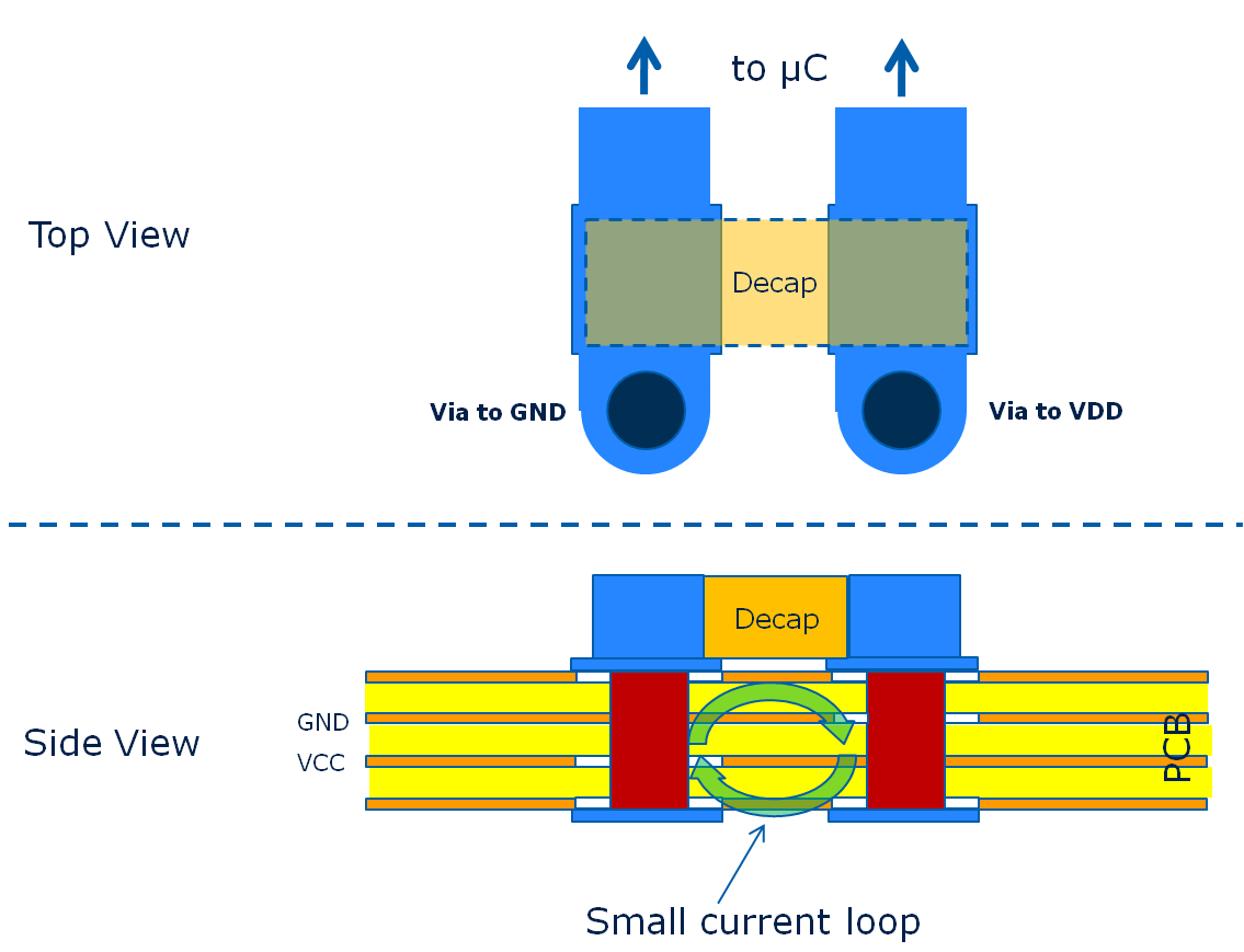
Dual vias can be used to reduce the parasitic inductance.
Solder lands, traces and vias should be optimized for capacitor placement.
Do not use long traces to connect capacitors to GND or to VDD.
- Always keep the return path of the high frequency current (lowest inductance path) small.
Select the smallest package available for the capacitors.
- Select capacitors of type: ceramic multilayer X7R or X5R.
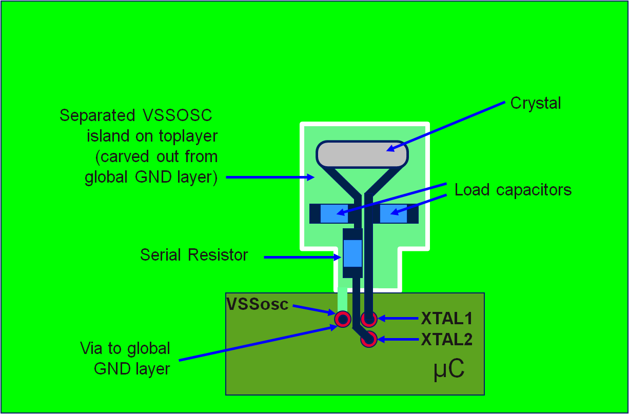
To reduce the radiation / coupling from the oscillator circuit, a separated ground island on the GND layer should be made. This ground island can be connected at one point to the GND layer.
- This helps to keep noise generated by the oscillator circuit locally on this separated island.
- The ground connections of the load capacitors and VSSOSC should also be connected to this island.
- Traces for the load capacitors and Xtal should be as short as possible.
To minimize the EMI radiation on the PCB, the following signals are to be considered as critical:
- Ethernet Pins (RGMII,RMII,MII)
- HSPDM Pins
- SDMMC Pins
- Single ended CLK Pins (SYSCLK, EXTCLK, Module CLKs)
- Single ended Data Pins (MSC, ERAY,SPI)
- LVDS Pins (HSCT, MSC, QSPI, AGBT)
- Supply Pins
- Route these signals with adjacent ground reference and avoid signal and reference layer changes.
- Route them as short as possible.
- Routing ground on each side can help to reduce coupling to other signals.
The ground system must be separated into analog and digital grounds. The analog ground must be separated into two groups:
- Ground for OSC / PLL supply pins (VSS_OSC) as common star point.
- Ground for ADC (VSSM for VDDM) as common star point.
The power distribution from the regulator to each power plane should be made over filters.
RC Filters can be inserted in the supply paths at the global regulator output (global supply star point) and at the branching to other module supply pins like Vflex, Vflex1 and VDDM.
- Using inductance or ferrite beads (5 – 10 µH) instead of the resistors can improve the EME behavior of the circuit and reduce the radiation up to ~10dBµV on the related supply net.
- OCDS must be disabled.
- Select weakest possible driver strengths and slew rates for all I/Os (see Scalable Pads Application Note AP32111).
- Avoid cutting the GND plane by via groups. A solid GND plane must be designed.
HSSI on AURIX products
For general information about microcontroller PCB design guidelines please refer to the Infineon document AP24026 and for Giga-Bit Ethernet interface to the document AP32368.
2.5 Gbit/s HSSI (AGBT)
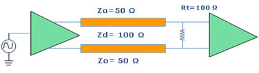
2.5 Gb/s HSSI is an LVDS interface with a maximum voltage drive level of ±400 mV. The routing of the signals should be treated as critical and the designer should give maximum attention to the routing. The 50 Ohm trace impedance and the differential impedance of 100 Ohm are the most important requirements of this interface.
HSSL/HSCT Interface
HSCT Interface is an LVDS interface with a maximum data rate of 320 Mb/s. It requires 50 Ohm trace and 100 Ohm differential impedance. Please refer for the Multi-Drop application of HSSL/HSCT interface to the document AP32412.
DAP Interface
For DAP interface signals, it is recommended to apply the serial termination method on both Ends for the DAP1 signal, since this is a bi-directional line (same for DAP2 if used).
Keep the trace length of DAP1 and DAP2 equal.
The DAP0 signal can be terminated only at source (depending on the capability of the DAP0 driver). The terminations must accordingly match to the line impedance.
It is recommended to use a total trace length less than 10 cm for this interface on the boards (load parasitic of the cable has also to be considered).
The following are important rules for single-ended signal design for the DAP interface:
Do not use multiple signal layers to route the clock signal (DAP0).
Use a reference layer below the signal lines and avoid reference changes.
If possible, place the clock signal between two reference layers (GND // DAP0 // GND).
Route first the clock line DAP0 and use a straight line for connection.
Minimize via count on signal lines (if possible, do not use any).
Keep an appropriate distance between the single-ended lines.
If daisy-chain routing is required, avoid stubs at connection points.
- If stubs cannot be avoided, use optional placement resistors to de-couple the chain to get well defined line impedance.
Design line impedance according to the selected operating driver strength of the DAP interface.
Use a series termination method if necessary and calculate the value of series resistance depending on the selected driver strength.
- For example: For the strongest driver setting (for Fast Type) the output impedance is typically 55R, so the series termination resistance is not needed. For the case that a flat ribbon cable is used (75R), select 20R. For both cases the PCB trace impedances on both sides must be designed accordingly.
References
- Infineon Application Note, AP24026 – EMC and System-ESD Design Guideline for Board Layout
- High Speed Digital Design, A Handbook of Black Magic, H.Johnson and M. Graham
- High-Speed Digital System Design, A Handbook of Interconnect Theory and Design Practices, S.H. Hall, G.W. Hall, J.A. McCall
Xilinx, “Spartan-6 FPGA PCB Design and Pin Planning Guide”, UG393 (v1.2) July 15, 2010
http://www.xilinx.com/support/documentation/user_guides/ug393.pdf
Revision history
| Document revision | Date | Description of changes |
|---|---|---|
V1.0 | 2019-05-08 | Initial version – not released |
V1.1 | 2021-07-06 | Figure 4 removed |
V1.2 | 2024-04-17 | Template update; no content update. |