AP32480 PCB Design Guidelines for LFBGA-180 Package
TriCore™ AURIX™ TC3xx Family
About this document
Scope and purpose
The TC33x, TC35x and TC36x are part of the AURIX™ TC3xx family of 32-bit microcontroller products. They are available in different packages and might require a PCB carefully designed for electromagnetic compatibility.
This document provides product-specific EMC design recommendations and PCB guidelines for the TC33x, TC35x and TC36x in LFBGA-180 package, and should be read in conjunction with the Infineon PCB Design Guidelines for Microcontrollers (AP24026), which gives general design rule information for PCB design.
Attention: This document contains design recommendations from Infineon Technologies point of view. Effectiveness and performance of the final application implementation must be validated by the customer, based on their specific implementation choices.
Intended audience
This document is intended for anyone who designs with AURIX™ TC3xx microcontroller and needs design recommendations regarding to the EMC optimized PCB design.
General Information
The microcontroller has following supply domains which should be decoupled individually:
-
VDD/VDDOUT=1.25V for Core / Oscillator/ PLL/ Flash Sense Amp.
-
VDDP3=3.3V for Flash charge pumps.
-
VEXT=3.3V/5V
-
VFLEX=3.3V/5V
-
VEVRSB =3.3V/5V
-
VDDM=3.3V/5V for ADC
The power supply feeding from the regulator outputs to each domain can be made on a supply layer (POWER).
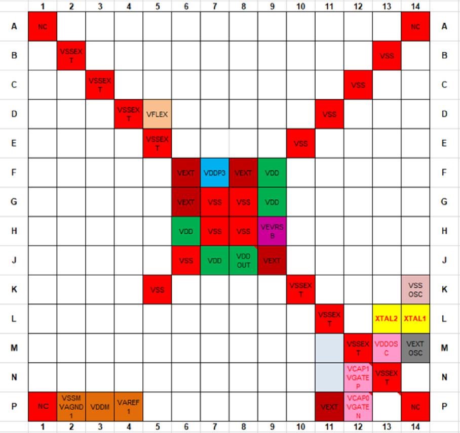
Pinout
Figure 1. LFBGA-180 Pinout
PCB Design
This chapter introduces some ground rules for EMC-friendly PCB layout. More information is provided in the Infineon PCB Design Guidelines for Microcontrollers (AP24026). This document is recommended as an additional information source.
Decoupling the Power Distribution Network of the microcontroller IC is critical to the PCB design process, because careful selection of the decoupling capacitors and placement has a big influence on the high speed performance of the board, and can reduce the emissions.
The on-board decoupling capacitors have an effective range of 1 MHz – 200 MHz.
The range above 200 MHz can be covered by using power plane capacitance.
The effectiveness of the decoupling capacitors depends on the optimum placement and connection type.
General Recommendations
-
Place the µC and Connector with high speed signals first, to ensure minimal length of the traces.
-
Place possible noise sources away from the high speed signals.
-
Components that communicate with devices outside the board should be placed at the edge of the board. (depending on application)
-
Place decoupling and buffer capacitors as close as possible to the µC.
-
Keep the interconnection inductance of capacitors to the µC as low as possible.
-
Use low effective series resistance and inductance (ESR and ESL) capacitors.
-
Since parasitic inductance is the limiting factor of the capacitor response to high frequency demand of current from the device, the ESL of the capacitor and the connection inductance should be selected so that the optimum value for the design is reached.
-
Connect capacitors with vias close to the side of the pads.
-
Use side placement of the vias to reduce the current loop.
-
Dual vias can be used to reduce the parasitic inductance.
-
Solder lands, traces and vias should be optimized for capacitor placement.
-
Do not use long traces to connect capacitors to GND or to VDD.
-
Always keep the return path of the high frequency current (lowest inductance path) small.
-
Select the smallest package available for the capacitors.
-
Select capacitors of type: ceramic multilayer capable of high temperature (example X7R).
-
To minimize the EMI radiation on the PCB, the following signals are to be considered as critical:
- ERAY Pins
- DAP
- Ethernet Pins
- MSC Pins
- QSPI Pins
- External Clock Pins
- SYSCLK
- Supply Pins
− Route these signals with adjacent ground reference and avoid signal and reference layer changes.
− Route them as short as possible.
− Routing ground on each side can help to reduce coupling to other signals.
− OCDS must be disabled.
− Select weakest possible driver strengths and slew rates for all I/Os.
− Avoid cutting the GND plane by via groups. A solid GND plane must be designed.
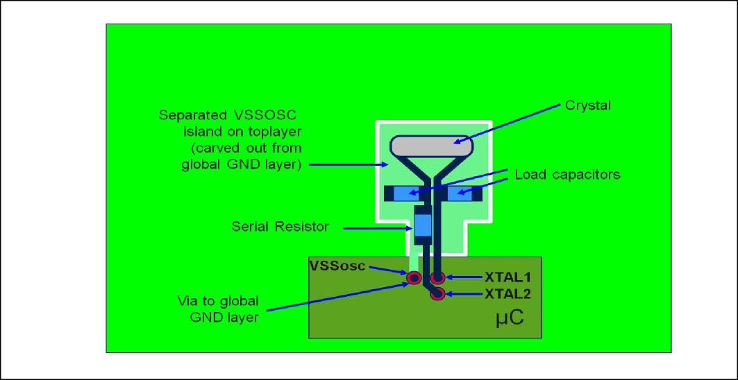
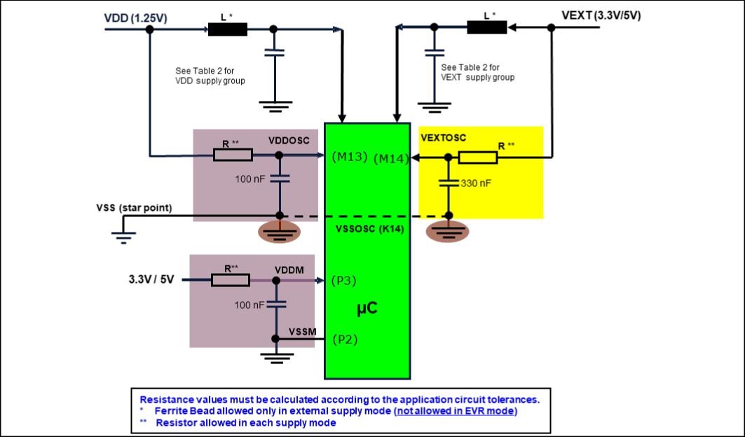
Oscillator Circuit PCB Design
To reduce the radiation / coupling from the oscillator circuit, a separated ground island on the GND layer should be made. This ground island can be connected at one point to the GND layer. This helps to keep noise generated by the oscillator circuit locally on this separated island. The ground connections of the load capacitors and VSSOSC should also be connected to this island. Traces for the load capacitors and Xtal should be as short as possible.
Figure 2. Layout proposal for oscillator circuit (shown for BGA package)
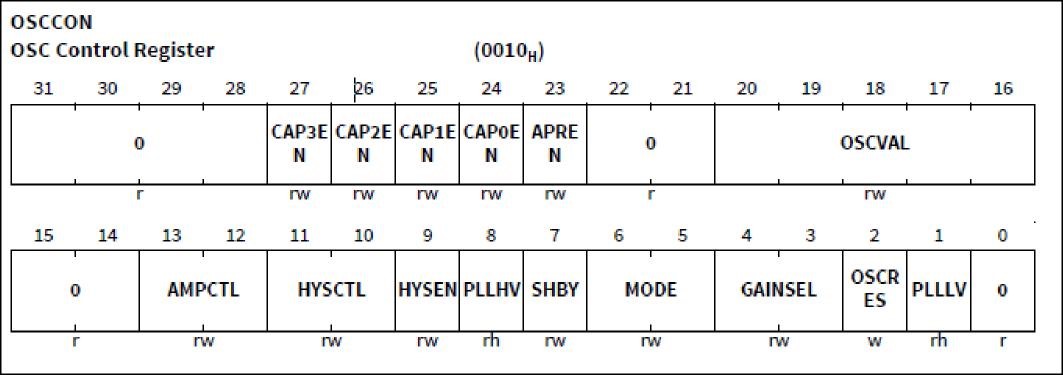
Oscillator Software Setting at external input Clock Mode
To reduce the radiation, coupling, and system jitter from the oscillator circuit for external input Clock mode (where only XTAL1 is externally driven and XTAL2 is open), the CGU OSCCON register must be set to mode 10.
In this External Input Clock mode the oscillator Power-Saving mode is entered. XTAL2 is de-activated.
Figure 3. Osc Control Register
Filtering
-
Ground for OSC / PLL supply pins should be laid out as local island.
-
Analog and digital grounds are connected inside the microcontroller. Therefore the ground for ADC (VSSM for VDDM) should be routed depending on external noise conditions:
- Use common star point in case external noise should be prevented from entering the analog domain.
- Use common ground plane otherwise. (Please refer to the Chapter 6 of the Application note AP32362 “A/D converter Supply and PCB Design Guidelines” for additional details.
-
The power distribution from the regulator to each power plane should be made over filters.
-
RC Filters can be inserted in the supply paths at the regulator output and at the branching to other module supply pins like VDDOSC and VEXTOSC (for osc.), VAREF and VDDM.
-
Using inductance or ferrite beads (5 – 10 μH) instead of the resistors can improve the EME behaviour of the circuit and reduce the radiation up to ~10dBμH on the related supply net.
-
No series resistor beads allowed in the main supply lines.
Figure 4. Filtering of VDDOSC, VEXTOSC and VDDM supply pins
Recommendation for unused pins
In case of not using all I/O-Pins of the microcontroller, it is recommended to take some measures on software and PCB. Table 1 gives an overview of the configuration options for different pin types.
| I/O Type: | Pin configuration | PCB recommendations |
|---|---|---|
Supply Pins (Modules) | See the User´s Manual. | Figure 8 |
I/O-Pins | Option 1: static low output in weakest driver mode in order to improve EMI behaviour. Option 2: input with pull-up or pull-down. Option 3: input without pull-up or pulldown and disabled input stage using PDISC function. | Leave solder pad open and do not connect it to any other net (layout isolated PCB-pad only for soldering). Ensure by PCB design that the electromagnetic field strength in 6.7 mm distance to the microcontroller does not exceed 800 V/m. Ensure by PCB design that the coupling capacitance from any noisy net to the unused pin is less than 1 pF. |
Output Pins including LVDS | Option 1: static low output in weakest driver mode in order to improve EMI behaviour. Option 2: disable the output driver if static output level is not possible. | Leave solder pad open and do not connect it to any other net (layout isolated PCB-pad only for soldering). Ensure by PCB design that the electromagnetic field strength in 6.7 mm distance to the microcontroller does not exceed 800 V/m. Ensure by PCB design that the coupling capacitance from any noisy net to the unused pin is less than 1 pF. |
Input Pins (including analog channels) without internal pull device | Option 1: Connect the pin with a resistor to GND (range 10k – 1Meg). Option 2: Connect a group of up to 8 unused input pins with a resistor to GND (consider the leakage current in order to calculate the resistor value). Option 3: Connect the pin directly to GND. In this case, ensure for DS-ADC analog pins that the analog channel is not connected internally to a reference voltage by checking the corresponding bits in the VCMx registers. Option 4: Disable the input stage using the PDISC function if available. | Ensure by PCB design that the electromagnetic field strength in 6.7 mm distance to the microcontroller does not exceed 800 V/m. Ensure by PCB design that the coupling capacitance from any noisy net to the unused pin is less than 1 pF. |
Input Pins with internal pull device | Option 1: configure the pin as pull-up or pull-down (the User´s Manual may require either low or high level for alternate function). Option 2: input without pull-up or pulldown and disabled input stage using PDISC function. | Leave solder pad open and do not connect it to any other net (layout isolated PCBpad only for soldering). Ensure by PCB design that the electromagnetic field strength in 6.7 mm distance to the microcontroller does not exceed 800 V/m. Ensure by PCB design that the coupling capacitance from any noisy net to the unused pin is less than 1 pF. |
HSCT/HSSL master/slave with separate power supplies
A master and slave may each have their own dedicated power supply. To address the situation in which the slave might have lost it’s own power supply (temporarily or permanently) but the master supply is still operating, it is necessary to reduce the over-load current which would go from the SYSCLK master (transmit) to the SYSCLK slave (receive).
Over-load reduction can be achieved by using a serial resistor placed close to the receiver input, with far- end termination at the SYSCLK slave. The serial resistor should be as small as possible to avoid degradation of HSCT/HSSL bit-error rate.
The Absolute Maximum ratings for Input current on any pin during an overload condition are +/-10mA.
The other HSCT/HSSL pins are either in:
-
LVDS state
- if in active state the LVDS current is limited by LVDS gain control
-
Passive state
- receive state
The additional delay has no functional disadvantage because the SYSCLK is not synchronized to the bitstream CLK recovery. Only a precise capture CLK is required for CLK recovery. The SYSCLK phase shift is excluded by the HSCT/HSSL PLL phase selection.
Optionally it is possible to implement a periodic or continous slave-supply monitoring. In case of slave supply fail condition, the master SYSCLK must be switched off to avoid the pad overload condition of the unsupplied slave SYSCLK input pad.
Figure 5. Default HSCT/HSSL configuration, with master and slave at the same supply
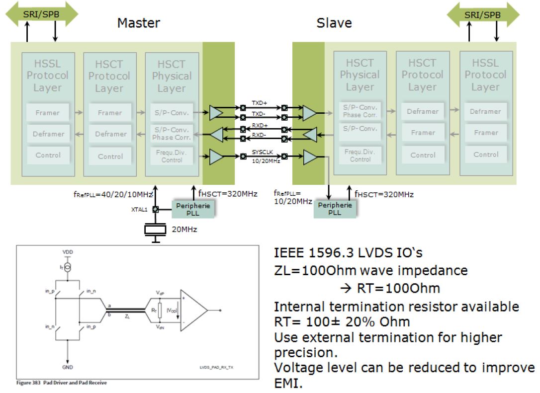
Figure 6. HSCT/HSSL configuration with dedicated supplies for both master and slave, with a serial resistor far-end termination at slave SYSCLK input for over-load current reduction
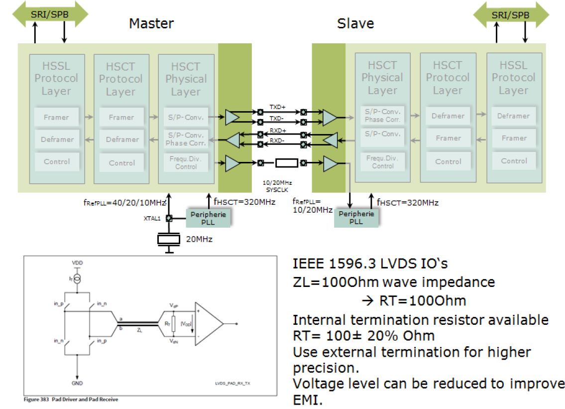
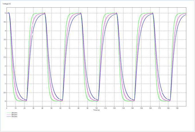
Figure 7. Simulation results (using IBIS model) for HSCT/HSSL configuration with dedicated supplies for both master and slave, with 500 Ohm resistor far-end termination at slave SYSCLK input for over-load current reduction. Slopes for recommended case 500 Ohm for VEXT 5V supply.
Example Layouts for the AURIX TC3xx family
The AURIX™ TC33x, TC35x, and TC36x 32-bit microcontroller products are available in the following packages:
-
TQFP-80
-
TQFP-100
-
TQFP-144
-
LQFP-144
-
LQFP-176
-
LFBGA-180
-
LFBGA-292
Below is an example layout and recommended capacitor list given for the BGA-180 type package of the AURIX™ TC3xx family. Planes are recommended for digital supplies. For analog supplies, no planes are recommended; no noisy traces should be routed through the “Analog areas” marked in the pictures below.
The microcontrollers have the following supply domains:
-
VDD/VDDOUT=1.25V for Core / Oscillator/ PLL/ Flash Sense Amp.
-
VDDP3=3.3V for Flash charge pumps.
-
VEXT=3.3V/5V
-
VFLEX=3.3V/5V
-
VEVRSB =3.3V/5V
-
VDDM=3.3V/5V for ADC
The power supply feeding from the regulator outputs to each domain can be made on a supply layer (POWER).
Example Layout for LFBGA-180 Package
Figure 8. Example layout for LFBGA-180 Package
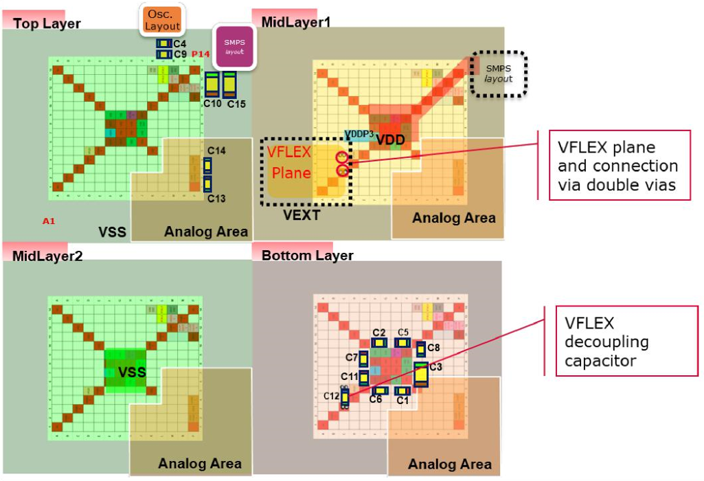
| Capacitor | Value | Supply | LFBGA-180 Pin |
|---|---|---|---|
C1, C2 | 2 x 100 nF | VDD | H6//J7, F9//G9 |
C3 | 1 x 100 nF | VDD VDDOUT (for TC336PD/ED) | J8 |
C4 | 1 x 330 nF | VDDOSC//VSSOSC | M13//K14 |
C5 | 1 x 100 nF | VEVRSB | H9 |
C6, C7, C8 | 3 x 100 nF | VEXT | F6//G6, F8, J9 |
C9 | 1 x 330 nF | VEXTOSC//VSSOSC | M14//K14 |
C10 | 1 x 100 nF for external supply mode 1 x 4.7 µF for SC DC-DC for TC336ED-PD 1 x 10 µF for Coil DC-DC for TC356/TC366 | VEXT//VSSEXT | P11//N13 |
C11 | 1 x 100 nF for external supply mode 1 x 2.2 µF for LDO mode | VDDP3 | F7 |
C12 | 1 x 100 nF for ETH-MII / RMII mode 2 x 100 nF for ETH-RGMII | VFLEX //VSSEXT | D5//D4 |
C13 | 1 x 100 nF | VDDM//VSSM | P3//P2 |
C14 | 1 x 100 nF | VAREF1//VSSM | P4//P2 |
C15 | 1 x 1 µF for TC336ED-PD | VCAP1//VCAP0 | N12//P12 |
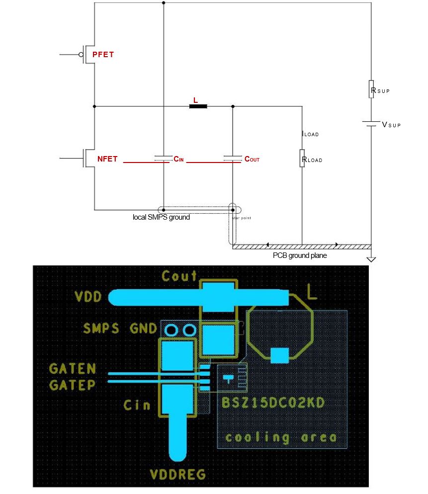
Example Layout for SMPS/DC-DC regulator
Figure below shows an example layout for SMPS EVRC regulator of the core domain. SMPS components below represent one of the usecases. Please refer to the application note AP32344 “TC3xx SMPS regulator” for additional details on component selection, schematic and layout considerations in various usecases of the core domain voltage generation. These usecases take into account conditions such as core domain current consumption, SMPS switching frequency and input voltage range. For each of these combinations component recommendations are given in the Chapter 1.2 of the appnote above as well as the PCB aspects of the SMPS regulator in the Chapter 3.
Figure 9. Example schematics and layout of SMPS/DC-DC regulator (Core current Idd <1.5A, switching frequency 1.8 MHz, Vext = 3.3V/5.0V)