AP32467 DMA linked list modes
32-bit AURIX™ microcontrollers
About this document
Scope and purpose
The Direct Memory Access (DMA) module in the Infineon AURIX™ microcontroller family supports linked list modes. Compared to setting up a normal DMA transaction a DMA linked list can be slightly more complex to program and so this document aims to provide some guidance. We provide an overview of the DMA linked list modes in the TC3xx AURIX™ microcontrollers and provide some programming examples.
Intended audience
This document is intended for software programmers who are already familiar with programming the DMA module in the AURIX™ microcontroller, and wish to make use of the DMA linked list mode. Note:
The example code follows Tasking compiler syntax where relevant.
DMA transactions basics
The DMA is used to perform data transfers without CPU intervention. For example the DMA can transfer data from Memory to Memory, or Memory to Peripheral, or vice-versa. In the DMA there are multiple channels (128 channels in TC39x for example) which can be independently programmed to perform different data transfers. Such data transfers can be broken down into a sequence of reads and writes on the buses (SRI, SPB) in the AURIX™ microcontroller.
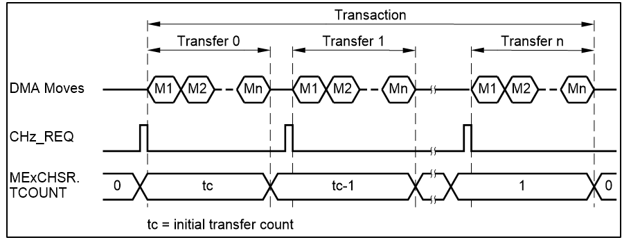
One such read and write operation is known as a DMA Move. A set of such moves constitute a DMA Transfer.
The DMA in the AURIX™ microcontroller is programmed to perform DMA Transactions. Each DMA Transaction consists of a set of DMA transfers, which in turn consists of a certain number of DMA moves. Figure 1 explains this relationship between DMA Moves, Transfers and Transactions.
Figure 1. DMA Moves, Transfers and Transactions
Depending on the configuration of the RROAT field of the CHCFGRz register, DMA transfers may be requested by a software or a hardware trigger.
DMA hardware requests are triggered by specific request lines from the Interrupt Router (IR) or from other DMA channels. Typically the parallel occurrence of DMA requests and interrupts requests for DMA channels is possible.
The DMA controller primarily consists of DMA channels, sub-blocks (Move Engines) and a bus switch. Once configured, the DMA sub-blocks are able to act as a master on the SPB Bus and on the SRI Bus, and execute the DMA Transactions programmed in various DMA channels.
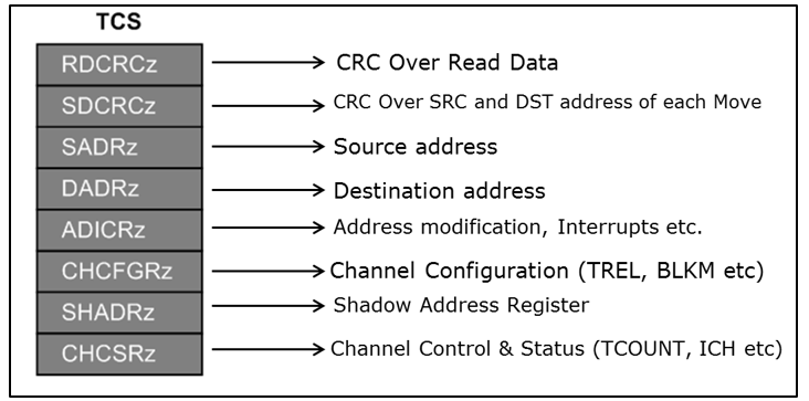
Transaction Control Set (TCS)
In order to program a DMA transaction in a DMA channel, a set of 8 x 32-bit registers have to be configured for the channel. This set of 8 registers is known as the Transaction Control Set (TCS). One such set of registers exist for each implemented DMA channel in the device.
Figure 2 shows the 8 registers in a channel’s transaction control set.
Figure 2. DMA Transaction Control Set
If you do not know how to program a basic DMA transaction, please refer to the user manual and iLLD examples. In this document we will focus only on how to program the various DMA linked list modes.
DMA linked list modes
Linked lists are an extension of the DMA channel functionality which executes a single transaction. Linked lists consist of a series of DMA transactions executed by the same DMA channel z. Each DMA transaction has a unique Transaction Control Set (TCS). The source and destination areas do not have to exist in contiguous areas of memory. The new DMA transaction can issue a DMA software request and auto-start the DMA transaction bypassing the Interrupt Router and so reducing the cumulative latency over a number of DMA transactions.
Linked list advantages
The advantages of using a linked list to perform a series of different DMA transactions are:
-
There is no reprogramming required at the end of each DMA transaction. If the DMA transactions are executed independently, the software would have to reprogram the channel at the end of each one, for the next. This reduces overall CPU load and may improve the performance of the application, as well as reduce programming complexity.
-
Number of DMA channels used is reduced
- When there are a series of DMA transactions to be executed (Memory- Memory transactions for example), they could be programmed to different DMA channels, but this increases the complexity. Adding them as a linked list makes it much simpler.
-
Autostart may reduce the cumulative latency
- In linked list mode it is possible to automatically start a DMA transaction. This reduces the cumulative latency as explicit software triggers or interrupts through the IR are not required.
Normal linked list
The DMA linked list mode is chosen by setting ADICRz.SHCT = 0xC. Figure 3 shows the principle of a DMA linked list.
Figure 3. DMA linked list operation
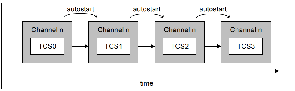
Here a DMA channel (n) is initially programmed for a DMA transaction. At the end of the DMA transaction the DMA automatically loads a new TCS from external memory (such as DSPR, LMU or PFLASH) and overwrites the channel TCS, and can start to execute it. At the end of this second DMA transaction, a third TCS is newly loaded and executed and so on.
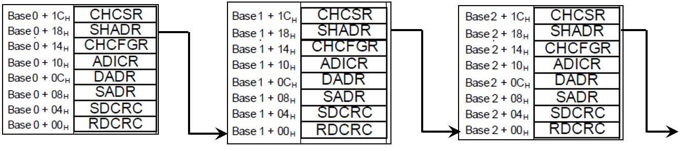
The DMA transactions in the linked list can be stored in any memory on the SRI bus, such as DSPR, PSPR, PFLASH, or LMU for example.
How this works is that the current DMA transaction uses the shadow address register (SHADR) as an address pointer to the next TCS. The address pointer to the next TCS must be mapped to a 32-byte aligned address.
That is, all DMA linked list TCSs stored in the memory shall be aligned to a 32-byte word. This is automatically guaranteed if they are in a contiguous memory area, and the first transaction is aligned to 32-bytes (since the size of a transaction control set is also 32-bytes).
Figure 4. DMA linked list operation
Accumulated linked list
The DMA accumulated linked list mode is chosen by setting ADICRz.SHCT = 0xD. It is exactly the same as a normal DMA linked list, except that the SDCRC and RDCRC checksums are accumulated over all the DMA transactions in the linked list.
Safe linked list
The DMA safe linked list mode is chosen by setting ADICRz.SHCT = 0xE. It is similar to the DMA accumulated linked list in the sense that the SDCRC and RDCRC are accumulated across DMA transactions.
However you are required to load the SDCRC word with an expected DMA Address Checksum value. As soon as the next TCS is read from memory, the DMA compares the DMA Address Checksum calculated by the current DMA transaction against the expected DMA Address Checksum stored in the next TCS. If the checksums match, then the DMA proceeds with the execution of the next TCS. If the checksums do not match then the Move Engine records a SAFLL DMA Address Checksum Error and triggers a DMA RP Error Interrupt Service Request. The DMA stops the execution of the linked list operation. Assuming all the DMA Address Checksum values match during the sequence of linked list operations then the DMA Address Checksum is calculated across all DMA transactions. The RDCRC is simply accumulated over all the transactions.
Conditional linked list
The DMA conditional linked list mode is chosen by setting ADICRz.SHCT = 0xF. It is an interesting feature because it is similar to executing an “if-else” condition. In this mode, in addition to the normal address pointer in the SHADR register, the SDCRC register acts as an address pointer, instead of storing the checksum.
The decision on which of these 2 pointers to fetch the next DMA transaction from, is made based on a pattern match on the read value.
During each DMA move the pattern detection logic determines the selection of the address pointer:
-
If PAT00 masked by PAT02 matches the DMA move data stored in MEm0R RD00 then as soon as the DMA move completes the ME shall load the DMA channel with the next TCS read from an address stored in SHADR.
-
If PAT01 masked by PAT03 matches the DMA move data stored in MEm0R RD00 then as soon as the DMA move completes the ME shall load the DMA channel with the next TCS read from an address stored in SDCRCR.
-
If both PAT00 masked by PAT02 and PAT01 masked by PAT03 match the DMA move data stored in MEm0R RD00 then as soon as the ME shall load the DMA channel with the next TCS read from an address stored in SHADR.
-
If there is no pattern match then the ME continues with the DMA transaction. If a pattern match is detected then:
- The DMA transaction ends with the current DMA move.
- The DMA channel TSR.CH will be cleared when the DMA write move has completed.
| SHCT | Linked list mode |
|---|---|
0xC | Normal linked list (DMALL) |
0xD | Accumulated linked list (ACCLL) |
0xE | Safe linked list (SAFLL) |
0xF | Conditional linked list (CONLL) |
Programming examples
In this section some coding examples are provided for the different DMA linked list modes. Note that in these programming examples, software triggering (Autostart) configuration is used. If hardware triggering is to be used for linked-list modes, the same code may be used but after setting the CHCSR.SCH = 0; CHCFGR.CHMODE = 1; and TSR.HTRE = 1. Additionally for a single transfer per hardware interrupt, the CHCFGR.RROAT shall be set to 0.
Linked list
In the simplest example of a linked list, a sequence of transactions is executed, as shown in Figure 5.
Here a DMA channel executes 3 different DMA transactions, programmed through TCSs tcs0, tcs1 and tcs2. These 3 DMA transactions have different configurations, such as different source/destination addresses, data width, transfer length, or move counts for example. The data lengths and the source and destination buffers of each transaction are shown in Figure 5.
Figure 5. DMA linked list example
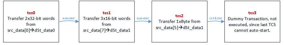
The last transaction (tcs3) is simply a dummy non-linked list transaction. This is required since a non-linked list transaction is never auto-started. Hence the last executable tcs (tcs2 in this case) has to be in linked-list mode. The dummy transaction could be replaced by tcs0 if the latter is configured to not auto-start (CHCSR.SCH = 0).
Allocation of the TCSs
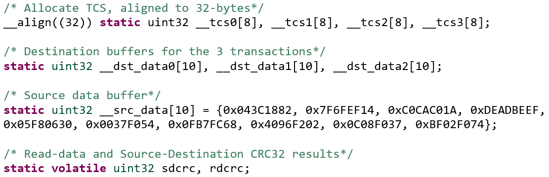
The various global buffers and variables used in the example code sequences are shown in Figure 6. As can be seen here the TCSs are allocated as arrays with 8x32-bit words, and aligned to 32-bytes.
Figure 6. Global variable declarations
Initialization of the TCSs
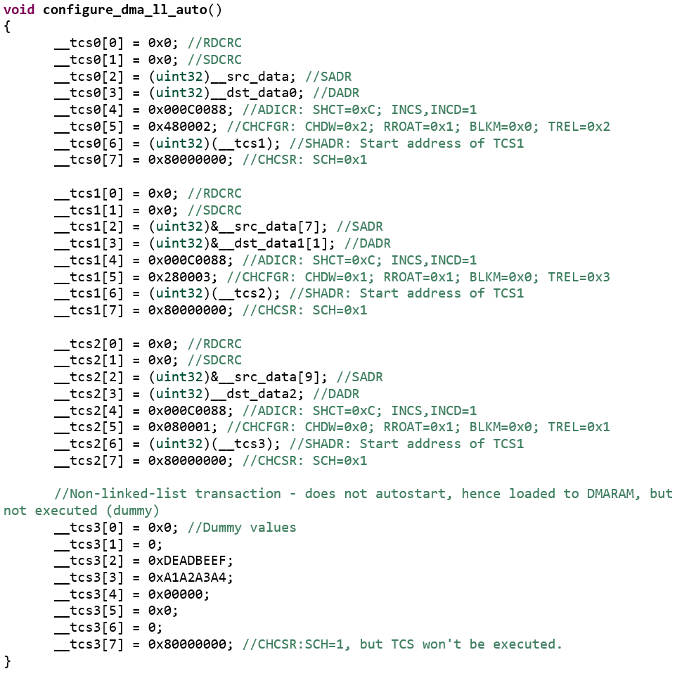
The TCSs are initialized according to the configurations shown in Figure 5. This initialization is shown in Figure 7 in the function configure_dma_ll_auto.
Figure 7. DMA linked-list initialization of the TCSs
Starting the linked list
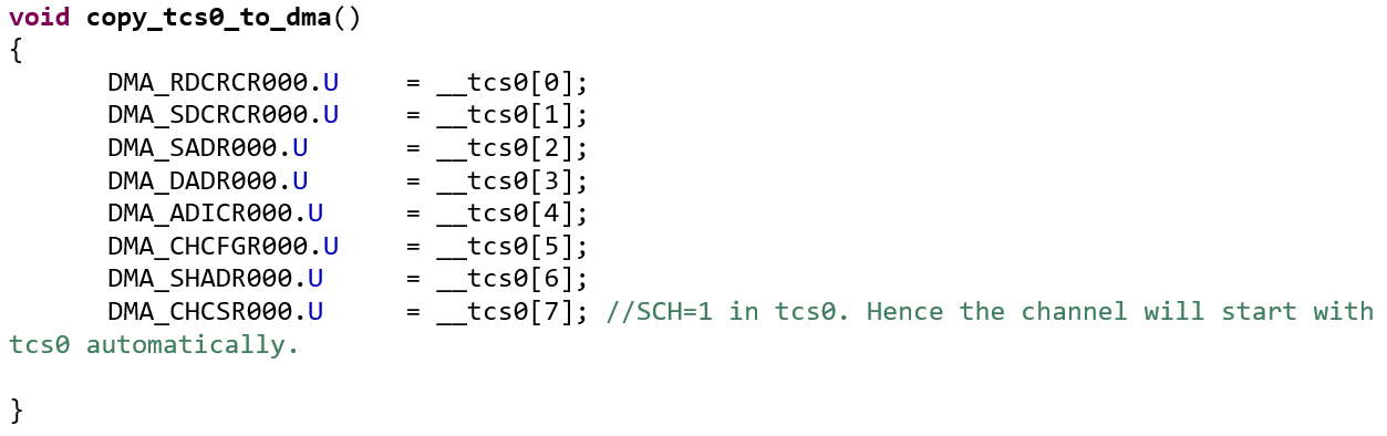
The linked-list is started by simply copying the TCS0 to any DMA channel. Since the CHCSR.SCH bit is set in all the TCSs, each DMA transaction will automatically start and execute its DMA moves, and will terminate after loading TCS3, which is not automatically started, since it is a non-linked list TCS.
The function copy_tcs0_to_dma in Figure 8 copies TCS0 to DMA Channel-0, so starting the linked list.
Figure 8. Starting the linked list; Copy TCS0 to DMA channel
In summary, to execute the linked-list:
-
Define the TCSs in memory, aligned to 32-bytes, and also the source and destination buffers.
-
Initialize the TCSs
- call the function configure_dma_ll_auto()
-
Trigger the linked-list
- call the function copy_tcs0_to_dma()
Results
After the execution of the DMA linked list, the destination buffers look as follows:
Figure 9. Destination buffer values after DMALL execution
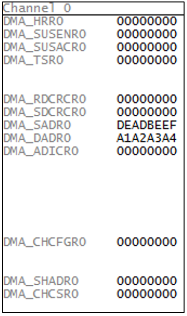
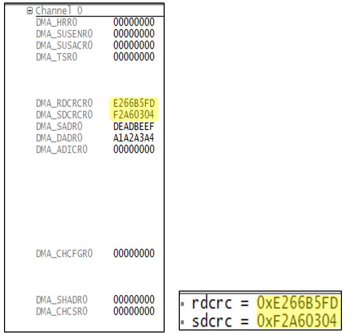
The DMA registers after the DMA linked list execution looks as shown in Figure 10. Note that the dmmy TCS (tcs3) has been loaded, but not executed.
Also note that the SDCRC & RDCRC values are 0; i.e. they are overwritten on a TCS load.
Figure 10. DMA channel register values after DMALL execution
Accumulated linked list
The accumulated linked list is similar to a normal linked-list as described in the previous section, except that the CRC values are accumulated across multiple TCSs and are not overwritten. This allows the software to check for safe operation.
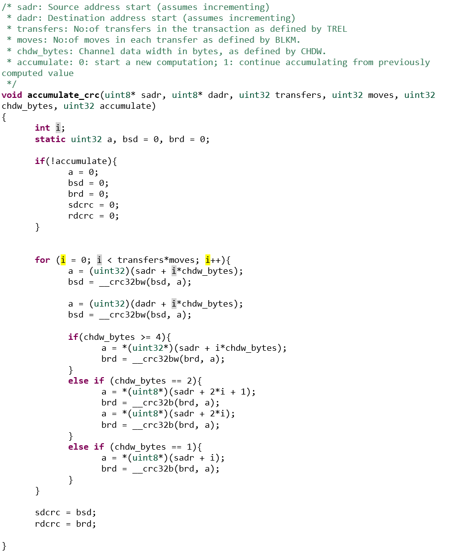
The function accumulate_crc shows an example of CRC computation for the DMA SDCRC and RDCRC. It takes as arguments, the DMA parameters such as source, destination addresses, transfer and move count for example, and calculates the RDCRC and SDCRC checksums. It is also possible to accumulate the computation across multiple calls (hence multiple transaction configurations). This function has been checked for data widths up to 32-bits.
Figure 11. CRC computation over transactions
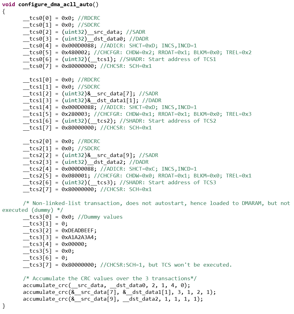
The CRCs can be pre-computed during the initialization of the TCSs. This is shown in the function configure_dma_acll_auto.
Figure 12. DMA Accumulated linked list configuration - with computation of CRCs.
The function call sequence to execute the accumulated linked list remains similar:
-
Define the TCSs in memory, aligned to 32-bytes, and also the source and destination buffers.
-
Initialize the TCSs and compute the CRC
- call the function configure_dma_acll_auto()
-
Trigger the accumulated linked-list
- call the function copy_tcs0_to_dma()
Results
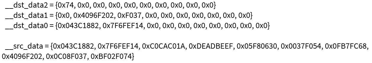
The data transferred with the accumulated linked list is the same as before, but what is different is the value of the CRC registers after the transaction finished. This is shown in Figure 13.
Figure 13. DMA channel registers after ACCLL execution and the SW computed CRCs
The CRC computed by calling the accumulate_crc function is also shown. As can be seen, the sdcrc and the rdcrc computed by software over all the transactions match the DMA result.
Safe linked list
A DMA safe linked list follows an accumulated linked list; i.e. the CRCs are accumulated over all the transactions in the linked list. The difference is that a new TCS is loaded only if the calculated SDCRCR matches the value stored in the next TCS.
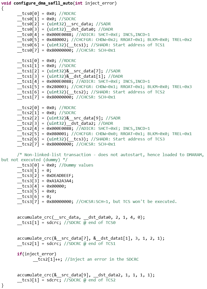
The configure_dma_safll_auto configures a safe linked list and also gives the possibility to inject an error and test it, by setting the inject_error argument to 1.
Figure 14. Safe linked list configuration example
The function call sequence to execute the safe linked list remains similar:
-
Define the TCSs in memory, aligned to 32-bytes, and also the source and destination buffers.
-
Initialize the TCSs and compute the CRC
- call the function configure_dma_safll_auto(<argument>) with 0 as argument for no error, and 1 to inject an error.
-
Trigger the safe linked-list
- call the function copy_tcs0_to_dma()
Results
Without any error (configure_dma_safll_auto(0)) then the results are similar to the accumulated linked list. Please refer to Figure 13.
However when configure_dma_safll_auto(1) is called (so the error injection is enabled), then the output is as follows:
Figure 15. DMA Channel registers and Destination buffers after SAFLL error.
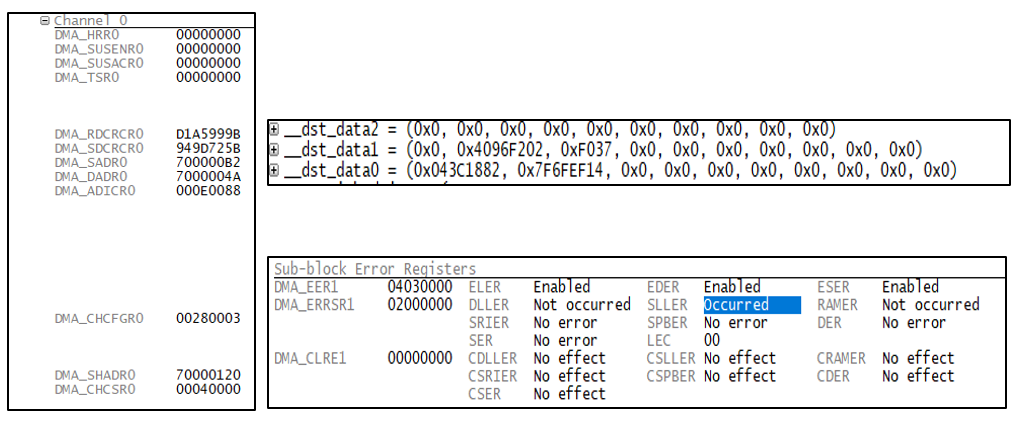
As can be seen in Figure 15, the DMA did not execute TCS2, since the SDCRCR did not match the expected value. Correspondingly, the SLLER bit in the ERRSR1 register is set, indicating that a DMA safe linked list error occurred.
Conditional linked list
A simple way to imagine the DMA conditional linked list is as an ‘if-else’ condition based on a transferred byte value. In the example shown in Figure 16, TCS0 initially transfers 16 bytes. Whenever a transferred byte matches 0x3X (i.e. the MSB nibble in the byte = 0x3, LSB nibble is don’t care), then TCS0 is finished after the DMA move, and the next DMA transaction is loaded.
When the pattern in question (here 0x3X) is matched in PAT[0] masked by PAT[2], then the next TCS is loaded from the address pointed to by SHADR. If the matched pattern is programmed in PAT[1] masked by PAT[3], then the next TCS is loaded from the address pointed to by SDCRCR.
Figure 16. Conditional linked list example
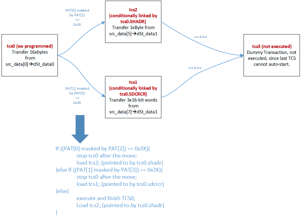
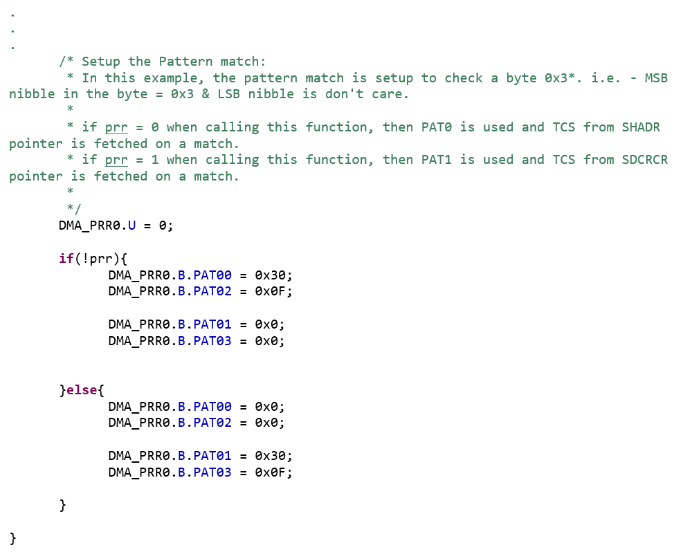
Figure 17 shows the implementation of configure_dma_conll function and configures the example shown in Figure 16. The argument of the function can be set to 0 or 1 to choose whether the pattern match is programmed in PAT[0] or PAT[1] (i.e. whether tcs2 or tcs1 is loaded on the condition match) respectively.
Figure 17. Configuring conditional linked list- part1
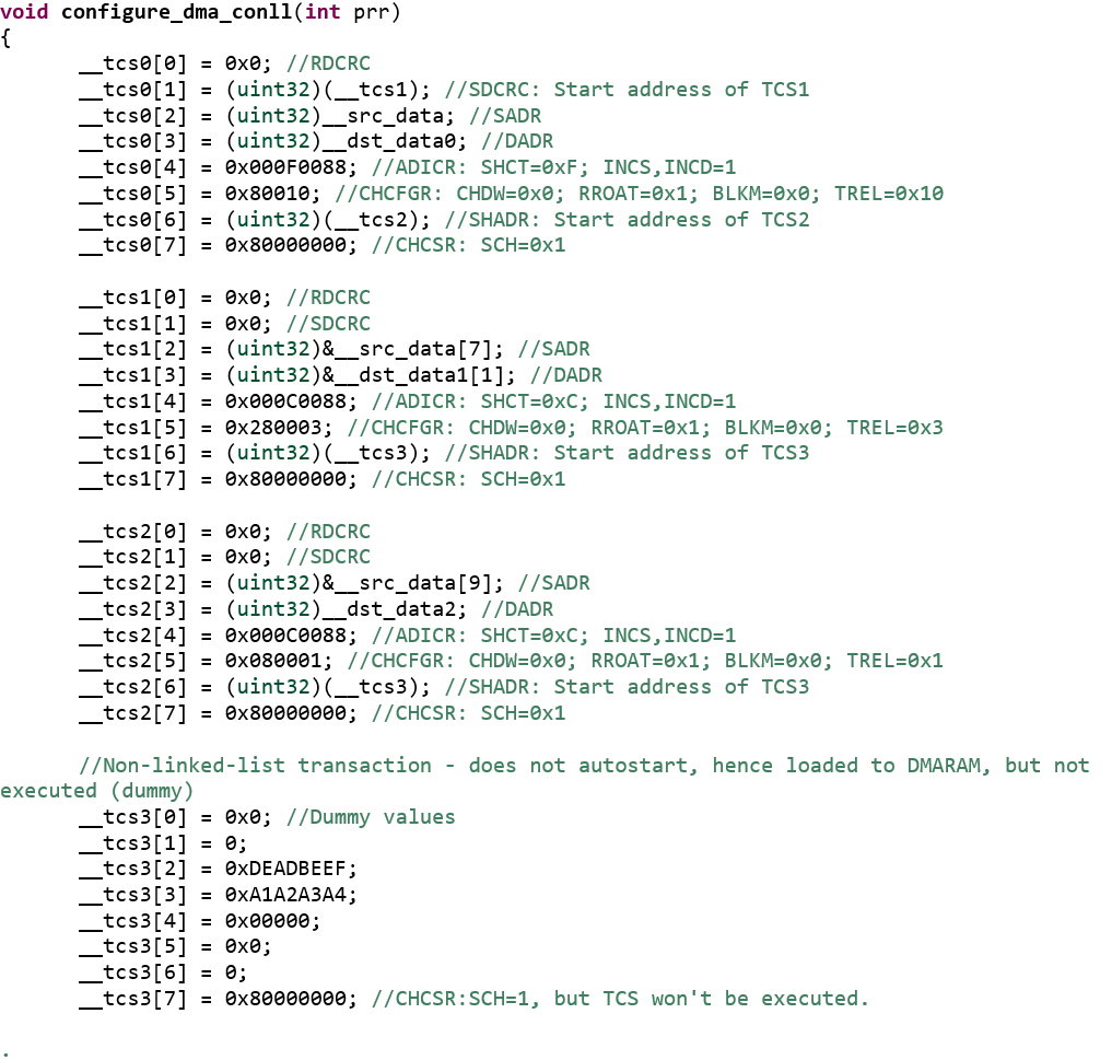
Figure 18. Configuring conditional linked list- Part2
The function call sequence to execute the conditional linked list remains similar:
-
Define the TCSs in memory, aligned to 32-bytes, and also the source and destination buffers.
-
Initialize the TCSs and pattern match registers
- call the function configure_dma_conll (<argument>), with 0 as argument to set the pattern match using PAT[0]/PAT[2], and 1 to set the pattern match using PAT[1]/PAT[3].
-
Trigger the conditional linked-list
- call the function copy_tcs0_to_dma()
Results
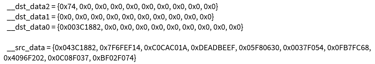
First, the DMA conditional linked list is executed by setting the pattern match condition in PAT[0] and PAT[2], so the function configure_dma_conll is called with argument 0.
The results are as shown in Figure 19. Note from the values in __dst_data0 buffer that the tcs0 stopped executing after transferring the byte 0x3C; since the pattern match condition 0x3X matches. Hence tcs2 is next executed and finished.
Figure 19. CONLL execution result with configure_dma_conll(0)
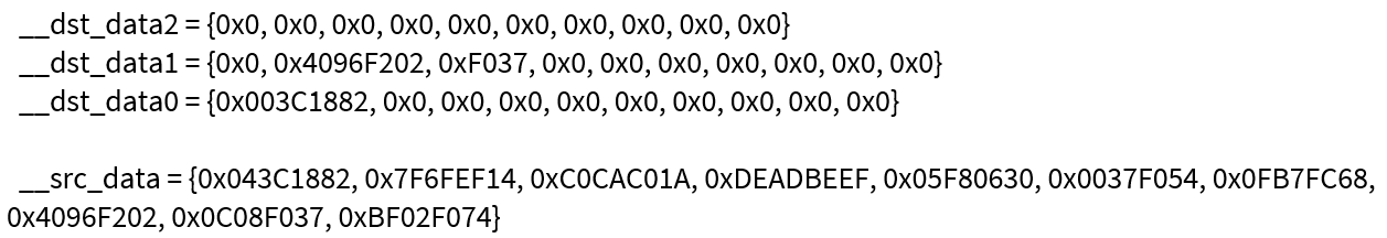
Second, the conditional linked list is executed by setting the pattern match condition in PAT[1] and PAT[3] (i.e. function configure_dma_conll is called with argument 1).
The results are as shown in Figure 20. Note from the values in __dst_data0 buffer that the tcs0 stopped executing after transferring the byte 0x3C; since the pattern match condition 0x3X matches. Hence tcs1 is next executed and finished.
Figure 20. CONLL execution result with configure_dma_conll(1)
Revision history
Document revision | Date | Description of change |
|---|---|---|
1.0 | January 2019 | First release |
V1.1 | 2024-04-17 | Template update Removed Note from the Results section |