AN1102 FuSa in a nutshell - HV-LV DC DC converter with AURIX™ TC3xx
32-bit TriCore™
AURIX™ TC3xx microcontroller
About this document
Scope and purpose
As requirements from functional safety standards in automotive, industrial and other fields are a challenging subject, this document intends to provide a first set of guidelines for users who are unfamiliar using the AURIX™ TC3xx microcontroller unit (MCU) in a functional safety scope.
This application note is part of a series of document named “FuSa in a nutshell” and listed in
3
.
Intended audience
This application note is intended for all those evaluating the AURIX™ TC3xx MCU, including functional safety engineers on the customer side and application engineers. This includes designers of safety-related systems who:
Are new to functional safety
Want to know more about functional safety (also called “FuSa”) applications
Want to understand in principle how functional safety can be implemented with hardware support
Are looking for functional safety details that cannot be found in the MCU user manual
Structure of the document
This document wants to provide a first guidance on the following safety related arguments:
HV LV DC-DC system and safety considerations
Chip set (when possible) for an ASIL D use case
New trends
Disclaimer
Information included in ths document are for training purposes only and are not to be taken as a blueprint for productive development.
ISO 26262 – HV-LV DC/DC converter
The most important system-level blocks of a powertrain system in an electric vehicle (EV) are the electric motor itself, the traction inverter drive, the DC/DC converter, the high-voltage battery and the on-board charger (OBC).
The architecture of electric vehicles comprises at least one low-voltage sub-network with low-voltage energy storage and multiple electrical loads and one high-voltage sub-network with high-voltage energy storage.
The HV/LV DC-DC converter’s function is to enable the energy flow between these two electrical subnets.
Typical design challenges are achieving the greatest efficiency possible and keeping the overall system costs under control. The space required for the DC-DC converter should also be kept as minimum as possible. Infineon’s portfolio is specially designed to help overcome these barriers easily.
The DC/DC converter system
is described in detail in the subsequent sections. This system needs to ensure that the right voltage is fed to the LV battery of the car, converted from the HV rail.
As stated in
2
, “the relevance of safety applications within the automotive industry is increasing continuously due to vehicle automation and decreasing relevance of mechanical backups. To cope with these trends, the power input of safety-related electrical and/or electronic systems needs to be ensured by the power supply system – leading to increased functional safety requirements. Compliance with ISO 26262 standard will be more in focus in the future.
The power supply system is a crucial point since faults of the power supply system are currently the major contributor for vehicle breakdowns with increasing tendency. So far, there is no standard approach within the automotive industry how to ensure functional safety for power supply systems.
Whereas today’s development focuses mainly on voltage stability and load balance, the future activities shall also include the system’s behavior under various fault scenarios to ensure ISO 26262 compliance.
The essential safety requirement – beside the safe power feed and safe power distribution – is to assure the freedom from interference between the safety and non-safety relevant components.”
DC-DC Topology overview and selection
The choice of the topology for a high voltage-low voltage converter application in automotive on-board charging depends on several factors such as efficiency, power density, and cost.
In the following section some of the most common topologies like the Phase shift Full Bridge(PSFB) with different types of Sinchronous Rectifier (SR ) and Dual Active Bridge (DAB) converters will be briefly described.
Phase Shift Full Bridge converter
In the Phase Shift Full Bridge converter, the gate driving signals of the legs of the converter are characterized by a fixed duty cycle of 50%.
The power transferred to the secondary side is determined by the shift applied between the two legs of the primary side. Through the use of phase-shifted switching, the converter can achieve Zero Voltage Switching (ZVS), effectively reducing switching losses therefore achieving high efficiency and reducing electromagnetic interference.
Figure 1. Reference schematic for the Phase Shift Full Bridge topology
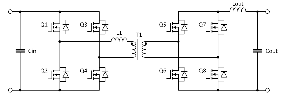
Various control methods can be applied to this specific topology, based on voltage or current control. The most commonly used are the current mode control, both average and peak current (ACMC and PCMC) as well as hybrid and predictive control algorithms.
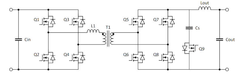
Dual active bridge (DAB) converter
A Dual Active Bridge functions as a bidirectional DC-DC converter with matching full-bridges on both the primary and secondary sides, along with a high-frequency transformer which provides galvanic isolation, an energy transfer inductor and DC-link capacitors.
Widely employed in applications such as solid-state transformers, transportation, and renewable energy systems, the dual active bridge converter is distinguished by its high efficiency, isolated operation, power density, and the capability to facilitate bidirectional power flow.
Figure 2. Reference schematic for the dual active bridge topology
After the topology has been described, a description of the most common
control methods
for the switches is given. There are also many variations where different control methods are combined, depending on power and voltage range.
Single-Phase Shift Modulation (SPSM) serves as a widely adopted method for modulating the Dual Active Bridge (DAB) due to its simplicity. This approach involves adjusting the phase shift between the primary and secondary side of the DAB while maintaining a 50% duty cycle. One notable advantage of this modulation technique is its straightforward control mechanism.
However, it's important to note that this control technique comes with its own set of drawbacks, like reactive current losses in wide voltage range conversion and a restricted zero voltage switching (ZVS) range.
There are multiple other modulation techniques that allow to reach better performance but are more complicated in terms of control algorithms like the Extended Phase Shift Modulation (EPSM) or the Dual Phase Shift Modulation (DPSM). Each of these modulations presents its own set of advantages and disadvantages.
Secondary side in depth study
In Phase Shift Full Bridge DC-DC converters, the selection between diodes and MOSFETs on the secondary side changes the operational dynamics but also the efficiency and performance of the converter.
Diode rectification on the secondary side of a DC-DC converter provides a simple and cost-effective means of rectifying. However, they are associated with inherent conduction losses, particularly at higher output currents and lower output voltage levels. This can lead to reduced efficiency and increased thermal dissipation, especially in applications with demanding load conditions
The deployment of switches (MOSFETS or wide bandgap switches) for synchronous rectification on the secondary side enhances the efficiency and performance of DC-DC converters. Switches, when integrated as active switches for rectification, offer lower conduction losses compared to diodes. This is particularly advantageous in systems with low output voltage and/or high output current ratings, where reducing losses is very important for achieving optimal efficiency. Furthermore, switches enable the implementation of advanced control schemes, which can further enhance the overall performance and efficiency of the converter. For further analysis on switches selection please refer to clause
Switches selection
In the past, diode rectification sufficed for projects prioritizing simplicity and cost-effectiveness. However, in modern days systems where efficiency and precise rectification are crucial, MOSFETs have become the preferred choice, especially in modern high-voltage to low-voltage DC-DC converters.
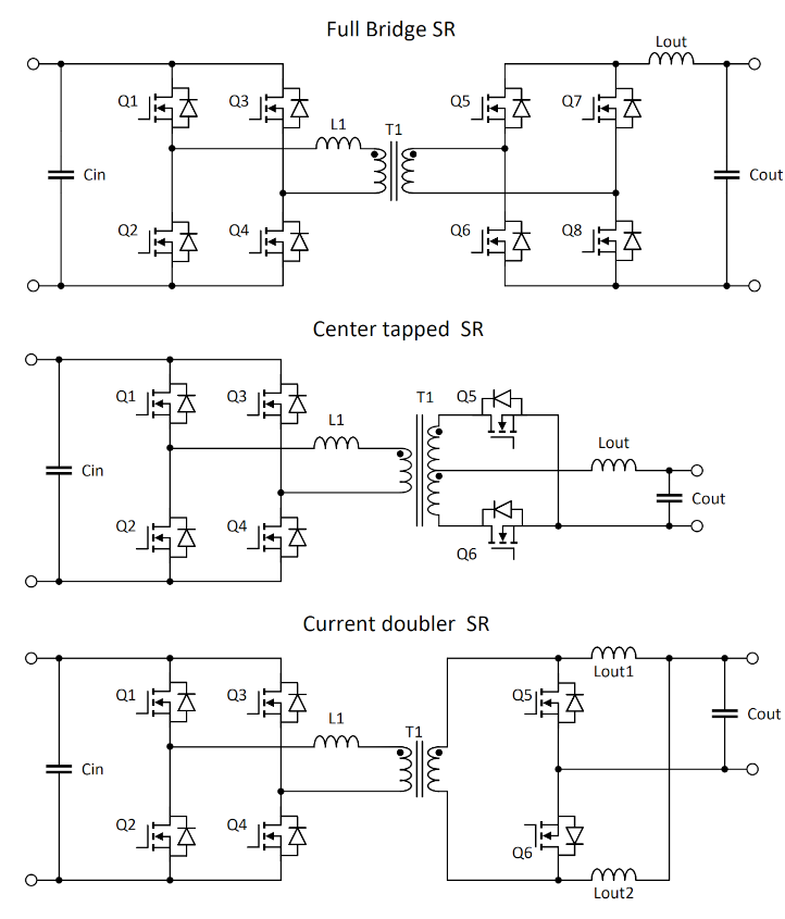
Phase shift full bridge rectifier types
The PSFB converter can be changed on the secondary side adopting different rectifier topologies.
The rectifier is usually chosen between three commonly used topologies:
Full Bridge
This configuration is also commonly called half bridge – half bridge configuration due the positioning of the swithches, whereas the other two following configurations are also called common source configurations for the same reason.
This configuration will also be analyzed as the system reference topology for the following sections.
Center tapped
In this rectifier topology a center tapped transformer is used. This type of transformer is designed to produce two secondary voltages with a common connection at the center of the secondary winding. The center tap serves as the reference point, dividing the winding into two symmetric halves. Each half of the winding corresponds to a phase of the AC waveform, enabling the rectification process.
This rectifier topology is commonly used when the secondary side of the converter present low voltages with respect to the primary side.
Current doubler
This rectifier employs two output inductors, each responsible for carrying half of the total load current. This arrangement not only allows for better heat dissipation distribution but also necessitates current-mode control as a fundamental requirement for the current-doubler rectifier, therefore his topology is commonly used when secondary side deals with very high current values.
Figure 3. Reference schematic for center tapped rectifier
DC-DC use case initial assumptions
In the following section the assumptions made in the described DC-DC use case are described.
It is required that the
12 V battery can be isolated from the DC-DC converter
in case of a fault happening, this is why a switch implemented in a back to back (B2B) configuration (clause
LV back-to-back (B2B) Gate diver for output switch
) is placed at the output of the converter right before the connection with the 12 V battery. In this way the voltage supply can be detached from the battery when a fault is detected in the converter.
The DC DC converter will be ASIL rated for the power supply to the battery.
To support the metrics demanded from this ASIL rating, the battery disconnect on the 12 V side is added.
In this way, if a fault is detected and the system cannot provide the 12 V supply to the battery, it should be disconnected, making it fail silent and leaving the 12 V battery to deliver the power to the LV grid until it is discharged completely.
Following assumptions for the electronic control unit are made:
Overvoltage category: II
Pollution degree: 2
Material group: I
High voltage side: 800 V class
Low voltage side: 14 V
Voltage and current sensing for both high and low voltage sides
Overcurrent pin to pin reaction time (FTTI):
200 ns
The
safe state
for the high side whenever there is a fault into the system is to put the high side of the bridges in an open condition, while the lower switches close. This condition allows the inductor to discharge to ground the energy stored, avoiding the hazard of a charged inductor in an off-system condition.
Another commonly implemented solution for the safe state is to open all switches allowing for remaining charge to flow through the body diodes of the switches.
The “slow” hazards can be easily controlled by SW, while ultra-fast component protection measures usually require further HW safety countermeasures.
Safety Requirements
The safety requirements related to the power converter are derived from the safety goals of the systems that are powered by the DCDC converter. It is possible for example to consider the Safety requirement designed for the EPS (Electrical Power steering) as described in
2
:
“SRx: Prevent sudden loss of steering assist due to failure in power
supply – for example: ensure power supply stays within defined voltage/time
intervals.
Regarding the power supply sub-system level, there are three major topics to address:
SRx.1 –
Power feed
: An energy source and/or storage must feed the electrical power for the electrical loads
SRx.2 –
Power distribution
: The wiring, fusing and switches of the power supply system must distribute the electrical power from the energy source/storage to the electrical loads
SRx.3 –
Freedom from interference
: Electrical loads, the physical power supply system components and the power supply management must not interfere with the power supply by violation of SR2. The freedom from interference between sub-elements implementing functions with different ASIL ratings is a basic principle of ISO 26262
These High-level safety requirements can be seen as the allocation to the sub-system “power supply” of the Safety Requirement created at System level for the EPS.”
System use case overview
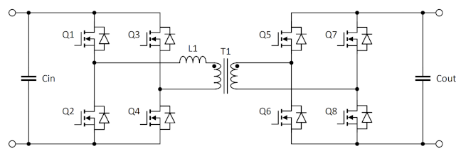
This document focuses on Phase Shifted Full Bridge topology with full Bridge rectifier and all the following sections will be based on this specific kind of converter.
Figure 4. Simplified block diagram of the DCDC converter system
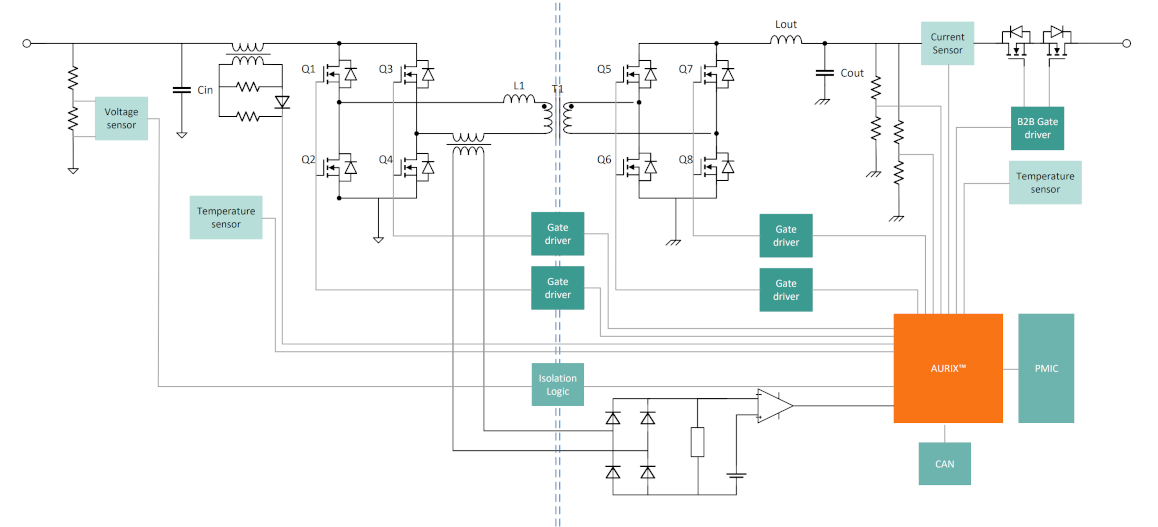
To
control
the voltage converter, Infineon’s
AURIX™ TC3xx
MCU
family implements advanced features for signal acquisition with the highest safety rating.
Surrounding the power stage that may contain
Si IGBTs or SiC MOSFETs
, there are driver devices that translate the signals to or from the MCU and provide the necessary
isolation
.
To provide the
power supply
to the AURIX™ TC3xx MCU, Infineon
OPTIREG™
power management IC (PMIC) products offer integrated solutions specifically for the harsh automotive environment.
Current and voltage sensing
both in primary and secondary side, provide the necessary feedback for precise and energy efficient converter control.
Isolation between high and low voltage
The electrical isolation rating of a system is vital for its proper functioning and safety.
There are three levels of isolation ratings for electrical systems as well described in the IEC vocabulary:
functional insulation
IEV ref 195-02-41: insulation between conductive parts, necessary for the proper functioning of the equipment
normal condition
IEV ref 903-02-07: condition in which all means of protection are intact
basic protection
IEV ref 195-06-01: protection against electric shock under normal conditions
basic insulation
IEV ref 195-06-06: insulation that provides basic protection
supplementary insulation
IEV ref 195-06-07:independent insulation applied in addition to basic insulation, that provides fault protection
double insulation
IEV ref 195-06-05: insulation system comprising both basic insulation and supplementary insulation
reinforced insulation
IEV ref 195-06-09: insulation that provides a degree of protection against electric shock equivalent to double insulation
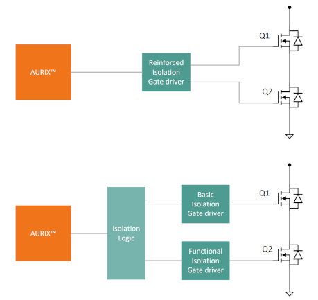
The isolation topic is particularly relevant for the gate drivers and digital isolators selection when dealing with the high voltage side. There are two main ways of implementing the required isolation level when evaluating the components selection:
Reinforced isolated gate driver
Functional isolated gate driver at the low side, basic isolated gate driver at the high side, both paired with digital isolator IC
Figure 5. Two ways to perform gate driving on HV side
Hardware components
The major requirements and the key features of the selected components are:
AURIX™ TC3xx MCU family, the converter control core
Power supply for the entire system using a PMIC and other power supply converter such as low-dropout regulators (LDO)
Digital isolators
Gate drivers for the the four Si IGBTs, Si SJ or SiC MOSFETs Power switches (high and low voltage) as well as for the Back to Back switch configuration
Current Sensing circuitry
Temperature sensors: For PCB- and heatsink or case temperature
Voltage sensing circuitry
CAN (-FD) Transceiver for communication with the vehicle
Operational amplifiers and digital comparators
AURIX™ TC3xx MCU
To control the HV-LV DCDC converter, Infineon’s AURIX™ TC3xx MCU family offers up to hexa-core performance and advanced features for signal acquisition and pattern generation, connectivity, security and functional safety, ensuring it is ideally suited for many automotive applications, including DCDC converters control.
The AURIX™ TC3xx microcontroller enables the implementation of complex control algorithms and safety measures crucial for high voltage-low voltage DCDC converter applications. Through a closed-loop control scheme, the AURIX™ TC3xx MCU supports the exact switching control of the converter.
The AURIX™ microcontroller offers a comprehensive peripherals portfolio as the GTM ATOM for PWM generation, EVADC and EDSADC for current and voltage sensing, communication peripherals to interface with voltage sensing, temperature sensing, and CAN communication integrated circuits. These peripherals can be effectively utilized to control a DCDC converter, enabling precise regulation and monitoring.
The GTM (Generic Timer Module) ATOM within the AURIX™ microcontroller provides advanced capabilities for PWM (Pulse Width Modulation) generation. In the context of controlling a DCDC converter, the GTM ATOM modules can be configured to produce the necessary PWM signals for driving the converter's power switches. By adjusting a combination of duty cycle, phase shift and frequency of the PWM signals, the converter's output voltage can be regulated effectively.
The EVADC (Enhanced Versatile ADC) and EDSADC (Enhanced Delta-Sigma ADC) modules of the AURIX™ microcontroller facilitate accurate voltage and current sensing, a critical aspect of DCDC converter control. The acquired current can then be utilized for implementing closed-loop control algorithms, enabling precise current regulation and overcurrent protection in the DCDC converter.
The CAN communication interface is essential in the system, as it enables the microcontroller to communicate with other system components, providing control command, status report, diagnostic capabilities and fault notifications within the DCDC converter system. More on the AURIX™ TC3xx MCU can be found into the device User’s Manual
1
.
AURIX™ TC3xx MCU power supply
The power management IC device can manage and monitor the various power supplies of a complex MCU.
One important functional safety feature of this integrated circuit is its ability to detect and report faults in the power supply, such as overvoltage, undervoltage and overcurrent conditions. The device includes a range of built-in protection mechanisms, such as voltage and current clamping, to help preventing damage to sensitive electronic components in the event of a fault.
The power supply circuit chosen for our use case also includes several features to help ensure reliable and stable power delivery to critical vehicle systems, including multiple regulated outputs, each of which can be programmed to a specific voltage and current limit. Another relevant safety feature is the presence of a time-window watchdog to monitor the system for malfunctions and automatically reset the device if the MCU is not responding in the right manner.
Additionally, the MCU power supply can request a safe state (independently from the MCU) if it is assumed that the MCU is not working properly. This is a redundant safety path.
In addition to its functional safety features, a good power supply integrated circuit is designed to be highly efficient and reliable. The device is capable of operating at high temperatures (the ambient temperature is often defined in a range between -40°C and 85°C) and include advanced thermal protection features to prevent damage from overheating.
Figure 6. Infineon TLF35584 safety connections of the power supply module (besides needed supplies)
provides an example of connections needed for functional and safety purposes when using the TLF35584 PMIC as a power supply chip. As Infineon is permanently expanding the portfolio with dedicated chips and solutions, check the company website or the regional support for the newest chipset.
Besides the power supply of the AURIX™, the power supply IC also has a supervision function for the microcontroller. During operation, the MCU and the power supply IC are exchanging signal patterns to check if the MCU is still in the right operation and is trustworthy. If the power supply IC is receiving the wrong pattern several times, an MCU power removal can be forced as a safe reaction.
If the MCU cannot be assumed to be trustworthy for executing the right PWM pattern and actions, the power supply IC uses its SS1 and SS2 pins to force the system into a safe state without having to rely on the MCU’s functionality. This redundant safety path is a basic need to enable an ASIL-compliant design.
NR | AURIX™ | PMIC | Description |
|---|---|---|---|
1-4 | SPI- pins | SPI- Pins | SPI data transmission for configuration and data readout in a bidirectional way |
5 | FSP | ERR | Diagnostic output signal from AURIX™ TC3xx to TLF to activate an independent safety path |
6 | ESR1 | INT | Safety output from PMIC to AURIX™ |
7 | PORTX.Y | WDI | Watchdog input signal from AURIX™ |
8 | PORST | ROT | Reset to AURIX™ |
9 | PORTA.B | SS1 | For the startup test of SS1 output effectiveness (optional) |
10 | PORTC.D | SS2 | For the startup test of SS2 output effectiveness (optional) |
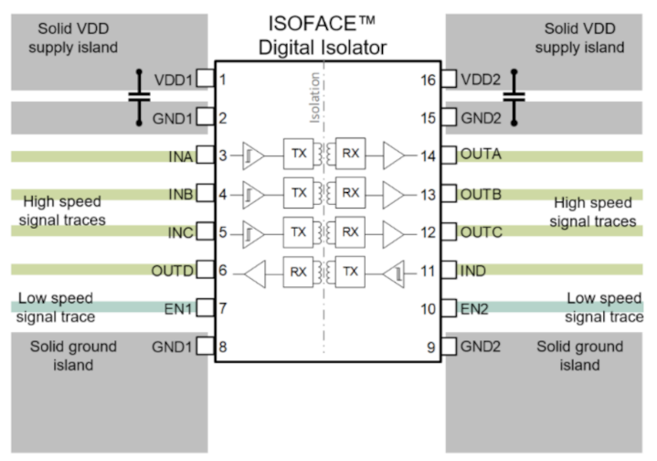
ISOFACE™ Digital Isolators
Digital isolators play a critical role in ensuring the safe and reliable operation of electronic systems. These isolators protect sensitive circuits from potentially harmful electrical signals, such as noise, transients, and ground loops, and provide electrical isolation between different parts of the system.
DCDC converters are used to step down the high voltage of the battery to a lower voltage that is suitable for charging the low-voltage battery in a hybrid or electric vehicle. These converters require robust isolation between the high- and low-voltage sides of the circuit to protect against potential hazards.
Infineon Technologies provides the 4-channel ISOFACE™ digital isolators to perform the digital isolation required for this specific application and the main characteristics of these devices are:
Reinforced isolation:
This means that the isolators have been designed to withstand high voltages and provide increased protection against electrical hazards. Reinforced isolation ensures that the isolators are able to provide reliable and safe operation in harsh or unpredictable environments
Minimum creepage distance of 8mm:
Creepage distance refers to the distance between two conductive parts of a circuit and is an important consideration when designing electrical systems that require isolation
High isolation withstand voltage:
Isolation withstand voltage refers to the maximum voltage that an isolator can withstand without breaking down or otherwise failing
Figure 7. Infineon ISOFACE™ Digital Isolators
HV Gate drivers
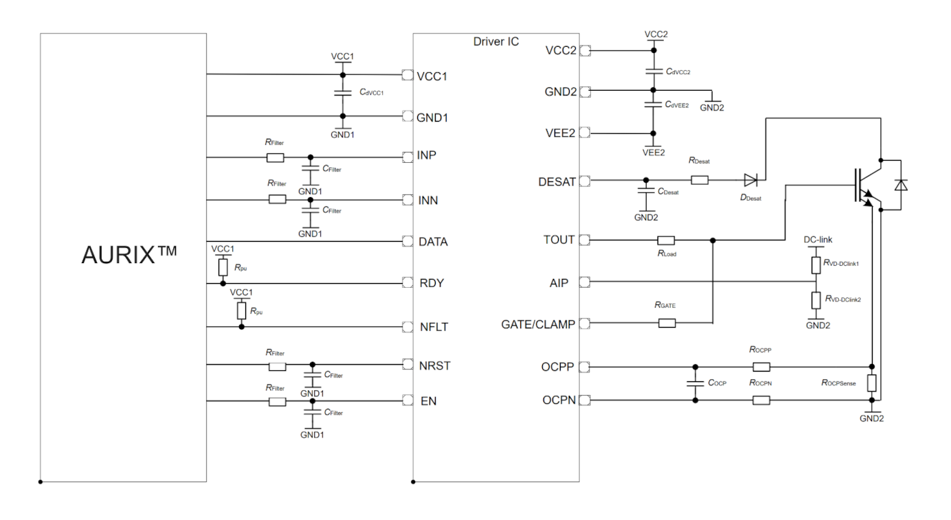
The EiceDRIVER™ 2EDR9259X is a reinforced isolated gate driver IC designed to provide control over a safe isolation barrier.
It features a strong source/sink dual-channel gate driver and offers a very high CMTI (common mode transient immunity) for robust operation in CoolSiC™ and high-power switching noise environments. Additionally, it provides a very short propagation delay with low variation over temperature and production, enabling power system designs to achieve higher efficiency through precise timing control across the safety isolation barrier.
Figure 8. EiceDRIVER™ 2EDR9259X connection schematics
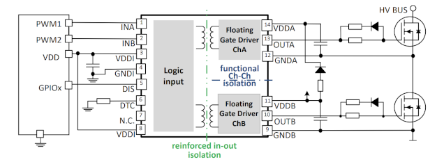
To evaluate the impact of the described functionality on the system in terms of required pins, the Infineon 2EDR9259X is considered.
needs to be repeated two times for the four IGBTs or MOSFETs to consider the correct pinout of AURIX™ TC3xx.
NR | AURIX™ | Gate driver | Description |
|---|---|---|---|
1 | GTM-(A)TOM | INA | PWM input comes from the GTM timer output module (ATOM or TOM channel). The input signal is transferred non-inverted to the corresponding gate driver output OUTA. |
2 | GTM-(A)TOM | INB | PWM input comes from the GTM timer output module (ATOM or TOM channel). The input signal is transferred non-inverted to the corresponding gate driver output OUTB. |
3 | GPIO | DIS | Disable input channel A and B. It comes from an AURIX™ GPIO output pin. |
The presented Integrated circuit is not ASIL rated but it has been included in the description since it is the commonly used product from the portfolio in this Application. For ASIL rated products considerations and argumentations please refer to section
System use case overview
.
LV Gate drivers
Choosing the gate driver for the secondary side does not involve isolation since the domain in which these components work is the same as the microcontroller.
EiceDRIVER™ 2EDF7259KQ1 is a dual-channel gate driver IC designed to drive Si MOSFETs and GaN HEMTs. The product is available in a 13-pin LGA package with 3.4 mm input-to-output creepage and provide basic isolation by means of on-chip coreless transformer (CT) technology.
2EDF7259KQ1 offers optional shoot-through protection (STP) and dead-time control (DTC) functionality; this allows the operation as dual-channel low-side, dual-channel high-side or half-bridge gate driver with a configurable dead-time. With an excellent common-mode transient immunity (CMTI), low part-to-part skew and fast signal propagation.
Figure 9. EiceDRIVER™ 2EDF7259KQ1 connection schematics
To evaluate the impact of the described functionality on the system in terms of required pins, the Infineon EiceDRIVER™ 2EDF7259KQ1 is considered here.
needs to be repeated two times for the four IGBTs or MOSFETs to consider the correct pinout of AURIX™ TC3xx.
NR | AURIX™ | Gate driver | Description |
|---|---|---|---|
1 | GTM-(A)TOM | INA | Logic PWM input signal |
2 | GTM-(A)TOM | INB | Logic PWM input signal |
3 | GPIO | ENABLE | Disable input channel A and B. It comes from an AURIX™ GPIO output pin. |
The structure of the specific synchronous rectifier implemented also influences the gate driver selection, in this example the full bridge rectifier is considered and for this reason the EiceDRIVER™ 2EDF7259KQ1 has been selected. If another kind of rectifier is implemented into the system, like the center tapped or current doubler SR, low side gate drivers can be chosen.
The presented Integrated circuit is not ASIL rated but it has been included in the description since it is the commonly used product from the portfolio in this Application. For ASIL rated products considerations and argumentations please refer to section
System use case overview
.
LV back-to-back (B2B) Gate diver for output switch
Two MOSFETs are placed at the output of the converter in a back-to-back configuration that is used to detach the low voltage battery from the converter in case of fault of the system. To drive these MOSFETs a gate driver must be selected.
The AUIR3241STR is a high-performance gate driver IC designed specifically for use in back-to-back applications, making it an ideal choice for driving two MOSFETs in this configuration.
This integrated circuit features a range of advanced features, these include an advanced input filter for noise immunity, a high current output stage for fast switching, and an integrated bootstrap diode for reduced component count.
One of the key advantages of using the AUIR3241STR to drive two MOSFETs back-to-back is its ability to handle high peak output currents. This makes it well-suited for use in high-power applications, where reliable and efficient power management is critical.
Figure 10. Back to back gate driver connection schematics
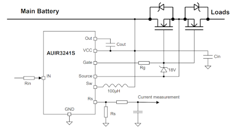
In the following table the connection between the gate driver and the microcontroller is described.
NR | AURIX™ | Gate driver | Description |
|---|---|---|---|
1 | GPIO | IN | Command for gate driver actuation |
2 | EVADC | Rs | Analog output current measurement |
The need of the back-to-back topology for the output switch depends on the safety requirements of the system implementation.
Adopting B2B solution can also help in protecting the low voltage battery from voltage spikes resulting from faults on the regulation loop, protecting from unwanted activations of a single switch performing the reverse polarity protection.
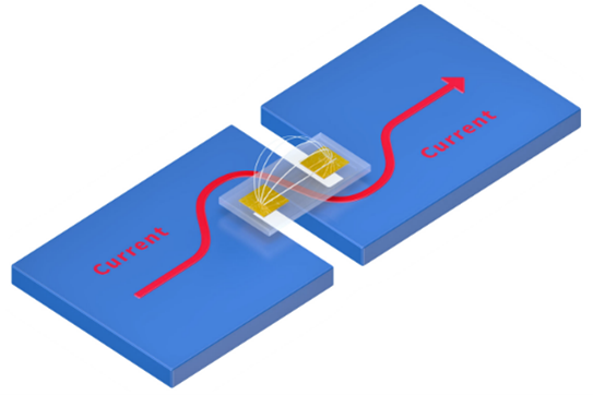
Current measurement secondary side output
The TLE4973 current sensor from Infineon is a highly reliable and functionally safe solution designed for accurate current measurement. It offers a range of features to ensure safety and precise operation.
Figure 11. Current sensing example: Lateral sensor insertion
The sensor is equipped with an over current detection (OCD) pin, enabling efficient monitoring and protection against excessive current levels. This pin provides an additional layer of safety by allowing the system to quickly respond and mitigate potential risks associated with overcurrent conditions. The sensors can be configured by the customer for specific thresholds and deglitch timings.
The OCD pin is designed as open-drain output and can be connected to the logic input pins of the MCU and/or the pre-driver to quickly react to over-current events.
All user-programmable parameters such as OCD threshold blanking times and sensitivity settings are stored in an embedded EEPROM memory. Device configuration can be performed in-situ through an UART based bus compatible one wire interface called Digital Control Diagnostic Interface (DCDI). The DCDI interface provides read/write access to internal registers of the device and allows to trigger the diagnostic mode and to read temperature, OCD and safety status. It has an auto-addressing functionality and can handle up to 8 slaves on one bus, meaning that multiple current sensors can be connected to the same microcontroller pin.
Another notable feature is the configurable analog output operational mode. It offers flexibility in selecting the operational mode, whether fully differential or single-ended. This adaptability enables seamless integration into different system architectures, catering to specific application requirements and optimizing overall performance.
Figure 12. Application circuit for Infineon TLE4973 current sensor, single-ended and fully differential
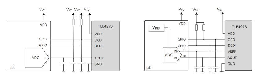
The current sensor combines precise current measurement, independent overcurrent detection pins, configurable operational modes and a robust design compliant to functional safety rating (ISO 26262 ASIL B).
To evaluate the pin requirements of the system implementing the current sensing functionality, the Infineon TLE4973 is considered as a reference.
shows connections with a current sensor in differential mode connection.
NR | AURIX™ | Current Sensor | Description |
|---|---|---|---|
1 | EDSADCx | VREF | Reference voltage I/O, analog output signal in fully differential mode, synchronized with ATOMs PWM pattern to the gate driver input to AURIX™ TC3xx delta sigma ADC module |
2 | EDSADCx | AOUT | Analog output signal (for TLE4972): Input to AURIX™ TC3xx delta sigma ADC module |
3 | GPIO | OCD | Over-current detection output (open drain output) |
4 | ASCLIN | DCDI | Diagnostic interface |
It is important to make the following general considerations about current measurements:
As a Safety Element out of Context (SEooC), the AURIX™ TC3xx safety concept will require ADC redundancy for analog acquisition
Since the system presents several current measurements both in primary and secondary side, it is possible to perform some plausibility checks on the values that are read from the sensor with the other ones that the microcontroller is reading:
Zero crossing and current measures
The PWM gate driving pattern is known since it is computed into the AURIX™ TC3xx, so it is possible to know if the input current values are physically possible
The above-listed plausibility checks are useful to develop a good safety solution.
Other common-cause failures in ADC modules should be considered; for example, the analog voltage reference (VREF) requires a dedicated safety check that allows for the detection of unintended drift. Here, multiple solutions are feasible, such as using a redundant second VREF, which can be compared to the main one or the internal bandgaps of the MCU itself.
Further things to be checked from a safety perspective include, for example, broken wire detection. An indication of typical failure modes to be considered in an analog acquisition can be found in the MCU safety manual provided under non-disclosure agreement (NDA).
Temperature sensors
The temperature sensor is often implemented as an analog device specifically designed for accurately measuring the temperature of a board component or system part, enabling further safety monitoring and control. This is not a mandatory safety measure but is commonly used to check that the working temperature range of the system is not exceeded.
One important factor is accuracy, which should be maintained across a wide temperature range, allowing for effective monitoring in both extreme hot and cold conditions. The sensor's output represents the temperature being sensed, enabling easy interpretation and integration with existing systems.
To perform out-of-range detection within the AURIX™ TC3xx, the temperature sensor, its supply and the circuitry around it must be designed to ensure normal operation between 0.5 V and 4.5 V at the ADC pin of the AURIX™ TC3xx. This enables monitoring to determine if the signal is within this range or outside. If it is outside the range, a wire may be broken, or the supply may be missing. This is important to verify the plausibility of the measured temperature value. As for the purpose of this example the temperature is a “complementary” measure; it is therefore not considered redundant.
NR | AURIX™ | Temperature sensor | Description |
|---|---|---|---|
1 | EVADC | Vout | Voltage output for temperature value |
Note: AURIX™ TC3xx also offers die temperature sensors (DTS), which can be used from a safety concept perspective as a complementary source of input to perform plausibility checks.
Voltage sensor
To detect the voltage of the primary side an isolated integrated circuit is needed due to the high voltages involved.
The integrated circuit commonly used to accomplish this task is a precision delta sigma modulator that operates using external clock and power supply. The voltage measure is then sent to the microcontroller using a Pulse Density Modulated or Manchester encoded bitstream.
The voltage measurement is performed by an integrated circuit that is placed into the HV side of the system. To provide the right isolation to the microcontroller, before reaching the AURIX, the line is fed into an isolation logic integrated circuit, which then sends the signal to the microcontroller.
Figure 13. Voltage sensing IC connections with MCU
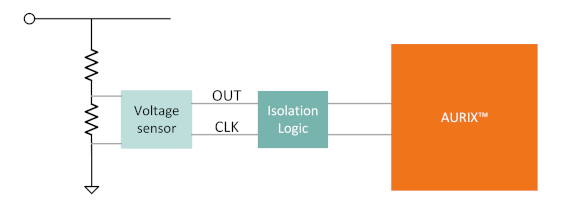
NR | AURIX™ | Voltage sensor | Description |
|---|---|---|---|
1 | EDSADC | OUT | Manchester/PDM coded output information on sensed voltage |
2 | EDSADC | CLK | Clock input to the integrated circuit |
CAN transceiver
To make the DC DC converter integrated within the entire car system, an integrated circuit that accomplishes CAN communication is needed. For this reason, a CAN transceiver must be selected to enable the AURIX™ TC3xx MCU to communicate using that specific bus protocol.
Some of the key features of a good CAN module are:
Fail-safe features such as TxD time-out, RxD recessive clamping and overtemperature shut-down, that allow the system to perform in a predictable manner in a safety-critical situation. Other safety measures also report the CAN short circuit proof to ground, battery and VCC, as well as undervoltage detection on the supply voltages
Local failure diagnostics should also be implemented by specifically designed output pins
Keeping into account the earlier mentioned characteristics of a CAN transceiver, the Infineon TLE9252V CAN transceiver is taken as a reference to understand how the CAN functionality can be integrated into the safe system itself.
Figure 14. TLE9252V CAN transceiver connections with MCU and power supply
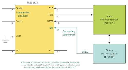
Referring to
Figure 14
, the connection required with the MCU is reported in
Table 8
.
NR | AURIX™ | CAN TR. | Description |
|---|---|---|---|
1 | CAN | TxD | Transmit data input from the MCU |
2 | CAN | RxD | Receive data output to the MCU |
3 | GPIO | NSTB | Stand-by control input (for the transceiver) |
General and safety related consideration at hardware level
Active snubbering technique on power converters
A common issue associated with phase-shift full bridge converters is the occurrence of secondary parasitic ringing which leads to a significant elevation in the voltage stress of the rectifier. To avoid this issue, usually a passive snubber is applied at the output of the rectifier which can be like the traditional RC damping snubbers or the diode version, commonly referred to RCD or clamped snubber.
Active snubber technology is a technique used in power converters to improve efficiency and reduce stress on the switches and other components in the output rectifier.
This technology works by adding an additional circuit to the converter to absorb the energy stored in the leakage inductance of the transformer. When a switch in the converter turns off, the energy stored in the transformer's leakage inductance can create a voltage spike that can damage the switch and other components in the circuit. By adding an active clamp circuit made of a capacitor and a mosfet, the energy is absorbed and stored in the capacitor instead of creating a voltage spike.
Figure 15. Active snubbering for full bridge rectifier topology
DC-DC converter voltage sensing
In the DC DC converter application voltage levels are sensed both in the primary and secondary side.
The way those values are read by the microcontroller are different since high voltage requires the measured hardware to be isolated from the microcontroller itself.
Voltage sensing at primary side
The voltage sensing on the primary side needs to be done in an isolated way, since the microcontroller is sensing a very high voltage. To do so an isolated IC is used, which is capable to measure the voltage through a resistor divider and provide the measured value in the low voltage domain to the microcontroller (see clause
Voltage sensor
).
The selected integrated circuit will perform the sensing of the voltage using a delta sigma modulator and then it communicates the measurement back to the microcontroller using pulse density modulation or Manchester encoding of the data. This allows for an easier layout of the circuit as well as preventing setup and hold times.
The positioning of the resistive divider is right at the input of the primary side, measuring the input voltage.
Voltage sensing at secondary side
On the secondary side the voltage can be sensed using some voltage partitioning between resistors and reading the voltage value with EVADCs or EDSADCs. This can be done because secondary side is in the low voltage domain. To get a safe measurement it is needed to apply redundancy, for example using two voltage dividers, reading the voltage values with two different pins of the microcontroller, connected to two separate ADC modules, one EVADC and one EDSADC.
Figure 16. Redundant secondary side voltage sensing
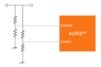
Since the EDSADC guarantees a more precise measure, out of the two measures, the one that is obtained using the EDSADC will be then used to perform the control loop to control the switches, whilst the measure that is obtained through the normal ADC is then used only for safety purposes.
DC-DC converter current sensing
The current is sensed both in primary and secondary side, to perform an accurate control loop to control the switching of the MOSFETs, but also to guarantee functional safety features to the system.
For DC current sensing in high voltage input supply rail and low voltage output supply rail, current sensor ICs can be used to get average input and output current value needed for control loops and functional safety.
Depending on the control algorithm implemented into the system fast current sensing may be required, if so, the usual current sensor ICs are not well suited due to limitation in bandwidth, so other means of current sensing are used like current transformers which are well suited for very fast current sensing.
Primary side current sensing
The current sensing in the primary circuit can be done in two ways, depending on where the current is sensed into the circuit and on the information the microcontroller needs to guarantee.
Usually, this sensing is done using a current transformer. The downside of this method is that the DC value of the current is lost, which doesn’t allow the system to recognize in this way any transformer saturation condition, in fact, in this way, only the AC value can be sensed, which is still enough to perform the control loop into the microcontroller and to sense overcurrent faults.
The current transformer also guarantees isolation from the high voltage of the primary side, allowing the microcontroller to read the current in a simple way.
To create the overcurrent detection feature using the current transformer, the AC value which is read by the microcontroller is then compared with a threshold. This concept of overcurrent detection works assuming that an overcurrent condition would cause the current value to rise very quickly, exhibiting a behavior not related to the normal working conditions.
Inductor current sensing is done placing another coupled inductor. Sensing the inductor current allows the microcontroller to monitor the zero-crossing detection and monitor the transformer saturation condition.
Most of the times current measures using current transformers are performed on AC signals whilst DC signals are not the ideal ones since it can cause the current transformer to saturate.
Adding another redundant current measure on the primary side is usually not needed since the HV battery is featured with a BMS (Battery management system) which usually performs a current sensing at its output, creating a redundant measure.
Secondary side current sensing
On the secondary side the current can be sensed in different ways depending on the control algorithm implemented into the system and on the implemented rectifier scheme.
Sensing the current on the secondary side is often regarded as challenging due to the magnitude of the current. While it is possible to utilize a 1-turn to n-turn current transformer for this purpose, it is important to note that there will be non-negligible losses associated with this approach. As a result, the current sensing typically focuses on the output DC current alone, or alternatively, a high bandwidth current sensor is employed in series with the PSFB (Phase-Shifted Full Bridge) output inductor connected to a high current busbar.
Zero crossing detection
The zero-crossing detection of the current can be very useful in the implementation of the control loop for the converter system.
This measurement can be performed both on the primary and secondary side, depending on the implementation:
Primary side:
Although there are some integrated circuits that can perform this computation on a sensed current, as of today the way it is performed is using a current-sense transformer. Being this measurement placed on the high voltage side of the system, it requires the current to be sampled in an isolated way.
Secondary side:
Getting the zero-crossing information from the secondary side allows for the measure to be much easier due to the lower voltage domain.
In this case a current sensor can be used instead of the coupled inductor.
The zero-crossing information can also be used as a source of information to perform a plausibility check with the other current sensing information that the microcontroller gets from all the other sensing means on the system, allowing for a safety feature to be implemented.
AURIX™ TC3xx fast compare comparator (FCC)
To react to an overcurrent condition in either the primary or secondary side of the converter the FCC block of the analog to digital converters is used.
The Fast Compare Comparator (FCC) is designed to achieve fast detection of input crossings against a programmable 10-bit threshold value within a very short response time (depending on analog clock frequency can reach up to 168.75 ns). Generating high-speed comparison results makes FCC useful in DC-DC converter applications for immediate PWM switch-off on over-current or voltage detection without using CPU resources, implementing what is known as “fast shut-off”.
Operating frequency selection
Choosing the optimal frequency for a system involves various trade-offs and considerations, such as functional safety, power density, size, and cost.
The operating frequency of a DC DC converter system has a significant impact as it affects the timing of the system, including fault detection and response. As the frequency increases, the magnetic components can be smaller, allowing for reduced distances and increased power density. However, this can also pose some problems for functional safety, as it can increase the risk of malfunctions.
Not only do magnetic components, such as transformers, benefit from higher frequencies, but inductors and capacitors as well. Smaller components can lead to reduced volumes, masses, and costs, while improving efficiency and precision in control. However, higher frequencies also result in increased losses in the winding, which must be considered when determining the optimal frequency for a given transformer.
In automotive applications, working frequencies are defined in specific bands due to emission regulations.
Some frequency ranges may not be available for use in certain applications. Currently, most systems operate around 100 kHz, with some newer systems operating at 200 kHz. The limiting factors for higher frequencies are typically EMI and thermal issues, as transformers become so small that they struggle to dissipate heat effectively.
To contrast the EMI issues caused by the frequency selection, Spread Spectrum techniques can be implemented, in which the frequency is deliberately spread over a wider band effectively reducing the effects of the electromagnetic interference.
Switches selection
In the context of high voltage - low voltage DC-DC converters, a careful selection of switches is crucial.
The primary side operates with SiC switches, ensuring low leakage currents and improving efficiency, while the secondary side utilizes GaN switches. It is important to note that the GaN switches on the secondary side lack a body diode, requiring a precise turn-on process to maintain system efficiency. Therefore, the implementation of an accurate control loop and precise driving capability is essential for achieving an efficient converter.
Operational amplifiers usage
A lot of the voltage and current measures in the system, used by the control loop and to guarantee functional safety functionalities, use operational amplifiers to provide the converters of the microcontroller with a value that would use at best the full range available in the analog to digital converters.
A nice way to avoid common cause failures is to use operational amplifiers there are physically separated, and not using integrated circuits that contain multiple instances of operational amplifiers on the same chip.
HV ASIL rated Gate Drivers and Voltage sensing
In the context of evolving automotive technologies, there is a potential future scenario where the low-voltage (LV) battery might be removed from the vehicle, leading to the need for the high-voltage to low-voltage (HV-LV) DC-DC converter to be rated for Automotive Safety Integrity Level (ASIL) compliance. In such a scenario, the selection of an ASIL compliant gate driver becomes imperative to ensure the continued safety and reliability of the HV-LV DC-DC converter.
Considering this prospective shift in automotive design and safety standards, it becomes essential to explore the functional safety capabilities of gate drivers, particularly in the context of the EiceDRIVER™ 1EDI3033AS, which offers advanced safety features.
The 1EDI3033AS is a single channel isolated SiC-MOSFET driver. It includes redundant DESAT and OCP protection, gate and output stage monitoring, shoot-through protection, primary/secondary supply monitoring, and internal supervision, which are crucial for ensuring the safe and reliable operation of the converter.
The gate driver features reinforced insulation, ensuring a high level of electrical isolation for enhanced safety. It also integrates an ADC for DC-link measurements and detailed error diagnosis via PWM signal, allowing comprehensive monitoring and control of the system operations.
Figure 17. EiceDRIVER™ 1EDI3033AS general representation
The internal ADC of the 1EDI3033AS gate driver can be utilized to measure an external voltage, providing a convenient means for monitoring and controlling the operation of the HV-LV DC-DC converter in an isolated way. This ADC functionality enables accurate and precise measurements of the DC link voltage, contributing to the overall performance and safety of the system.
This isolated Analog to digital converter allows to measure an analog voltage in the HV domain, reporting it in the low voltage domain using the isolated pins of the gate driver.
This specific functionality allows to replace the voltage measurement in the primary side of the converter which represents a sensible reduction in system BOM and complexity. This is because the primary side voltage sensing requires an external modulator coupled with an isolation logic integrated circuit, all powered by a dedicated power supply.
The integrated ADC can also be used to measure the temperature on the High voltage domain, removing the needs for an external temperature sensor.
Figure 18. EiceDRIVER™ 1EDI3033AS high voltage side ADC possible use cases
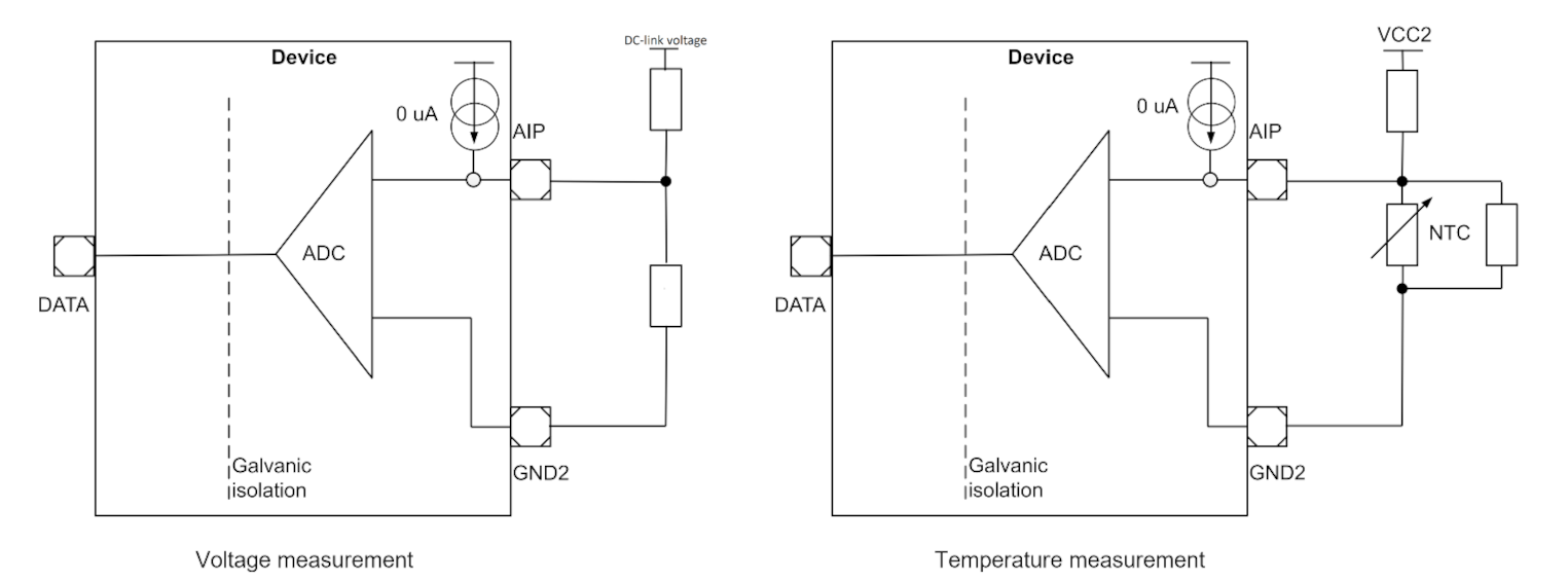
Considering that the primary side of the converter needs four different gate drivers to drive the four switches, the available ADCs that measure voltages and temperatures in the high voltage domain would be four as well, allowing for further redundance to be implemented in the voltage and temperature measurements.
The ADC block itself is not ASIL rated which means it does not have a safety concept. The argumentation for the safety use case is to provide the failure modes and fit rate related to the incorrect ADC measurement, even if the functional block itself is QM rated.
Future trends – Highly available systems and multiphase converters
In the future the 800 V battery could be divided into two 400V batteries, meaning that the DCDC converter will be duplicated, getting two outputs at 12 V each, allowing to use this converter not only to charge the 12 V battery but also to power brake by wire and steer by wire systems.
Having the two 400 V batteries will allow the system to keep running even if one of the batteries is not working, providing a limited functionality.
In Multiphase converters the Phase shift full bridge will be still used as the reference topology but implementing a multiphase architecture which can deliver power even if one of the two DC DC converters fails, effectively converting with just one of the two phases and delivering just half the power to the load. This allows systems previously mentioned, like brake by wire and steer by wire, to work even if a failure in one of the converters happens.
References
Infineon Technologies AG:
AURIX™ TC3xx User’s Manual V2.0.0
; 81726 Munich; 2021-02; Available online
Kilian, P.; Köhler, A.; Van Bergen, P.; Gebauer, C.; Pfeufer, B.; Koller, O.; Bertsche, B.:
Principle Guidelines for Safe Power Supply Systems Development
; IEEE Access, vol, 9, pp 107751_107766; 2021; Accessed: March. 11, 2024; doi: 10.1109/ACCESS.2021.3100711; Available online
Infineon Technologies AG:
AN1000 - FuSa in a Nutshell
- release note
; Available online
Glossary
Definition | Description | Notes |
|---|---|---|
ASIL | Automotive Safety Integrity Level; refer to ISO 26262-1:2018, 3.6 | |
FTTI | Fault Tolerant Time Interval | |
HW | Hardware | |
IC | Integrated Circuit | |
ISO | International Organization for Standardization | |
MCU | Microcontroller unit | |
PMIC | Power Management ICs (PMICs) | |
PSPR | Program Scratch Pad RAM | |
Safety Measure | Activity or technical solution to prevent, detect, control or mitigate systematic and random failures. | |
SW | Software | |
STP | Shoot-Through Protection: Protection typical of an inverter gate driver so that the high side and the low side of the three-phase motor legs cannot be activated simultaneously |
Revision history
Document revision | Date | Description of changes |
|---|---|---|
V1.0 | 2024-09-12 | Initial release |
V1.1 | 2024-11-11 | Minor wording change, figures resize and specific timing update |
V1.2 | 2025-05-26 | Template updated; no content update. |