AN239774 Selecting and configuring memories for power and performance in PSOC™ Edge MCU
About this document
Scope and purpose
This application note describes the internal and external memory features of the
PSOC™ Edge
MCU. The purpose of this application note is to equip developers with the knowledge and guidance required to configure the on-chip and external memories of the PSOC™ Edge MCU. By addressing the nuances of memory utilization, power consumption, and memory layout, this document aims to empower hardware and software developers to make informed decisions that optimize the power and performance of their applications. Furthermore, the inclusion of hands-on exercises serves to provide practical experience to leverage the diverse memory options offered by the
PSOC™ Edge
MCU.
Intended audience
This application note is tailored for hardware and software developers, engineers, and system architects who are involved in the design, development, and optimization of embedded systems using the
PSOC™ Edge
MCU. It is also suitable for anyone seeking a comprehensive understanding of memory utilization and its impact on power and performance in embedded applications.
Software version
3.6 or above
Target devices
PSOC™ Edge
E8x2, E8x3, E8x5, E8x6 MCUs
Introduction
The
PSOC™ Edge
MCU provides a diverse range of internal and external memories. This application note offers comprehensive insights into each of these memory types. It delves into configuring on-chip and external memories to attain the desired power and performance levels, covering aspects such as memory architecture, bus architecture, and memory access. Additionally, it explores the impact of memory on power consumption, power domains, associated memories, linker script, and memory layout, and includes practical hands-on exercises for running code from different internal and external memories.
Figure 1.
PSOC™ Edge
memory architecture
PSOC™ Edge architecture
The
PSOC™ Edge
MCU features two CPU subsystems, the Arm® Cortex® M33 running up to 200 MHz and the Arm® Cortex® M55 running up to 400 MHz. These CPUs are equipped with caches to improve performance and reduce power consumption when accessing memory. The MCU contains two SRAM sections of 512 KB each in the low-power domain. The MCU also has 5120 KB of System SRAM (SoCMEM) in the high-performance domain. The 512 KB of RRAM serves as a nonvolatile storage option primarily for code and can also be used to store certain data in the low-power domain. The overall performance of the CM55 core is enhanced by tightly coupled memory for data and instruction of 256 KB each.
For memory expansion, the
PSOC™ Edge
MCU supports the expansion of code and data memory off-chip through a Serial Memory Interface (SMIF) which enables Execute in Place (XIP) capability with external memory and facilitates the physical interface for memory expansion for external RAM and flash. The contents of the external memory can be encrypted and decrypted on the fly, enhancing the system's security. The following sections of this application note describe these internal and external memories and how to utilize them effectively.
Power domains
The
PSOC™ Edge
features two power domains, the always-on low-power domain (PD0) and the high-performance domain (PD1) as shown in
Figure 1
. Both domains are powered by the internal buck output. Both PD1 and PD0 domains operate at the same voltage. Additionally, PD1 can be independently turned off, while PD0 remains on unless the chip power is removed. For applications that do not require high-performance peripherals in the PD1 domain, the domain can be completely turned off to conserve power and brought up again as needed. See the
Summary
section for memory and associated power domain information.
Internal memories
RRAM (NVM)
RRAM is a form of embedded nonvolatile memory (NVM), where the stored information is coded in the changeable resistances of the individual RRAM elements. It behaves like a (slow) RAM with retention, independent bit toggling, and easy to handle in software. RRAM is typically used to store CPU instructions and data when the device power is off. It offers high bulk program performance and supports ultra-low-power operation. Electrically erasable programmable read-only memory and OTP regions can also be emulated in RRAM.
The RRAM in the
PSOC™ Edge
MCU is divided into two main regions:
Nonvolatile memory (NVM)
One-time programmable (OTP)
The NVM region is further subdivided into two sub-regions:
MAIN NVM (user programmable and extended BOOT)
PROTECTED NVM (only accessible by Secured Enclave)
The MAIN NVM region is user-programmable and contains an extended BOOT area, whereas the PROTECTED NVM region is only accessible by the Secured Enclave, providing an additional layer of security. See the
PSOC™ Edge
MCU datasheet for the actual size of the NVM and OTP region.
SRAM
In the PD0 domain, two 512 KB arrays (SRAM0 and SRAM1) reside in a contiguous address range. Each array has eight partitions, allowing a minimum of 64 KB for retention purposes, to enable applications to balance Deep Sleep leakage current with the amount of memory retained. The SRAM is designed in two independent blocks to facilitate simultaneous access from different processors to different regions.
System SRAM (SoCMEM)
System SRAM is also referred to as System-On-Chip Memory (SoCMEM). System SRAM is a multiported on-chip memory controller. It has multiple banks to increase overall system memory bandwidth. It contains multiple ports to allow connections to multiple buses without relying on system interconnect (bus infrastructure). Each port is connected to each memory bank via an internal bus, and each port can be either asynchronous or synchronous to the memory controller. PSOC™ Edge MCU SoCMEM is organized into 10 partitions each with four banks for interleaved access for a total of 5120 KB. This granularity allows the minimum retention partition to be 512 KB for the minimum retention current. It can be accessed from either the CM55 or the CM33, with bus arbitration.
Cache memories
Cache stores frequently accessed data in a high-speed, volatile memory to make it quicker to access than the slower main memory or storage. Its main goal is to enhance the system's performance by offering faster access to frequently used instructions and data.
ICACHE manages read transactions only and does not manage write transactions while DCACHE efficiently manages both read and write transactions for data.
Instruction cache
The instruction cache (ICACHE) aims to cache instruction fetches or instruction memory loads, coming from the processor from both internal and external memories. ICACHE has a 128-bit prefetch buffer for quick refill in the event of a cache miss.
CM33:
It has a 16 KB 4-way set associative instruction cache on the C-AHB bus.
CM55:
It has a 32 KB 4-way set associative instruction cache on the M-AXI bus.
Data cache
CM33:
Not available.
CM55:
The processor features a 32 KB 4-way set associative data cache connected to the M-AXI bus. This cache supports various inner memory attributes and allocation hints for Non-shareable memory. These attributes include Write-Back and Write-Through Cache-able, as well as Read-Allocate and No Read-Allocate options. Additionally, Write-Allocate and No Write-Allocate, along with Transient and Non-transient attributes, are also supported.
The share-ability attribute forces the region to be treated as non-cache-able, regardless of the inner memory attributes. This enables maintaining coherency at the system level. You can configure these memory attributes in the start-up code by using the MPU configuration.
Tightly coupled memories for CM55
The CM55 processor integrates instruction tightly coupled memory (ITCM) and data tightly coupled memory (DTCM), ensuring rapid and predictable access to program instructions (256 KB) and data (256 KB). Its close proximity to the CPU core reduces memory access latency, allowing for quick fetching and execution of instructions and data.
DTCM
Data tightly coupled memory (DTCM) closely integrates with the CM55 core processor, providing a specialized memory size of 256 KB for storing critical data that requires fast and deterministic access. DTCM instructions do not pass through the cache and do not impose any restriction on wait states.
DTCM is used mainly for storing data that require low-latency access, real-time processing, or data that needs to be accessed frequently. DTCM, like ITCM, is located physically close to the CPU core, separate from the system SRAM (SoCMEM), and SRAM. This reduces memory access latency and ensures that data can be read or written quickly. Access to DTCM is deterministic, ensuring consistent and predictable memory access times. This is crucial for real-time applications where timing is critical.
ITCM
ITCM stores program instructions requiring low latency and minimal contention for access, often housing critical parts of the program like interrupt service routines (ISRs), time-critical control loops, or frequently used functions. ITCM instructions do not pass through the cache and do not impose any restriction on wait states. This allows for direct and deterministic access to instructions from this TCM, improving execution speed for critical, or time-sensitive code. Accessing instructions from ITCM typically incurs zero wait states compared to accessing instructions from slower memory regions like flash memory. This reduction in wait states enhances the real-time performance and responsiveness of the MCU.
Serial Memory Interface (SMIF)
This product line has one or two SMIF interfaces (SMIF0 and SMIF1), depending on package (see the device datasheet for pins and package information). Each interface can address up to 64 MB externally, for a total of 128 MB. The SMIF allows code XIP from the external memory; it is not required to copy code into the internal memory to execute it. On-the-fly (OTF) encryption and decryption are supported.
The Serial Memory Interface (SMIF) provides a low pin count connection to off-chip (single/dual/quad/dual-quad/octal) SPI devices, such as EEPROM, F-RAM, MRAM, or NOR memories, in SDR or DDR mode, and HYPERBUS™ devices such as HYPERFLASH™ (NOR flash) and HYPERRAM™ PSRAM (Pseudo-static RAM). SMIF provides two modes for data transfer operation to and from external devices:
Execute in Place (XIP) mode:
The read and write transfers on the XIP AXI interface are translated on the fly to external device SPI transfers. The XIP mode of operation maps the external memory space to a range of addresses in the
PSOC™ Edge
MCU's address space. When this address range is accessed, the hardware automatically generates the commands required to initiate the associated transfer from the external memory. The typical use case for the XIP mode is to execute code placed in external memory directly from the CPU.
MMIO (Memory-mapped I/O) mode:
This mode supports MMIO-based access to external devices. The MMIO operation mode is less efficient than the XIP operation mode for read and write operations. However, it is more flexible than the XIP operation mode and this helps to implement other device operations in addition to read and write operations, such as programming and changing power modes.
PSOC™ Edge external memory options
Memory device | I/O signals (# denotes active low) |
|---|---|
Single SPI memory | SCK, CS#, SI, SO. This memory device has two data signals (SI and SO). |
Dual SPI memory | SCK, CS#, IO0, IO1. This memory device has two data signals (IO0 and IO1). |
Quad SPI memory | SCK, CS#, IO0, IO1, IO2, IO3. This memory device has four data signals (IO0, IO1, IO2, IO3). |
Octal SPI memory | SCK, CS#, IO0, IO1, IO2, IO3, IO4, IO5, IO6, IO7. This memory device has eight data signals (IO0, IO1, IO2, IO3, IO4, IO5, IO6, IO7) |
Some memory ICs might not support Read While Write (RWW) operations. This limitation means that any ongoing write or erase operation to the external memory connected via SMIF will block read access to the same memory. Consequently, executing code from SMIF while a write/erase operation is in progress will result in a system fault.
Recommendations to mitigate this issue are as follows:
Relocate critical code to internal SRAM or SoC memory to avoid dependency on SMIF during write/erase operations. See section
Placing code and data in a specific memory region using default linker files
for details
Avoid XIP execution for critical routines that may overlap with SMIF write/erase operations
Implement core synchronization mechanisms:
Suspend CM55 execution when CM33 is performing SMIF write/erase
Suspend CM33 execution when CM55 is performing SMIF write/erase
Use inter-core communication protocols for coordination
When performing Firmware Updates, ensure the update code is relocated to SRAM before execution
Associated code examples
PSOC™ Edge MCU: Serial flash read and write
This code example demonstrates how to interface an external QSPI NOR flash memory with the PSOC™ Edge MCU using the serial flash library. In addition, this code example readme covers how to use the Serial Flash Discoverable Parameters (SFDP) standard, which allows for the autodiscovery of flash parameters, as well as the commands for read, program, and erase operations.
PSOC™ Edge MCU: PSRAM read and write in Execute in Place (XIP) mode
This code example demonstrates how to interface with an external PSRAM using Octal-SPI DDR mode using Serial Memory Interface (SMIF) PDL in PSOC™ Edge MCU. It also demonstrates how to perform read and write operations while in XIP mode. This example writes 64 bytes of data to the PSRAM memory after entering XIP mode. The written data is read back to check its integrity. The UART resource outputs the debug information to a terminal window.
PSOC™ Edge external memory configuration
The Quad Serial Peripheral Interface (QSPI) Configurator is part of a collection of tools included in the ModusToolbox™ software. Use the QSPI Configurator to open or create configuration files, configure memory slots, and generate code for your application. The QSPI Configurator is a stand-alone tool. You can run the QSPI Configurator and use it with a ModusToolbox™ IDE application. You can also run it independently of the IDE. Then, you can either use the generated source with a ModusToolbox™ IDE application or use it in any software environment you choose.
Summary
The table provides an overview of the various memory types available in the
PSOC™ Edge
MCU, their respective use cases, and the associated power domains.
Memory | Size | Power domain | Description |
|---|---|---|---|
SRAM 0/SRAM 1 | 512 KB/512 KB | PD0 | SRAM memory is used for storing data, variables, and buffers required for runtime operations. The MCU can read, write, and manipulate data during program execution. |
RRAM | up to 512 KB | PD0 | RRAM is typically used to store CPU instructions and data when the device power is off. It offers high-bulk program performance and supports ultra-low-power operation. |
CM33 Instruction Cache | 16 KB | PD0 | To improve the execution speed and efficiency of the MCU by storing frequently accessed program instructions in a small, high-speed memory close to the CPU core. |
System SRAM (SoCMEM) | 5120 KB | PD1 | System SRAM in the PD1 domain is used for storing data, variables, and buffers required for runtime operations. |
ITCM | 256 KB | PD1 | This can be utilized for implementing essential routines like interrupt handling or real-time tasks, guaranteeing maximum responsiveness without any cache latency. |
DTCM | 256 KB | PD1 | To achieve faster, predictable, and deterministic data access, the CPU core is directly linked to DTCM for storing critical buffers and efficiently managing context-switching data in systems with rapid context switching. |
CM55 Instruction Cache | 32 KB | PD1 | To improve the execution speed and efficiency |
CM55 Data Cache | 32 KB | PD1 | Faster data access with reduced latency. |
SMIF Core 0/Core 1 | 64 MB/64 MB | PD1 | Expanding the external storage for the MCU program and data. |
Bus architecture and memory access
The bus infrastructure in a system on chip (SoC) forms the backbone of communication between various components within the chip. It is a network of buses that connect different IP blocks, such as processors, memory, peripherals, and accelerators. The bus infrastructure provides a standardized interface for data and control signals, enabling seamless interaction and data exchange among these components. It typically comprises different types of buses, such as system buses, interconnects, and peripheral buses, each serving a specific purpose. System buses and interconnects, such as the advanced high-performance bus (AHB) or advanced eXtensible interface (AXI), facilitate high-bandwidth communication between processors, memory, and other critical components.
Figure 2.
PSOC™ Edge
bus architecture
The
PSOC™ Edge
MCU family features two subsystems, SYSCPUSS and APPCPUSS, which consist of AHB5 and AXI4-based bus infrastructure that interconnects multiple bus masters with slaves. These bus interconnects use bridges, upsizers, and downsizers to connect to other interconnects of varying bus widths, allowing access from multiple masters to slaves and enabling concurrent access and efficient operation even when several high-speed peripherals are working at the same time.
Understanding bus architecture
The system uses a unified memory address space. Except for CM55’s ITCM/DTCM, all masters (CPUs, AXI/AHB DMA) see all memory structures and peripherals at the same memory locations. The software maintains the coherency of caches and I/D TCMs of each CPU or during protection context (PC) switches. For CM33, all accessible address spaces in RRAM are cacheable. Except for aliasing on SRAM/SoCMEM/Ext FLASH regions, no other area is cached. For CM55, through its M-AXI bus, all FLASH/RRAM and SoCMEM address spaces are cacheable in I/D Caches, subject to the CPU’s MPU/Secure MPU control. The CPU’s private I/D TCM memory space is noncacheable.
SYSCPUSS AHB5 interconnect
The SYSCPUSS (CM33 CPU) uses a 128-bit and 32-bit multilayer AHB5 bus matrix interconnect. The AHB5 bus masters may reside in the SYSCPUSS or outside of the SYSCPUSS (the SYSCPUSS external bus masters). Similarly, the AHB5 bus slaves may reside inside the SYSCPUSS (for example, the on-chip memory controllers) or outside of the SYSCPUSS (for example, slaves connected to the peripheral interconnect (PERI) or to the external slave interfaces). The SYSCPUSS AHB5 bus matrix interconnects the following masters and slaves:
Masters
Cortex® M33 code AHB (C-AHB) bus via instruction cache (ICACHE)
Cortex® M33 slave AHB (S-AHB) bus
Neural network lite (NNLite)
Secured Enclave
Crypto
APPCPUSS_SYSCPUSS_MS: APPCPUSS master interface from the APPCPUSS AHB5 interconnect through AHB5-to-AHB5 bridge
Debug controller (SYS-AP)
One DMA-DW controller (DMA1)
Two secure digital high capacity host controllers (SDHC0, SDHC1)
High-speed USB (USBHS) controller
Slaves
One 128-bit slave interface to system-on-chip memory (SoCMEM)
One 32-bit slave interface to SoCMEM
RRAM (NVM) controller inside SYSCPUSS
SYSCPUSS_APPCPUSS_SL: APPCPUSS slave interface to the APPCPUSS AHB5 interconnect through AHB5-to-AHB5 bridge
Two SRAM controllers (SRAMC0, SRAMC1) inside SYSCPUSS
CM33 to peripheral interconnect (PERI_CM33)
One AHB DMA to peripheral interconnect (PERI_DMA)
Serial Memory Interface port 0 and 1 (SMIF port 0, SMIF port 1)
Figure 3.
PSOC™ Edge
AHB5 bus matrix
In cases where the same master bus needs to be used by two different slave buses, the master bus can only handle one transfer at a time. As a result, a method is needed to determine which device gets to use the bus. In a multiple-bus system, "arbitration" is the process through which the system uses the shared buses. It is a mechanism for resolving conflicts when multiple devices or components compete for access to the bus to communicate with other devices or the central processing unit (CPU). Essentially, arbitration regulates the shared buses and manages the contention for bus access among various devices and components. The
PSOC™ Edge
bus matrix actively manages access arbitration between masters. An internal arbiter resolves conflicts and manages bus concurrency among masters on the bus. The SYSCPUSS uses a round-robin with latency scheme to implement bus arbitration in the AHB5 interconnect.
Figure 3
shows the SYSCPUSS AHB5 bus matrix interconnect.
AHB5 bus matrix interconnect
Cortex® M33 C-AHB bus
This bus connects the Cortex® M33 core to the bus matrix through the instruction cache. This bus is used for instruction fetch and data access to the internal and external memories mapped in the code region. The targets of this bus are the RRAM (NVM), internal SRAMs, SoCMEM, and external SMIFs.
Cortex® M33 S-AHB bus
This bus connects the Cortex® M33 core to the bus matrix. The core uses this bus to access data located in a peripheral or SRAM area. The targets of this bus are the aliased RRAM (NVM), internal SRAMs, SoCMEM, external SMIFs, and peripherals connected via PERI_CM33.
APPCPUSS AXI4/AHB5 interconnects
The APPCPUSS uses the 64-bit AXI4 infrastructure for on-chip memory and off-chip memory and devices. It employs a 32-bit multilayer AHB5 bus matrix with bridges (within APPCPUSS) as well as connect to the AHB5 bus matrix of the SYSCPUSS. The APPCPUSS AXI4/AHB5 bus matrix interconnects following masters and slaves:
Masters
Cortex® M55 64-bit master AXI4 interface (M-AXI) with associated I&D-cache
One AXI DMA controller (AXI_DMAC1/HPDMA)
U55 neural processing unit subsystem (U55 NPUSS) port 0 & 1
Graphics subsystem (GFXSS) port 2 & 3
Cortex® M55 32-bit peripheral AHB interface (P-AHB)
Two SDHC controllers (SDHC0, SDHC1)
USBHS controller
SYSCPUSS_APPCPUSS_MS: SYSCPUSS master interface from the SYSCPUSS AHB5 interconnect through AHB5-to-AHB5 bridge
PERI interface accessing ITCM and DTCM over aliased address via Cortex® M55 64-bit slave AHB5 interface
Slaves
Three dedicated AXI4 slave ports for SoCMEM
SMIF port 0 & 1
APPCPUSS_SYSCPUSS_SL: SYSCPUSS slave interface to the SYSCPUSS AHB5 interconnect through AHB5-to-AHB5 bridge
CM55 to peripheral interconnect (PERI_CM55)
One AXI DMA to peripheral interconnect (PERI_AXI_DMA)
CM55 ITCM
CM55 DTCM
Figure 4.
PSOC™ Edge
AXI4/AHB5 bus matrix
Cortex® M55 M-AXI
The Cortex® M55 CPU uses the 64-bit master AXI4 (M-AXI) bus for on or off-chip higher-latency memory and peripherals that support native AXI transactions. Except for the address space covered by ITCM, DTCM, P-AHB, and private peripheral bus (PPB), the CM55 CPU can access memory regions such as RRAM, SoCMEM, SMIF, and others over the M-AXI interface. These accessible address spaces are cacheable in I&D caches subject to the CPU’s MPU/Secure MPU control. Instruction and data access are always allowed over M-AXI. The M-AXI bus supports a store buffer (STB), which merges transactions into a 64-bit aligned double-word.
Cortex® M55 TCM buses
The 4x32-bit ITCM bus is used by the Cortex® M55 CPU for fetching instructions and accessing data from the ITCM, and the 4x32-bit DTCM bus is used for accessing data in the DTCM. The DTCM bus allows load/load and load/store instruction pairs to be dual-issued on the DTCM memory. It can also fetch instructions. The DTCM and ITCM are accessed by CM55 at CPU clock speed, with zero wait states.
Cortex® M55 S-AHB bus
The Cortex® M55 CPU has a 64-bit AHB5 slave interface (S-AHB, with width converter connected to PERI), which gives the rest of the system backdoor access to ITCM and DTCM. The system DMA can use this interface to preload/initialize ITCM and DTCM. Bus masters can access the ITCM and DTCM memories via this interface over ITCM and DTCM aliasing addresses.
Cortex® M55 P-AHB bus
The Cortex® M55 CPU uses the 32-bit peripheral AHB (P-AHB) bus to access peripherals supporting native AHB transactions.
Cortex® M55 D-AHB bus
The Cortex® M55 CPU has the debug AHB5 (D-AHB) interface with Secure Debug Control signals connected to the common debug infrastructure.
Memory aliasing
Memory aliasing allows the CM33 C-AHB bus (ICACHE) to access system SRAMs or external SMIFs. CM33 S-AHB bus uses the aliased address path and writes into RRAM (in C-AHB bus address space). Data can be read from the RRAM aliased address, but it is not preferred because it is not cached by the CM33's ICACHE. The aliasing address only applies to the CM33 processor when accessing SRAM, SoCMEM, and external flash via a code bus to facilitate code execution out of these memories. Otherwise, these devices, along with the rest, are accessed by the CM55 processor through their globally defined memory addresses. See the
PSOC™ Edge
MCU architecture reference manual for more details.
Description | Global default address | Aliasing | Size | ||
|---|---|---|---|---|---|
Non secure | Secure | Non secure | Secure | ||
RRAM (NVM) | 0x0200 0000 | 0x1200 0000 | 0x2200 0000 | 0x3200 0000 | 0x0008 0000 |
SRAM0/SRAM1 512 KB/512 KB | 0x2400 0000 | 0x3400 0000 | 0x0400 0000 | 0x1400 0000 | 0x0010 0000 |
System SRAM (SoCMEM) 5120 KB | 0x2600 0000 | 0x3600 0000 | 0x0600 0000 | 0x1600 0000 | 0x0050 0000 |
CM55 ITCM 256 KB | 0x0000 0000 | 0x1000 0000 | Reserved | Reserved | 0x0004 0000 |
CM55 DTCM 256 KB | 0x2000 0000 | 0x3000 0000 | Reserved | Reserved | 0x0004 0000 |
XIP SMIF Core 0 64 MB | 0x6000 0000 | 0x7000 0000 | 0x0800 0000 | 0x1800 0000 | 0x0400 0000 |
XIP SMIF Core 1 64 MB | 0x6400 0000 | 0x7400 0000 | Reserved | Reserved | 0x0400 0000 |
Memory wait states
When accessing a memory area from the CPU, specifically the CM33 or CM55 cores, the primary focus is on the time required to retrieve data (read) at the relevant system operating frequencies. While write access times are also relevant, writes are typically posted, allowing the operation to proceed without immediate acknowledgment. In contrast, reads must traverse the full outbound address and control signal path, as well as the inbound data access path, which directly impacts system performance and response times.
This analysis is limited to scenarios where the CPU acts as the bus master. Other potential bus masters in the system are not considered in this context.
Generally, memory access time consists of two main components:
Wait states of the memories being read
Delay through the network interconnect (NIC)
Wait states (WS) : This section focuses on wait states for RRAM and SRAM, which are of primary interest to users.
RRAM :
RRAM writes are significantly slower than RRAM reads (as is typical for most non-volatile memory) and are not considered in this context
RRAM reads are controlled by an internal 160 MHz read state machine clock, designed to produce data within 30 ns (also referred to as the "analog read time") regardless of the voltage mode (0.7 to 0.9 V)
In addition to the 30 ns analog read time, the following times are required for an RRAM read:
1 clock cycle for address read
1 clock cycle for ECC correction (assuming 0 or 1-bit correction; longer times are required for greater corrections)
Wait state calculation :
Based on the 30 ns read time, the WS value for a cycle time (Tcyc) in nanoseconds is calculated as
ceil(30/Tcyc)Examples:
For an AHB clock frequency of 200 MHz (Tcyc = 5 ns), the WS value is 6
For an AHB clock frequency of 50 MHz (Tcyc = 20 ns), the WS value is 2
Voltage (V)
Frequency (MHz)
Wait states (WS)
0.9 (HP mode)
200
6
0.8 (LP mode)
80
3
0.7 (ULP mode)
50
2
SRAM :
All SRAMs are designed to operate with zero wait states at their peak target frequencies
This means that the address is latched on one clock edge, and the data is available on the next clock edge
Access cycles remain unaffected by voltage and frequency scaling. As long as the voltage and frequency limits are observed, all SRAM wait states remain at zero
Consequently, the number of cycles required to access SRAM (via
CLK_HF0
) and System SRAM (via
CLK_HF2
) does not change under normal operating conditions
Delay through the Network Inter-Connect (NIC)
:
Table 3.
CM33 CPU
Memory resource
Outbound clock cycles
Access time
Inbound clock cycles
Comment
RRAM
3 AHB clocks
Ceil(30 ns/AHB Tcyc)
2 AHB clocks
128-bit C-AHB. I-cache refill. 32-bit access is similar
SRAM
-
-
1 AHB clock
No wait states
System SRAM
3 AHB clocks
6 system SRAM clocks
2 AHB clocks
32-bit access and 128-bit access (parallel bank read)
Table 4.
CM55 CPU
Memory resource
Outbound clock cycles
Access time
Inbound clock cycles
Comment
RRAM
3 AXI + 5 AHB cycles
2 * Ceil(30 ns/AHB Tcyc)
4 AHB + 4 AXI cycles
64-bit word read takes 2 cycles
SRAM
3 AXI clocks + 3 AHB clocks
4 AHB cycles (2 accesses)
7 AXI clocks + 3 AHB clocks
64-bit word read takes 2 cycles
System SRAM
3 AXI clocks
6 system SRAM clocks
2 AXI clocks
The first word access takes one clock cycle, and each subsequent access requires one system SRAM clock cycle
Cache and its influence on power consumption
In addition of other forms of memory, cache is a specialized form of quick-access memory with each core of a processor. It is specifically designed to speed up the transfer of instructions and data between the processor core and the memory, therefore helping bridge the access speed gap between the processor and memory. The primary purpose of cache is to improve the overall performance of the system by providing faster access to frequently used data and instructions.
Usage of cache memories can significantly improve the system performance. When caching is disabled, the data will need to be fetched directly from the memory and there will be a throughput bottleneck limited by the access speed of the memory in use.
Cache memories fail to provide benefits in the following situations:
data blocks lack cyclical patterns
prefetch algorithms cannot predict the next sequence of instructions
programs access data in a non-local non-repetitive manner, making it difficult for the cache to predict what data to store
In these cases, the cache lines are frequently replaced, resulting in a high cache miss rate, and the system consumes more power even with caching enabled, as the program fetches the needed data directly from memory, rendering the cache ineffective.
For
PSOC™ Edge
MCU, the cache configurations for CM33 core are present in the CM33 start-up code present in (
<application-directory>/bsps/TARGET_<BSP>/COMPONENT_CM33/COMPONENT_SECURE_DEVICE/s_start_pse84.c
) and cache configurations for the CM55 core are present in the CM55 start-up code present in (
<application-directory>/bsps/TARGET_<BSP>/COMPONENT_CM55/COMPONENT_NON_SECURE_DEVICE/ns_start_pse84.c
).
The default configuration for shared memories have been kept as "non-cacheable". These memories can be configured to be cacheable and then user should take care of the cache coherency mechanisms. For details on the MPU configurations, see
Understanding security configurations
.
For details on cache coherency maintenance, see
Arm® Cortex®-M55 Processor Technical Reference Manual
.
APIs to enable and disable cache
Arm® provides the routines to configure the usage of cache memory in the CMSIS library. The function definitions are present in
/mtb_shared/cmsis/<release-tag>/Core/Include/cachel1_armv7.h
. The following four functions enable and disable the instruction and data cache of the CM55 core.
/* Turns on I-Cache */
__STATIC_FORCEINLINE void SCB_EnableICache(void)

/* Turns off I-Cache */
__STATIC_FORCEINLINE void SCB_DisableICache(void)

/* Turns on D-Cache */
__STATIC_FORCEINLINE void SCB_EnableDCache(void)

/* Turns off D-Cache */
__STATIC_FORCEINLINE void SCB_DisableDCache(void)
To configure the cache for CM33 core, use the following code.
/* Disable I cache */
ICACHE0->CTL = ICACHE0->CTL & (~ICACHE_CTL_CA_EN_Msk);

/* Enable I cache */
ICACHE0->CTL = ICACHE0->CTL | (ICACHE_CTL_CA_EN_Msk);
Default memory configuration
This section describes the default memory configuration and usage that comes with the Board Support Package (BSP) for the
PSOC™ Edge
device. Most of the
PSOC™ Edge
code examples utilize the same memory configuration unless the specific use case requires modification. This chapter discusses the default memory map and linker scripts provided with the
KIT_PSE84_EVAL_EPC2
BSP.
This section uses the S-AHB Secure and Non-Secure address alias when referring to the CM33 CPU application configuration, and the physical memory address when referring to the CM55 CPU. See
Memory aliasing
for details on memory address aliasing.
The Extended Boot selects and starts the first user application (the CM33 Secure project, Edge Protect Bootloader etc.,) from a fixed memory location, as defined by the boot configuration policy. User can modify the policy by provisioning the device. See
AN237849 - Getting started with
PSOC™ Edge
security
for information on provisioning and policy file.
Memory map partitioning and allocation
illustrates the default memory layout for the
PSOC™ Edge
MCU, showcasing the division of various memories for secure and non-secure processing environments for code, data, and shared regions. This section provides an explanation of the division and allocation of memory segments in the out-of-the-box memory layout available with the default BSP (
KIT_PSE84_EVAL_EPC2
). While this application note only discusses the default BSP of
PSOC™ Edge
MCU in detail, the discussion can easily be extrapolated to other BSPs like
KIT_PSE84_EVAL_EPC4
and
KIT_PSE84_AI
. The memory map assumes a three project structure: CM33 S, CM33 NS, and CM55.
Figure 5.
Default memory map for KIT_PSE84_EVAL_EPC2 BSP
PSOC™ Edge
MCU's memory layout divides various memory segments for code, data, and shared memory sections in CM33 SPE (secure processing environment) and both CM33 and CM55 NSPE (Non-secure processing environment) domains. This default memory layout provides a specific configuration for different memory regions. See section
PSOC Edge architecture
for an overview of memories present in the
PSOC™ Edge
MCU. The below tables summarize the memory sections, region IDs, security domain classification and size for each memory section present in
PSOC™ Edge
MCU.
Region Name | Region ID | Domain | Size | Description |
|---|---|---|---|---|
Extended Boot Reserved RRAM | extended_boot_reserved | reserved | 68 KB | Region reserved for Extended Boot |
User Programmable Region | user_programmable | M33S | 296 KB | This can be utilized for various use cases like CM33 Secure Project/TF-M Image, Edge Protect Boot-loader, Internal Trusted (Secured) Storage |
User NVM Region | user_nvm | M33_M55 | 32 KB | This is a shared NVM memory region in RRAM which can be accessed by both CM33 and CM55 applications |
Unused | - | - | 28 KB | - |
Reserved Region | reserved_region | reserved | 88 KB | Reserved for secured enclave |
Region Name | Region ID | Domain | Size | Description |
|---|---|---|---|---|
Extended Boot Reserved SRAM | extended_boot_sram_reserved | reserved | 4 KB | Region reserved for Extended Boot |
CM33 Secure Shared | m33s_shared | M33S | 4 KB | Shared memory region between the CM33 secure project and the secure enclave. Secure enclave can place data in this region. |
CM33 Secure Code | m33s_code | M33S | 212 KB | Placement of instructions from the CM33 secure project |
CM33 Secure Data | m33s_data | M33S | 132 KB | Placement of data from the CM33 secure project |
CM33 Code | m33_code | M33 | 404 KB | Placement of instructions from either of the CM33 projects. |
CM33 Data | m33_data | M33_M55 | 256 KB | Placement of data from the CM33 project but also accessible to the CM55 project. |
CM33 Secure Shared | m33s_allocatable_shared | M33_M55 | 4 KB | Placement of shared code or data by CM33 secure project that can be accessed by any project. |
CM33 Shared | m33_allocatable_shared | M33_M55 | 4 KB | Placement of shared code or data by CM33 project that can be accessed by any project. |
CM55 Shared | m55_allocatable_shared | M33_M55 | 4 KB | Placement of shared code or data by CM55 project that can be accessed by any project. |
Region Name | Region ID | Domain | Size | Description |
|---|---|---|---|---|
CM55 code | m55_code_secondary | M55 | 256 KB | Allocated for the code region of the CM55 application |
CM55 Data | m55_data_secondary | M55 | 2.73 MB | This region is meant to place a data region for CM55 application, in the default case it is used to store specific buffers to be placed in System SRAM and to allocate heap for dynamic allocation of memory. |
CM33 CM55 shared | m33_m55_shared | M33_M55 | 256 KB | Shared memory between CM33 and CM55 applications. This region can be used to share data buffers among the CM33 NS and CM55 applications. This can be used for various audio, graphics, and ML use cases where applications need to share specific information or requests with each other. |
Graphics Data | gfx_mem | M33_M55 | 1.77 MB | Intended for storing dynamic GPU data for graphics use cases, such as image rendering on displays. In most use cases, this region should be used by the CM55 core or the GPU used for graphics applications. |
Region Name | Region ID | Domain | Size | Description |
|---|---|---|---|---|
CM33 secure image | m33s_nvm | M33S | 2 MB | Placement of the code from CM33 secure project |
CM33 secure trailer | m33s_trailer | M33S | 256 KB | Trailer region for CM33 secure project |
CM33 image | m33_nvm | M33 | 2 MB | Placement of the code from CM33 non-secure project |
CM33 trailer | m33_trailer | M33 | 256 KB | Trailer region for CM33 non-secure project |
CM55 image | m55_nvm | M55 | 2.75 MB | Placement of the code from CM55 project |
CM55 trailer | m55_trailer | M55 | 256 KB | Trailer region for CM55 project |
The NVM images are followed by a trailer region for each image. The trailer region is a small area at the end of each firmware slot in flash used by the bootloader to manage upgrades safely. The bootloader uses the trailer to select the image to boot, choose swap or copy for updates, control rollback, and resume safely after resets or power loss.
In addition to the above discussed memory types, there are two types of Tightly Coupled Memories (TCMs) present in the MCU. ITCM and DTCM memories can be accessed through their respective start addresses at
0x00000000
and
0x20000000
for the CM55 CPU. By default, the DTCM is utilized to hold the stack for the CM55 application. Additionally, it can be used to place custom data in the DTCM as per the application's requirements. The ITCM, on the other hand, is used to place the vector table for faster access, it is also used to place some code for execution like delay snippet and SMIF driver and syslib source files. See section
Understanding the linker script
for details.
The partitioning described in the above memory map are implemented using the default linker scripts and security settings available in the BSP. The subsequent sections in this chapter will delve deeper into linkers and security configurations for the default memory layout.
Understanding the linker script
Linker scripts are essentially configuration files that are used by the linker to specify how object files and libraries should be linked together to generate the final executable. Linker scripts are a collection of linker commands that describe how the sections in the input-compiled files should be mapped into the output executable file. They also help provide precise control over the memory configuration, output section definition, and address binding.
In this section, you will examine the linker script file for GCC. The GCC linker script file has a (.ld) extension. For complete documentation on GCC (.ld) linker script, refer to the
GCC documentation
. You can use Linker Scripts for Arm® and IAR compilers to help the linkers of the respective compilers with the linking process. These scripts function similarly to the GCC linker but with a slightly different syntax and memory region allocation philosophies.
VMA and LMA concepts
Every loadable or allocatable output section has two addresses. The first is the VMA, or virtual memory address, and the second is the LMA, or load memory address. This section discusses them and their usage.
The VMA refers to the execution address of the program — the address used by the CPU to access instructions and data while the program is running. The VMA is the address that is relevant once the system is up and running.
The LMA is the address where a section is placed in memory at the time the system is loaded. This is the address at which the program is written into memory. Generally, this is the address in a nonvolatile memory (like flash) where the program resides after being programmed into the device.
For embedded memories, the VMA and LMA may have the same value where the program is run from the exact location from where it is loaded in the memory. However, there may be cases when a section of the user application has to be loaded into a nonvolatile memory (like flash) and this section is expected to be run from a volatile memory (like RAM). This means that a start-up program must copy the section from its LMA (where it is stored in flash) to its VMA (where it should run in RAM) before the main program starts executing. In such cases, it is helpful to have two separate addresses.
Let us take an implementation example in GNU linker script to understand the concept of VMA and LMA. Consider the below linker snippet:
.examplesection : ALIGN(4)
{
    ...
    {Section Details}
    ...
} > VMA_mem_reg AT > LMA_mem_reg
> VMA_mem_reg : This specifies the Virtual Memory Address (VMA) , or the execution address. It means that when the program is running, the
.examplesectionsection will be accessed at addresses within theVMA_mem_regmemory regionAT > LMA_mem_reg : This specifies the Load Memory Address (LMA) , or the address where the
.examplesection
section is stored in the executable file. It indicates that the initial values for the
.examplesection
section are located in the
LMA_mem_reg
memory region (likely a non-volatile memory like Flash)
Therefore, the last line instructs the linker to place the
.examplesection
section into the executable file as if it were part of the
LMA_mem_reg
memory region. Then, at runtime, a startup code will copy the data from the
LMA_mem_reg
to the
VMA_mem_reg
.
Linker script for the GCC Compiler
For
PSOC™ Edge
MCU, the following linker script files are present for the GCC compiler.
COMPONENT_CORE | Linker file | Description |
|---|---|---|
COMPONENT_CM33 | pse84_ns_cm33.ld | This is the linker script file used for the CM33 non-secure project. |
pse84_s_cm33.ld | This is the linker script file used for the CM33 secure project. | |
COMPONENT_CM55 | pse84_ns_cm55.ld | This is the linker script file used for the CM55 project. |
You may customize the memory placement configurations for the described code and data regions as needed for the application. A GCC linker script file has among others two major commands: MEMORY () and SECTIONS () which are discussed in the following sections.
MEMORY command
The MEMORY command in a GNU linker script declares memory regions available in the target system. It is used to describe the size and attributes of different blocks of memory, which informs the linker how to allocate sections to specific memory regions during the linking process.
The format of the MEMORY command is as follows.
MEMORY
{
...
 region_name (attr) : ORIGIN = origin, LENGTH = len
...

}
The memory regions are specified within the 'Memory' tab of the ModusToolbox™ Device Configurator. These configurations are used to automatically generate a linker file, which is incorporated into the main linker script during the project linking process. The generated linker file is located at:
bsps/TARGET_<BSP>/config/GeneratedSource/cymem_<Toolchain>_<Core>.<Linker-Extension>
.
SECTIONS command
The SECTIONS command within a GNU GCC linker script is central to the linking process.
This directive allows you to specify exactly how sections (pieces of code or data) from the input files (usually object files, .o, and library files, .a) should be mapped into the output file (the final executable). Under the SECTIONS command, you can control the placement, alignment, and combination of these sections, among other attributes.
The output section descriptors inside SECTION command end with a [region_name] statement. This statement informs the linker about the memory region in which that output section should be placed into.
The format of the SECTIONS command is as follows.
SECTIONS
{
    /*Executable Code*/
     .text :
    {
        ...
    } [>region_name]

    /*Initialized Data*/
    .data :
    {
        ...
    } [>region_name]

    /*Uninitialized Data*/
   .bss :
    {
        ...
    } [>region_name]
}
Structure of GCC linker script
The basic structure of the GCC linker script for
PSOC™ Edge
MCU is as follows:
/* Specify the output format for the linker script */
OUTPUT_FORMAT ("elf32-littlearm", "elf32-bigarm", "elf32-littlearm")

/* Search for libraries in the current directory */
SEARCH_DIR(.)

/* Specify the group of libraries to link against */
GROUP(-lgcc -lc -lnosys)

/* Define the entry point of the program, which is the reset handler */
ENTRY(Reset_Handler)

/* Define the stack size for the application */
/* Include the device memory definitions generated by the Device Configurator */
INCLUDE cymem_gnu_CM33_0.ld

/* Device definitions */
/* Section definitions */
SECTIONS
{
    /* This section is intended to hold the main non-secure (NS)
     * application code for the Cortex-M33 */
    .app_code_main : ALIGN(VECTORS_ALIGNMENT)
    {
        ...
    } [>region_name]

    /* Exception tables and Exception Index tables for ARM architecture */
    /* Copy table and Zero table section definitions */

    /* A section for performance-sensitive or critical functions that
     * need to be executed in SRAM */
    .app_code_ram : ALIGN(4)
    {
		...
    } [>region_name(VMA)] AT [>region_name(LMA)]


    /* A section for initialized data memory */
    .data : ALIGN(4)
    {
		...
    } [>region_name(VMA)] AT [>region_name(LMA)]

    /* BSS, Heap, GPU buffer and other region definitions */

}
Linker script for other toolchains
Arm® Toolchain:
The linker script for Arm® toolchain has a
.scat
or
.sct
file extension (for “scatter”). It has no commands; instead it separately defines regions and sections only. It has a load region. The load region contains several execution regions, which in turn contain one or more section attributes. The linker script for Arm® toolchain can be found at
CM33:
bsps/TARGET_<BSP>/COMPONENT_CM33/TOOLCHAIN_ARM
CM55:
bsps/TARGET_<BSP>/COMPONENT_CM55/TOOLCHAIN_ARM
For complete documentation on Arm® (
.sct
) linker script, see
Arm® documentation
IAR Toolchain
The linker script for IAR toochain has a
.icf
file extension. It uses "define symbols" command to define the various memory and data regions and then uses the "place in" command to control what sections is placed in which memory. The linker script for IAR toolchain can be found at
CM33:
bsps/TARGET_<BSP>/COMPONENT_CM33/TOOLCHAIN_IAR
CM55:
bsps/TARGET_<BSP>/COMPONENT_CM55/TOOLCHAIN_IAR
For complete documentation on IAR (
.icf
) linker script, see
IAR documentation
LLVM_ARM Toolchain
The linker script for LLVM_ARM toolchain has a
.ld
file extension similar to the GNU linker script. The syntax for basic linker scripts is nearly identical with the GNU linker, but GNU linker script supports additional GNU-specific features, while the focus of LLVM linker script is more on compatibility and performance of the applications. The linker script for LLVM_ARM toolchain can be found at
CM33:
bsps/TARGET_<BSP>/COMPONENT_CM33/TOOLCHAIN_LLVM_ARM
CM55:
bsps/TARGET_<BSP>/COMPONENT_CM55/TOOLCHAIN_LLVM_ARM
Understanding security configurations
PSOC™ Edge device security restrictions can be configured by software for applying restrictions for accessing the various memories and peripherals. See Protection Units section in PSOC™ Edge architecture reference manual for more details. Security configurations for PSOC™ Edge MCU has two major components:
S/NS attribute on Address alias (TrustZone® SAU/IDAU configuration):
These attributes are configured using Implementation Defined Attribution Unit (IDAU) and Security Attribution Unit (SAU) configurations provided by the TrustZone® architecture. Hence, these are only applicable for the CM33 CPU. IDAU configurations are fixed for device and you can only make use of SAU configuration in secured software to implement the required attribute on address regions. SAU defines the access restrictions for a particular address region on the basis of the secure/non-secure state of CPU (secure/non-secure SW). TrustZone® blocks all access to memory region marked as secure by non-secure state of CPU (non-secure SW), whereas otherwise is allowed. For further details, see the TrustZone® section in the PSOC™ Edge architecture reference manual
System-wide access restrictions for memory and peripheral (MPC and PPC):
These attributes are configured by MPC, PPC as per Protection Context (PC) at system (bus master) level hence applicable to all bus masters. It defines the access of a particular memory region on the basis of a Secure/Non-Secure attribute and PC of bus master trying to access the memory. As per MPC configuration secure master(s) executing in a configured protection context can only access memory region marked as secure, similarly non-secure master can only access memory region marked as non-secure. If memory access tries to violate the given configuration, a fault will be generated signaling an illegal access to memory. For further details, see the TrustZone® section in the PSOC™ Edge architecture reference manual
The Infineon Device Support Library provides the following protection personalities for
PSOC™ Edge
devices:
Protection domain personality
:
The Protection Domain personality lets you set security attributes for device memory. The Device Configurator allows for 15 protection domains and the BSP configures 6 domains by default with specific access and security settings as discussed in
Table 10
. Users have the flexibility to create their own protection domains, tailoring the settings to meet the specific needs of the application.
Table 10.
Default protection domains
Domain
Name
Description
Domain 0
M33S
CM33 secure memory domain. This domain is only accessible within the Secure processing environment (SPE).
Domain 1
M33
CM33 memory domain. This domain is accessible by both the Secure processing environment (SPE) and the non-secure processing environment (NSPE)
Domain 2
M55
CM55 memory domain.
Domain 3
M33NSC
Direct calls from NSPE to SPE are prohibited. The NSC domain is used as gateway for secure SPE function access.
Domain 4
M33_M55
Shared memory domain between CM33 and CM55 applications.
Domain 5
reserved
Reserved Domain. This domain should not be assigned to user-defined memory regions. It is used internally by the Device Configurator and no code or configuration is generated for regions assigned to it
When a memory region is assigned to a domain, the region inherits all settings from that domain, including security access and configurations for the MPC, SAU, and related security components. These configurations are known as 'Protection domain parameters' and are configured in the Device Configurator.
Figure 6
shows the protection domain parameters for the Domain 0 (M33S). The parameters within the domain personality are discussed below:
'Top level protection' parameter sets the domain’s security state to one of the following:
Secure: Only Secure code can access this domain
Non-Secure: Accessible by Non-Secure code
Non-Secure Callable (NSC): Provides controlled entry points for Non-Secure code to call Secure functions
'Peripheral protection' parameter controls whether peripherals in this domain can be accessed from unprivileged (user) mode. Enable this only if unprivileged software must talk to these peripherals; otherwise leave it disabled to restrict access to privileged code
'Accessible by' parameter lists available protection contexts (PCs) for each memory domain
For each PC that you enable for a particular memory domain, you must also provide the configuration in the 'Memory Protection' parameter from among the following settings:
Read allowed: Can this PC read from the domain?
Write allowed: Can this PC write to the domain?
Secure attribute: Is this PC operating as Secure or Non-Secure for this domain’s access checks?
Figure 6.
Domain 0 Protection domain parameters
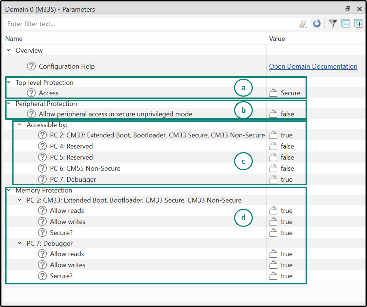
Note that the default domains are read-only and are not supposed to be modified by the users. They are designed to ensure reliable and predefined functionality. The only exception is in Custom Security mode, where you can enable or disable Debugger PC access within the M33S default domain using the checkbox in the top-level Protection resource. For any other modification requirement, a custom protection domain should be created
Memory Protection Unit (MPU) personality
:
The ARMv8-M memory protection units (MPUs) are programmable units and part of the CPU. A MPU distinguishes user and privileged accesses from a CPU. The MPUs allow privileged software to define memory access permission (R/W/X) and monitors the instruction fetch and data access operations from the CPU. In the
PSOC™ Edge
platform, the M33 CPU has eight secure MPUs and eight non-secure MPUs. The M55 CPU has eight non-secure MPUs. Any access violation observed by the MPU triggers a fault.
After enabling a MPU region, the ‘Base Address’ and ‘Size (bytes)’ should be configured. 'End address' is generated based on the Base Address and Size. Once enabled, the options for region securities are as follows: (wait for ravikiran for device-memory)
Privileged access only: When enabled, only privileged code can access this region. Unprivileged code will be blocked and result in a fault
Writable: When enabled, software can write to this region. When disabled, the region is read-only
Executable: When enabled, code can run from this region. When disabled, instruction fetches are blocked
Device memory: Mark this if the region maps to device/peripheral registers
Memory Protection Controller (MPC) personality
:
The memory protection controller (MPC) is situated on the AHB/AXI bus. The following memories are equipped with MPCs: RRAM, SRAM, System SRAM (SocMEM), and SMIF (external memory). This personality allows to configure MPC response on assess violation of the Security Domains
Peripheral Protection Controller (PPC) personality
:
PPC provides peripheral access control based on Arm® TrustZone®-M secure/non-secure (NS), Privileged/Unprivileged (P) and protection context (PC) attributes. PPC is situated between bus masters and peripherals. In the peripheral space, the PPC groups the MMIO registers of a peripheral which typically require same security permissions into "regions". The PPC checks the security attribute of a peripheral region against the transaction attribute from the masters for a security violation. If the transaction has security violation, then the transaction is blocked
Security Attribution Units (SAU) personality
:
The Security Attribution Units (SAU) personality displays the current SAU security settings for device memory. It is primarily used to configure regions within memory that are designated as ‘Non-Secure Callable’ by the protection domain associated with the memory regions.
The SAU (Security Attribution Unit) defines which parts of memory are Secure, Non-Secure Callable (NSC), or Non-Secure. By default, all memory is Secure, which means code running in the Non-Secure world cannot access it or call functions stored there. The other configurations include:
Non-Secure Callable (NSC): Mark a small region as NSC when you want Non-Secure code to call into Secure functions. NSC only allows controlled function entry points; it does not allow direct data access
Non-Secure: Mark regions as Non-Secure when Non-Secure code must run from them or read and write their data. Non-Secure code can execute, read, and modify memory in these regions
In this flow, the SAU is primarily used to define the NSC 'gateway' regions. Based on those definitions, the NSC region is identified and the remaining regions are treated as non-secure.
The SAU personality is available in Secure cores. The Device Configurator generates a file ‘
cycfg_sau.h
’ with the function
Cy_SauInit(void)
for SAU configuration. This function has to be called from the secure core
main()
function
Power and performance impact for memory accesses
The system's efficiency depends on the type of application and its memory requirements. Small-scale systems can function adequately with internal memory alone. However, larger applications, such as image processing or graphical tasks, may necessitate additional memory beyond the internal RRAM and SRAM. For such cases, off-chip SMIF memories can provide the necessary extra storage. Furthermore, encrypting and decrypting the data on the fly can enhance security when accessing the storage.
For details on low-power modes in
PSOC™ Edge
MCU devices, and power management strategies for low-power application design, see
AN237976 -
PSOC™ Edge
MCU low power modes and power reduction techniques
.
Effect of different memory types on power consumption
Application design on embedded systems involves dealing with limited memory resources and power consumption constraints. Real-world MCU-based embedded application designs usually employ a combination of both internal and external memory to strike a balance between performance and power to achieve an optimal solution for their application.
Internal memory includes on-chip memories like RRAM, SRAM, and System SRAM (SoCMEM). External memory refers to the secondary memory that is present outside the processor such as QSPI/OSPI flash. This is typically used for storing application data with a higher memory footprint.
To optimize the power to performance ratio of applications, the application developer must decide the optimal placement of data and code in the correct memory. In this section, some qualitative strategies to consider when choosing the appropriate memory as per the requirements of your application.
Internal memories reside on-chip and therefore exhibit faster read/write operations when compared with memories that reside outside the chip. However, internal memory storage is limited and for applications with high memory demanding use cases like graphics and connectivity, it might be a challenge to only rely on internal memories. For simple application designs, if the usage of internal memory is sufficient, it would provide the optimal power efficiency for the application. However, for applications which involve large code size and data to store or process, like graphics, connectivity, machine learning, the internal RRAM and/or the SRAM will not be sufficient and the external memories must be used. External memories like SPI flash provide larger memory space at the cost of speed and power efficiency. It is recommended to keep an instruction cache (ICACHE) on when using external memory for data or instructions. This helps in minimizing power consumption. Application designs for lowest power and maximum performance can be achieved using internal memories. To optimize for power and performance, you may consider moving the code to the most appropriate memory locations for that particular application. Detailed steps for code and data movement across memories are covered in the section
Memory configuration use cases
.
See the following chart for a typical representative comparison of power vs performance characteristics of different memories present on the
PSOC™ Edge
MCU. Note that this is just an indicative image for qualitative analysis. The memory sizes are not to scale.
Figure 7.
Power consumption vs performance comparison
Power optimization techniques
Configuring system SRAM
: For the system Deep Sleep, put the system SRAM to Deep Sleep using the following function:
Cy_SysPm_SetSOCMEMDeepSleepMode
(
CY_SYSPM_MODE_DEEPSLEEP
)
;
For applications that do not need system SRAM, you may completely turn it off using the following function and run the code from ITCM. See
Memory configuration use cases
on how to use ITCM. Make sure the clock supplied to the system SRAM block is also disabled before calling this function using Cy_SysClk_ClkHfDisable() API.
/* Disable System SRAM (SoCMEM) */
Cy_SysEnableSOCMEM
(
false
)
;
Disabling external flash
: If your application does not have size constraints and can be completely moved to internal memories, you may disable the external flash altogether to reduce power consumption. The following API functions can be used to enable and disable the SMIF domain. Make sure the clock supplied to the SMIF block is also disabled before calling this function using Cy_SysClk_ClkHfDisable() API.
/* Disable SMIF Block
The SMIF block can be disabled only when it is not in the active state.
Use the Cy_SMIF_BusyCheck() function to check before calling the disable function.
Make sure the clock supplied to SMIF block is also disabled before calling this function using Cy_SysClk_ClkHfDisable

Parameters
base:   Holds the base address of the SMIF block registers. */

__STATIC_INLINE void Cy_SMIF_Disable( SMIF_Type* base)


/* De-Initialize SMIF block
This function de-initializes the SMIF block to default values.
The SMIF must be disabled before calling the function.

Parameters
base:   Holds the base address of the SMIF block registers. */

void Cy_SMIF_DeInit(SMIF_Type* base)
Disabling high-power domain (PD1)
: PD1 can be independently turned off, while PD0 remains on unless the chip power is removed. For applications that do not require high-performance peripherals in the PD1 domain, the domain can be completely turned off to conserve power and brought up again as needed.
The following API functions can be used to enable and disable the PD1 domain
/*Enable PD1*/
void Cy_System_EnablePD1(void);

/*Disable PD1*/
/*The System SRAM must be disabled before disabling PD1 domain using this API. */
void Cy_System_DisablePD1(void);
Configuring SRAM
: In Deep Sleep mode, retain SRAM in blocks of 64 KB. For applications that do not utilize the whole of the 1 MB SRAM, retain selective blocks via the following function:
cy_en_syspm_status_t Cy_SysPm_SetSRAMMacroPwrMode(cy_en_syspm_sram_index_t sramNum, uint32_t sramMacroNum, cy_en_syspm_sram_pwr_mode_t sramPwrMode);Optimizing core voltage and frequency
: Clock frequencies of certain memory peripherals like system SRAM and SMIF interface can be configured by the user as per requirement. You may also consider selecting the right core voltage and core clock frequencies as per different available low-power modes to optimize power consumption. See
AN237976 -
PSOC™ Edge
MCU low power modes and power reduction techniques
.
Usage of DMA
: You may also consider using the DMA for memory transactions while the processor is put to sleep to reduce system power consumption.
Performance optimization techniques
Usage of TCM memories
: For applications utilizing the CM55 core, use the tightly coupled memories (ITCM and DTCM) to achieve faster, predictable, and deterministic data access. The tightly coupled memories are physically placed close to the CM55 core and therefore the access times to these memories is much faster compared to any other internal memory
Usage of data cache
: Utilize the data caching in CM55 projects for small repetitive operations needed in the application
Utilization of application-specific coprocessor
: Utilize the U55 coprocessor to accelerate machine learning inference applications such as automatic speech recognition and keyword identification
SMIF interfacing
: When using external memory, it is optimal to utilize SPI protocols with higher speed, like Quad over Dual or Octal over Quad, and higher data rate transfer, such as Dual Data Rate (DDR) over Single Data Rate (SDR), to achieve the best performance
Compiler Flags
: User may optionally choose to apply compiler optimization flags with the goal of improving performance or reducing resource usage. Common optimization flags include "-O0", "-O1", "-Ofast", etc.
-O0 refers to 'no optimization', while -O1 through -O3 refer to progressively higher optimization levels favoring proportionate increase in the runtime execution speed of the programs.
Each compiler optimization level represents a tradeoff between compilation time, execution speed, and code size. Lower compilation flags (-O1 or -O2) are often associated with shorter compilation time with smaller memory footprint of the program and lead to higher debug clarity and deterministic control over code behavior. Higher (more aggressive) optimization levels (-O3 or -Ofast) may increase the memory footprint of the program to achieve higher execution speed. These are targeted to maximize runtime performance, reduce resource usage, or take full advantage of the hardware’s capabilities. Aggressive optimization flags are commonly used to showcase hardware or software performance in benchmarking scenarios.
There also compiler optimization flags aimed to optimize the program for size. These flags aim to reduce the size of the generated binary, making the program smaller in terms of memory footprint and disk storage. While optimizing for size can sometimes slightly impact runtime performance, it is extremely useful in scenarios where memory or storage is a constraint.
Perform the following steps to add the optimization flags to your applications:
Set CONFIG=Custom in the common.mk file
Set CFLAGS and CXXFLAGS in the Makefile for each core with the desired optimization
Memory configuration use cases
This section describes the process of connecting and running code across different types of memory, including RRAM, SRAM, and System SRAM (SoCMEM). Furthermore, it provides detailed insights into the techniques for strategically situating a block of data within different memory regions. The code example, CE238541 PSOC™ Edge MCU: Hello world, which is accessible in the ModusToolbox™, serves as the starting point for this section. It is assumed that readers possess a level of familiarity with the usage of the
PSOC™ Edge
device and EVK, along with practical experience in working with the "Hello World" code example in the ModusToolbox™. For those who have yet to explore this code example, it is recommended to commence with
AN235935-Getting started with
PSOC™ Edge
E84 on ModusToolbox™ software
.
PSOC™ Edge
code example is structured around three projects, namely proj_cm33_s, proj_cm33_ns, and proj_cm55. Throughout this chapter, the explanations are centered on CM33 secure project (proj_cm33_s), CM33 non-secure project (proj_cm33_ns) and CM55 project (proj_cm55) emphasizing that the foundational concept remains consistent across all other projects.
As observed in the section
Understanding the linker script
, the linker file establishes a default memory allocation for placing your code and data. For instance, in proj_cm33_ns, the default placement involves placing data in SRAM1 (
.data
) while the code is placed in External Flash (
.app_code_main
), and SRAM (
.app_code_ram
). However, there are situations where you may need to modify this allocation. For example, you might need to relocate a code segment to RRAM or position data in System SRAM (SoCMEM) for reasons related to power efficiency and performance, as elaborated in the section
Power and performance impact for memory accesses
. Examples in this section are demonstrated using the
KIT_PSE84_EVAL_EPC2
BSP but the methods can be extended to other
PSOC™ Edge
BSPs as well. This section describes the following:
Placing code and data in a specific memory region using default linker files
Assigning functions and variables to a linker section
Each compiler provides a mechanism to place your code and data into a memory region of your choice.
PSOC™ Edge
linker files provide the most commonly used sections in the default linker files. You can use of these sections for your application needs. Additionally, you can still create the sections on your own or customize them as needed for the use case.
In the following sections, specific examples and work towards achieving common use cases by utilizing the preexisting memory regions and sections from the default linker files are described.
Placing data in SOCMEM in the cm33_ns project:
In the cm33_ns project, the default configuration allocates data to SRAM1 using the
.data
section. If you want to allocate the data to SOCMEM instead of SRAM1, you can achieve this by utilizing CY_SECTION directed to
.cy_socmem_data
. A sample code snippet is shown for reference:
/* Place data in a specific memory section */
CY_SECTION(".cy_socmem_data") __attribute__((used)) unsigned int my_var = 0;
This method is not limited to a single variable. You can also allocate an array or structure using the same approach. You can allocate as many variables as needed, as long as they fit within the target memory region
Placing code in SRAM1 in the cm33_ns project:
In the cm33_ns project, the default configuration places code on external flash using the
.app_code_main
section. If you want to place the code on SRAM1 instead of external flash, you can achieve this by utilizing CY_SECTION directed to
.cy_sram_code
A sample code snippet is shown for reference:
/* Place code in a specific memory section */
CY_SECTION(".cy_sram_code") __attribute__((used)) int my_sram_func(void);

/********************************************************
* Function Name: my_sram_func
********************************************************/
unsigned int my_sram_func(void)
{
    /* function body here */
    return 0;
}
Placing code in the ITCM in the cm55 project:
The default configuration allocates code to the external flash using the
.app_code_main
section outlined in the cm55 linker file. However, certain specific codes like syslib and SMIF drivers are positioned in the ITCM using the
.app_code_itcm
section. If there is a need to place a particular piece of code in the ITCM, it can be achieved by utilizing CY_SECTION to allocate the code to the
'.cy_itcm'
section, sending it to the ITCM memory. See the sample source code to place the code in the ITCM section:
/* Place code in ITCM */
CY_SECTION(".cy_itcm") __attribute__((used)) unsigned int my_itcm_func(void);

/********************************************************
* Function Name: my_itcm_func
********************************************************/
unsigned int my_itcm_func(void)
{
    /* function body here */
    return 0;
}
Placing data in DTCM in the cm55 project:
In the cm55 project, the default configuration places data in DTCM using the
.data
section defined in the cm55 linker file. There is no need to make any changes to the code or linker to place data in DTCM, in the default case. Note, if you have changed the default location for data from DTCM to another memory location, use the
'.cy_dtcm'
section to place data in DTCM. Make sure
'.cy_dtcm'
is appropriately included in a memory region in the linker.
The focus so far has been on using the default memory configurations provided by the linker files. This keeps things simple: you can leverage existing sections and memory regions without needing to create custom ones or worry about security settings. However, real-world projects often require more control. The next example explores a more complex situation where the default memory map and security configurations might not be sufficient. It describes how to create a dedicated section for your specific needs and configure security settings that are not readily available. By tackling these challenges, gain a deeper understanding of how to manage memory and security aspects even when they go beyond the built-in defaults
Placing the code in RRAM:
Some use cases might necessitate storing specific code sections in RRAM for persistent data storage or other purposes, the default linker files for cm33_s, cm33_ns, and cm55 does not include a dedicated linker section explicitly labeled for RRAM. To illustrate how to handle this scenario, consider a cm33_ns project and perform the following steps.
Open the source file (for example, main.c) and create a named section as shown. This code instructs the compiler to assign a section, ".my_rram_code" to function 'my_rram_func'
/* Add a RRAM section in source file */
CY_SECTION(".my_rram_code") __attribute__((used)) unsigned int my_rram_func(unsigned char *buf);

/********************************************************
* Function Name: my_rram_func
********************************************************/
unsigned int my_rram_func(unsigned char *buf)
{
    /* function body here */
    return 0;
}
Open ModusToolbox™ Device Configurator, and select the 'Memory' tab. Under the RRAM memory section, create a new region
my_rram_region
. Select the Domain as
M33
and enter the desired offset and size as illustrated in
Figure 8
.
Figure 8.
RRAM memory placement
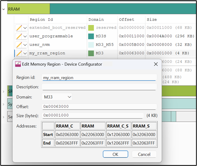
Click on 'OK' and save the file. The Device Configurator will generate the linker with the MEMORY command at
bsps/TARGET_<BSP>/config/GeneratedSource/cymem_gnu_CM33_0.ld
which will be utilized by the default linker script during the project linking process
To store the ".my_rram_code" section in the
my_rram_region
memory region and reflect it in the RRAM memory, we must instruct the linker script. The below linker script snippet should be placed in the CM33 non-secure linker file.
 /* Add a RRAM section in source file */
.app_code_rram :ALIGN(4)
{
    KEEP(*(.my_rram_code))

    . = ALIGN(4);
} > my_rram_region
Note:
The examples provided above are just a few instances. You have the flexibility to utilize these available sections and route the code and data to the memory regions that best suit your application's requirements. For example, you can place the code/data in SoCMEM, SRAM, External Flash, ITCM, and DTCM based on your application needs. The fundamental concept remains unchanged for all the scenarios.
Placing the code from a source file into a dedicated linker section
Manually assigning individual variables and functions to specific linker sections can be cumbersome when dealing with large amounts of code. While this approach works well for a small number of elements, it becomes inefficient for extensive relocation. For scenarios where you want to move all functions or data from a source file into separate sections, compilers offer a more efficient file-level management option. This allows you to handle entire code segments at once, significantly streamlining the process.
In the default linker files, you can see some code being already placed into the dedicated section. Look at the
cm33_ns linker
file. By default, the code will be placed in
.app_code_main
regions, which is in external flash. As an example, consider how to move code from a specific file into the
.app_code_ram
section in SRAM. To move the code to a specific section, remove it from its default location, which is
.app_code_main
. The following code snippet demonstrates how the
.app_code_main
section utilizes the EXCLUDE_FILE command to omit code from the cy_syslib.o, cy_syslib_ext.o, cy_smif.o, cy_smif_memslot.o, cy_smif_sfdp.o, cy_smif_hb_flash.o, and cyhal_qspi.o files.
/* Exclude the code from section */
.app_code_main : ALIGN(4)
{
    .
    .
    .
    /* Exclude certain files from this section as they will be placed in RAM */
    *(EXCLUDE_FILE(*cy_syslib.* *cy_syslib_ext.* *cy_smif.* *cy_smif_memslot.* *cy_smif_sfdp.* *cy_smif_hb_flash.* *mtb_hal_memoryspi.* *mtb_serial_memory.* *freertos/Source*.* *cy_clib_support*.* *cy_mutex_pool*.* *cy_time.* *cyabs_*.* *cy_worker_thread.* *cmsis*.*) .text*)

} > m33_nvm_sel
After removing the code from the
.app_code_main
section, relocate it to a section of your choosing. Default linker file locates the complete code from
cy_syslib
,
cy_syslib_ext
,
cy_smif etc into the
.app_code_ram
region, which is located in SRAM1 memory. The following code snippet demonstrates the syntax for placing code in a custom section:
/* A section for performance-sensitive or critical functions that need to be executed in SRAM */
.app_code_ram : ALIGN(4)
{
        .
        .
        .
	*cy_syslib_ext.*(.text*)
	*cy_syslib.*(.text*)
	*cy_smif.*(.text*)
	*cy_smif_memslot.*(.text*)
	*cy_smif_sfdp.*(.text*)
	*cy_smif_hb_flash.*(.text*)
	*mtb_hal_memoryspi.*(.text*)
	*mtb_serial_memory.*(.text*)
	*freertos/Source*.*(.text*)
	*cy_clib_support*.*(.text*)
	*cy_mutex_pool*.*(.text*)
	*cy_time.*(.text*)
	*cyabs_*.*(.text*)
	*cy_worker_thread.*(.text*)
	*cmsis*.*(.text*)

	. = ALIGN(4);
} > m33_code_sel AT > m33_nvm_sel
In this example, the linker file from the cm33_ns project is utilized. You can observe a similar implementation in both the cm33_s and cm55 projects as well. This approach can be readily extended to all other source files as required. For instance, to allocate all the code from a source file named
my_file.c
to the ITCM, do the following:
To exclude the code in
my_file.c
from the default code section that is
.app_code_main
in external flash using EXCLUDE_FILE command:
/*Excluding file from the NVM section*/
.app_code_main : ALIGN(4)
{
    .
    .
    *(EXCLUDE_FILE(*my_file.*) .text*)
    .
    .
} > m33_nvm_sel
Include these contents to
.app_code_itcm
section, which is placed in ITCM.
/* Placing code from file to ITCM */
.app_code_itcm : ALIGN(4)
{
    .
    .
    *my_file.*(.text*)
    .
    .
} > m55_code_INTERNAL AT > m55_nvm_sel
To move other types of data sections, such as
.rodata
,
.rodata.*
,
.constdata
,
.constdata.*
,
.conststring
, and
.conststring.*
, you can use a similar approach. For example, to move the
.rodata
section from
my_file
to the
.app_code_itcm
section, you can add the following statement:
.app_code_main : ALIGN(4)
{
    .
    .
    *(EXCLUDE_FILE(*my_file.*) .rodata)
    *(EXCLUDE_FILE(*my_file.*) .rodata.*)
    *(EXCLUDE_FILE(*my_file.*) .constdata)
    *(EXCLUDE_FILE(*my_file.*) .constdata.*)
    *(EXCLUDE_FILE(*my_file.*) .conststring)
    *(EXCLUDE_FILE(*my_file.*) .conststring.*)
    .
    .
} > m33_nvm_sel
Include these contents to
.app_code_itcm
section, which is placed in ITCM.
.app_code_itcm : ALIGN(4)
{
    .
    .
    *my_file.*(.text*)
    *my_file.*(.rodata*)
    *my_file.*(.rodata.*)
    *my_file.*(.constdata*)
    *my_file.*(.constdata.*)
    *my_file.*(.conststring*)
    *my_file.*(.conststring.*)
    .
    .
} > m55_code_INTERNAL AT > m55_nvm_sel
In the preceding sections, the process of allocating code to various linker sections and different memory regions is covered. While the examples primarily centered on a few memory types like ITCM, SRAM and External Flash, you can seamlessly apply these concepts to other memory types such as System SRAM(SOCMEM) and RRAM. It is important to be mindful of the memory regions defined in the default linker file when placing code or data into custom sections. The linker file specifies the available memory areas and their properties. If you intend to place code or data in a new memory region that is not predefined in the linker file, take additional steps to create those memory regions. You can see an example scenario in the
Customizing the memory MAP
section.
Customizing the memory MAP
In previous sections, how to move a part of the data and code across memory was discussed. In this section the memory map will be modified at the project level using the memory tab of ModusToolbox™ Device Configurator. For detailed instructions on using the memory tab, refer the section 'Memory tab' of the
Infineon Device Configurator User Guide
In this section, take the
PSOC™ Edge
: Hello World application as an example and learn how to customize the memory map for our example scenarios. The examples in this section are:
Customizing the existing memory layout of external flash by increasing the size for CM33 non-secure project and decreasing the size of the CM33 secure project
Placing the entire application (CM33 secure, CM33 non-secure, and CM55 projects) in RRAM and executing from RRAM
Loading the application in SRAM and executing from SRAM
Note:
If the project has already been built and you then move the
m33s_nvm
memory region, the linker may report: "start address of `.gnu.sgstubs' is different from previous link." This happens because a previously generated object (the non-secure callable veneer, nsc_veneer.o) still encodes the old addresses. In order to solve the error, you must remove the stale veneer object file (present at
<application-directory>/proj_cm33_s/nsc_veneer.o
) from the build output and perform a clean rebuild so it is regenerated with the updated memory addresses. As a general precaution, after changing memory layout you should always perform a clean build so all generated artifacts reflect the new memory map.
Modifying the existing memory layout of external flash
Default memory configuration
described the default configurations provided by the
PSOC™ Edge
BSP. This configuration is used by most of the code examples including
PSOC™ Edge
MCU: Basic Secure Application and
PSOC™ Edge
MCU: Hello world. In this section, we will customize the default memory layout of external flash by increasing the allocated size for the cm33_ns project in external flash from 2 MB to 2.5 MB. This also means that the allocated size of cm33_s project must be reduced from 2 MB to 1.5 MB.
Note:
This section demonstrates how to modify the memory layout for external flash. The same approach can be applied to adjust the memory layout for other memory regions as well.
Figure 9.
PSOC™ Edge
modified memory map
Figure 9
represent the modified memory map discussed above. See the differences with respect to the original memory layout in
Default memory configuration
. To achieve the target memory map as described, do the following:
Modify the memory layout in ModusToolbox™ Device Configurator
Update the CM33 NS project start location
Memory configuration in device configurator
There is a need to update the size and offset for memory regions. Following are the steps to change the memory layout of the external flash for the selected ModusToolbox™ project.
Launch the ModusToolbox™ Device Configurator and navigate to the 'Memory' tab. Under the device's MPN (Manufacturer Part Number), review the default memory layout configuration, which displays the various memory regions supported by the device
Notice in
Figure 10
that the external flash memory listed under
Serial Memory Interface Block 0
(SMIF0) allocates
2 MB
for the CM33 secure image (memory region
m33_s_nvm
) and
2 MB
for the CM33 non-secure image (memory region
m33_nvm
). To achieve the desired memory sizes, we will adjust the offset and size of these memory regions
Figure 10.
Default memory layout for external flash
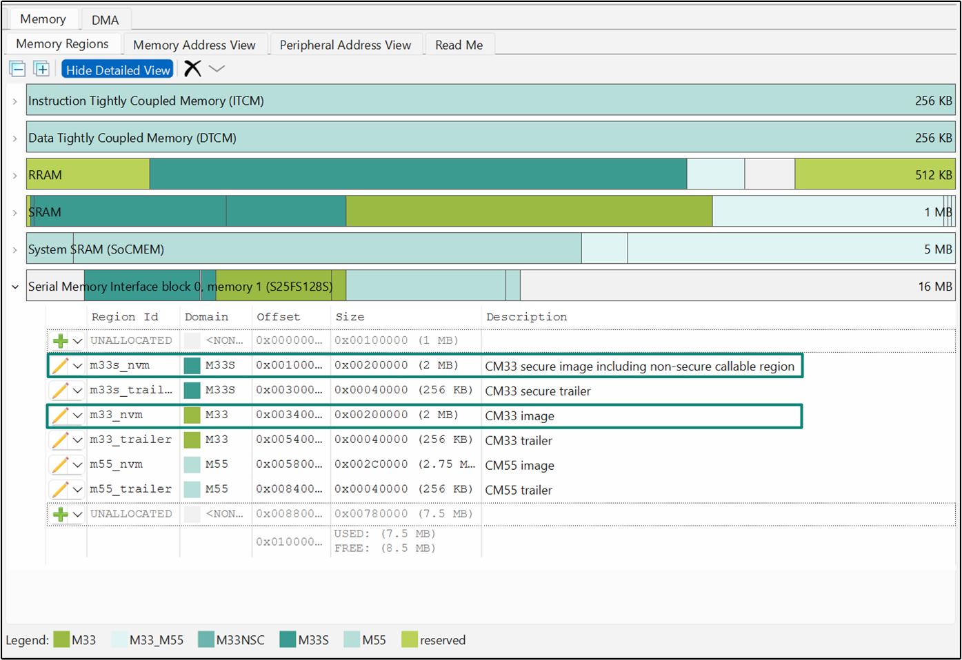
Click on the 'Pencil' icon located next to the
m33_s_nvm
memory region and select 'Edit Region' from the drop down menu to open the memory region editor window as shown in
Figure 11
. Alternatively, you may also select the memory region and press
F2
key on the keyboard to open the memory region editor window
Update the size of the
m33_s_nvm
region to
0x180000
(which corresponds to
1.5 MB
) as shown in
Figure 11
. Click on 'OK' to update the memory region
Figure 11.
Edit the memory region
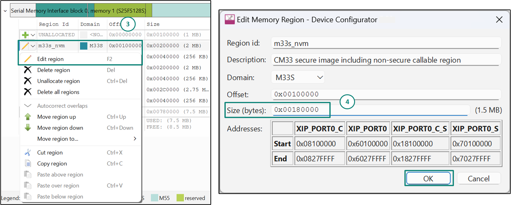
The memory region
m33s_trailer
require changes to its offsets, while its size shall remain the same. Follow the same procedure as in Step 3 to update the offsets as follows:
m33s_trailer
: Offset
0x280000
, Size
0x40000
(256 KB)
For the m33_nvm memory region, which corresponds to the cm33 non-secure image, both the offset and size need to be updated. Follow the same procedure as in Step 3 to modify the region as follows:
m33_nvm
: Offset
0x2C0000
, size
0x280000
(2 MB)
Once all updates are complete, verify that the final memory map matches the configuration shown in
Figure 12
. Save the design file to generate the linker files. The generated linker files for the custom memory layout will be present at
bsps/TARGET_<BSP>/config/GeneratedSource/
Figure 12.
Custom memory layout for external flash
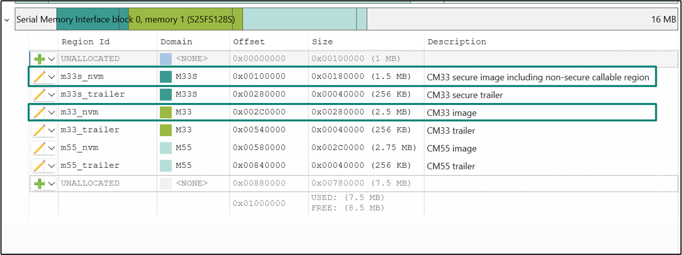
App start address
Placing and executing code from RRAM
By default, all three applications are located in the external flash connected on SMIF0, with RRAM serving as the sole internal NVM memory available for the
PSOC™ Edge
device. This section will focus on the process of placing and executing all three applications in RRAM. To achieve this, any basic code example for the
PSOC™ Edge
can be utilized, preferably
PSOC™ Edge
MCU: Basic Secure Application or
PSOC™ Edge
MCU: Hello world. The scope of customization is shown below.
Figure 13.
RRAM custom memory map
Note:
As the RRAM memory is very limited, the above use case is a demonstration rather than an actual production use case.
To achieve the target memory map as described, do the following:
Modify the memory layout in ModusToolbox™ Device Configurator to relocate the memory regions listed under (SMIF0) to RRAM
Update the combine-sign JSON file 'boot_with_extended_boot.json" for the following
Update the
metadata_proj_cm33_s
section with the RRAM hex address and slot-size of the CM33 secure project and update the fill value as
0x00
Update the
metadata_proj_cm33_ns
with the RRAM hex address of the CM33 non-secure project
Add a section
relocate_proj_cm55
to
shift
the CM55 hex from the Code AHB (C-AHB) address to the System AHB (S-AHB) address
Update the CM33 NS and CM55 project start location
Memory configuration in device configurator
To achieve the above use case, you need to make the following changes in the ModusToolbox™ Device Configurator:
Launch the ModusToolbox™ Device Configurator and navigate to the 'Memory' tab. Under the device's MPN (Manufacturer Part Number), review the default memory layout configuration, which displays the various memory regions supported by the device
Notice in
Figure 14
that the external flash memory listed under
Serial Memory Interface Block 0
(SMIF0) allocates the memory regions for CM33 secure project (m33s_nvm), CM33 non-secure project (m33_nvm) and CM55 project (m55_nvm) along with other accompanying memory regions. We shall move all of these regions to the RRAM section by deleting the memory regions in SMIF0 and creating the new regions with the same region name in
RRAM
section. Keeping the same memory region names will help us to use the default linker scripts of the BSP.
Figure 14.
Default memory layout for external flash
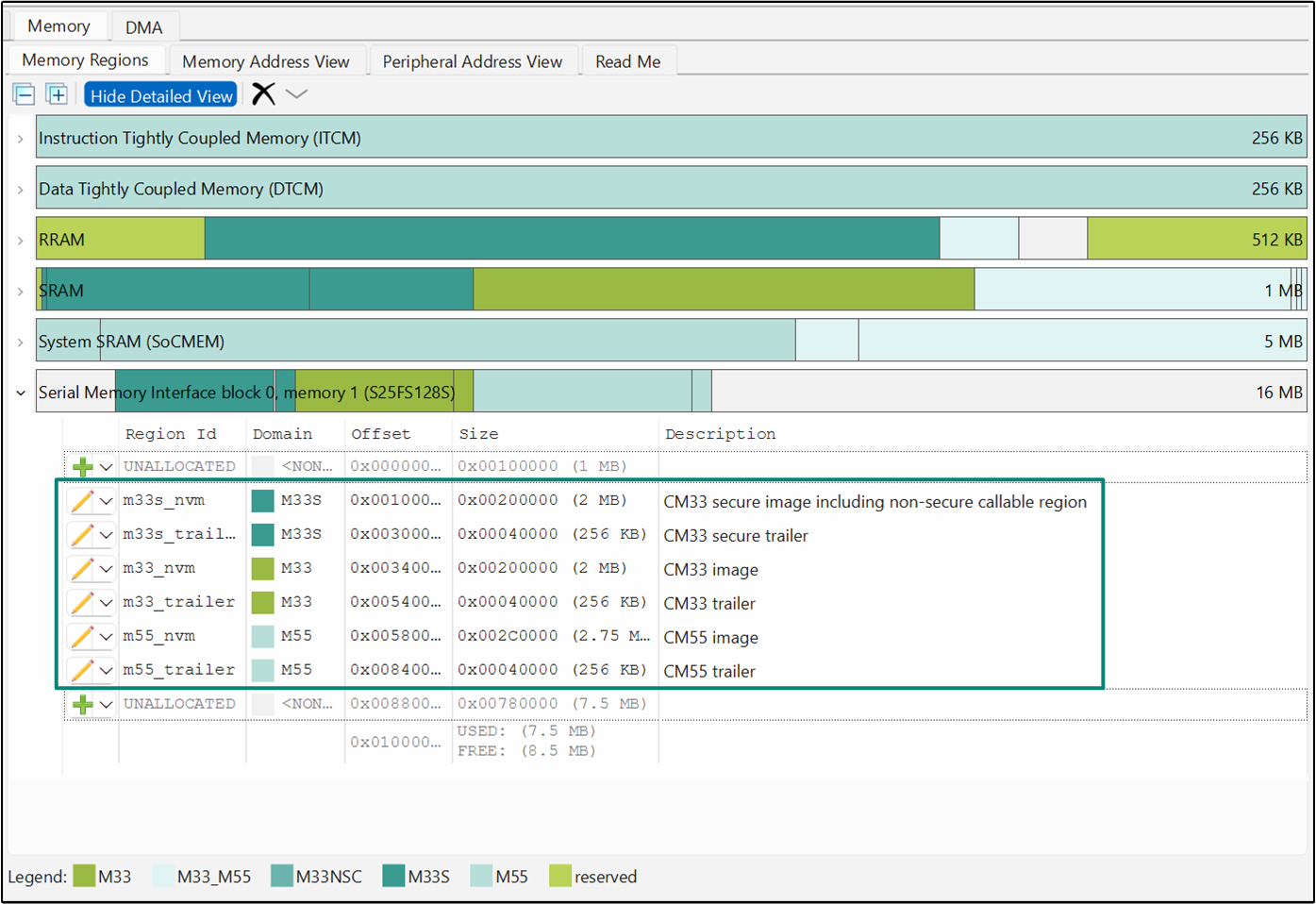
Click on the 'Pencil' icon located next to the
m33_s_nvm
memory region and select 'Delete all regions' from the drop down menu as shown in
Figure 15
. Alternatively, you may right-click on any memory region under SMIF0 and select 'Delete all regions' from the drop-down menu
Figure 15.
Delete all memory regions in external flash
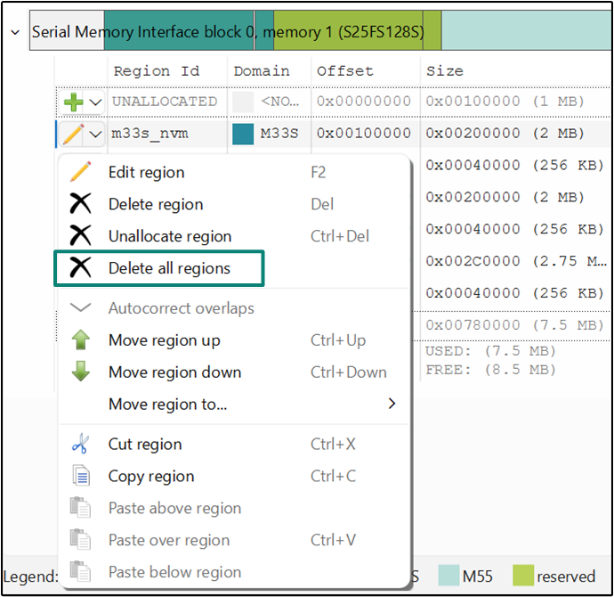
Under
RRAM
section, there is a predefined memory region
user_programmable
in the CM33 secure domain which is already located at default RRAM boot address for the CM33 secure app (
0x32011000
). We shall modify the name of this memory region as
m33s_nvm
to place the CM33 secure project and update the size of the memory region as 92 KB (
0x00017000
) as shown in
Figure 16
Figure 16.
Update the RRAM memory layout
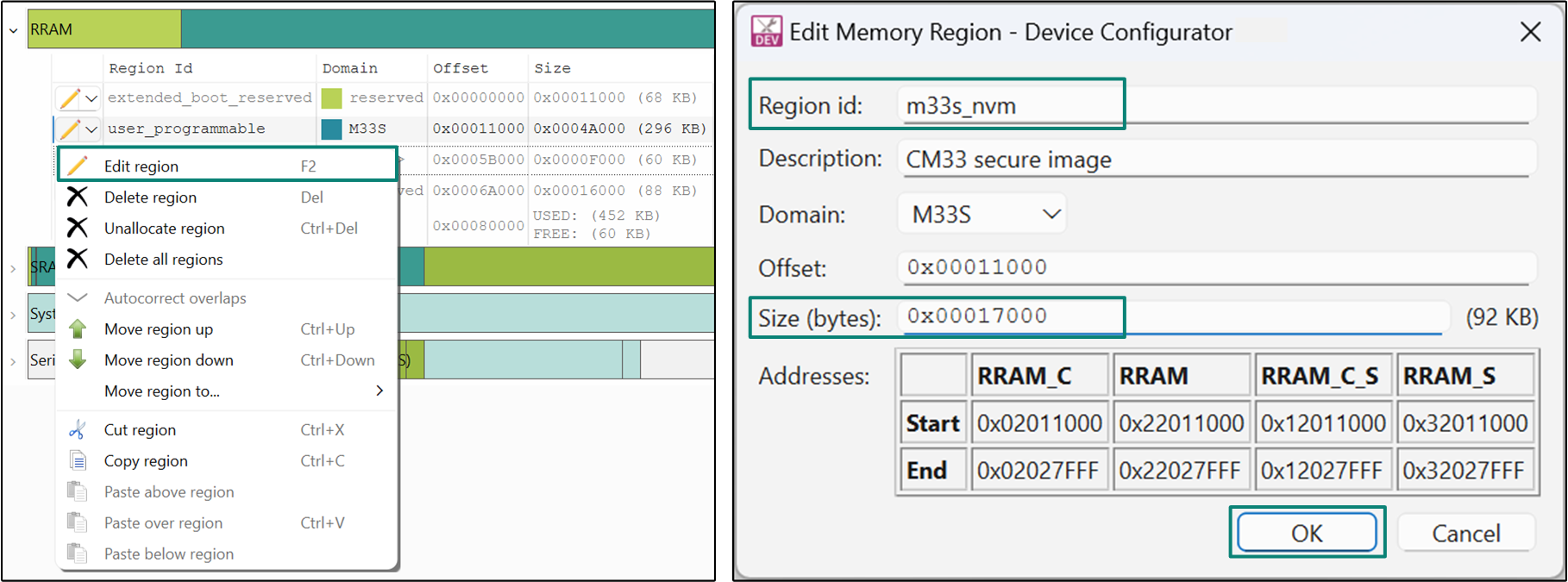
For the CM33 non-secure and CM55 projects, we shall create the corresponding memory regions with offsets and region sizes in the RRAM section as shown in
Figure 17
Figure 17.
Final RRAM memory layout
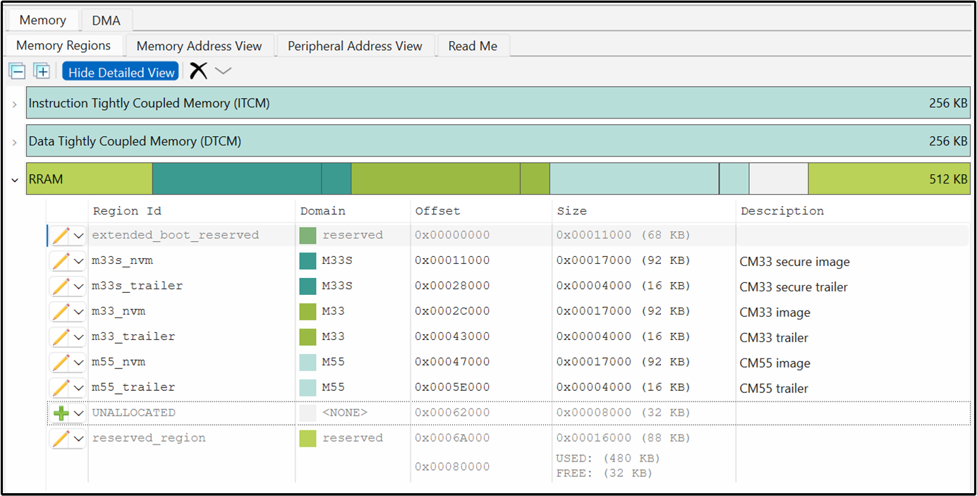
Verify the final memory map and save the design file to generate the linker files. The generated linker files for the custom memory layout will be present at
bsps/TARGET_<BSP>/config/GeneratedSource/
Update the combine-sign JSON file
The ModusToolbox™ Edge Protect Tools (packaged within the ModusToolbox™ Edge Protect Security Suite) uses the combine-sign JSON
boot_with_extended_boot.json
file present in the
<application-directory>/config
folder to sign, shift or manipulate the binary and Intel Hex (also known as
Intel hexadecimal object file format
) as needed by the application before combining them into a single final output
app_combined.hex
which is used for programming the MCU.
The default JSON file is configured to use the addresses of the external flash. We shall modify the file to use RRAM addresses. Following are the changes in the
boot_with_extended_boot.json
file.
Update the
'sign'
command under
metadata_proj_cm33_s
command group to use
0x00
as the fill value for RRAM. Update the slot-size to 108 KB (
0x1B000
) in the command
'inputs'
. The JSON snippet (with the update highlighted with underline formatting) is attached below.
{
    "name": "metadata_proj_cm33_s",
    "enabled" : true,
    "commands" :
    [
        {
            "command" : "sign",
            "inputs" :
            [
                {
                    "file" : "../build/project_hex/proj_cm33_s.hex",
                    "header-size": "0x400",
                    "fill-value" : "0x00",
                    "slot-size" : "0x1B000",
                    "hex-address" : "{{CYMEM_CM33_0_S_m33s_nvm_S_START}}"
                }
            ],
            .
            .
            .
        }
    ]
},
Create a new command group
relocate_proj_cm55
to
relocate
the CM55 hex from the Code AHB (C-AHB) address to the System AHB (S-AHB) address. This is done because the
C-AHB bus
supports only instruction fetches, preventing write operations to ensure security and efficiency in execute-only regions, such as Flash memory. In contrast, the
S-AHB bus
supports both read and write transactions, enabling versatile data communication between the CPU, SRAM, and peripherals for general-purpose operations. The relocation for CM33 non-secure image is already handled by the
relocate_proj_cm33_ns
command group in the same file. The JSON snippet for relocation of CM55 image is attached below
{
    "name": "relocate_proj_cm55",
    "description": "relocate the hex to a programmable (S-BUS) address",
    "enabled" : true,
    "commands" :
    [
        {
            "command" : "hex-relocate",
            "inputs" :
            [
                {
                    "file" : "../build/project_hex/proj_cm55.hex",
                    "regions" : "{{RelocationTable}}"
                }
            ],
            "outputs":
            [
                {
                    "file" : "../build/project_hex/proj_cm55_shifted.hex"
                }
            ],
            "extra_config":
            [
                {
                    "project": "proj_cm55",
                    "debug_config_name" : "proj_cm55",
                    "default":false,
                    "build_dependency" : "project"
                }
            ]
        }
    ]
},
Update the merge command group to use the new shifted hex file for the CM55 project,
proj_cm55_shifted.hex
. The JSON snippet (with the update highlighted with underline formatting) is attached below
{
    "name": "merge",
    "enabled": true,
    "commands" :
    [
        {
            "command" : "merge",
            "inputs" :
            [
                {
                    "file" : "../build/project_hex/proj_cm33_s_signed.hex"
                },
                {
                    "file" : "../build/project_hex/proj_cm33_ns_shifted.hex"
                },
                {
                    "file" : "../build/project_hex/proj_cm55_shifted.hex"
                }
            ],
            "outputs" :
            [
                {
                    "file" : "../build/app_combined.hex",
                    "format" : "ihex",
                    "overlap" : "ignore"
                }
            ]
        }
    ]
}
Save the
boot_with_extended_boot.json
file
App start address
By default, all code examples including the Hello World application, are configured to boot from the external QSPI flash connected through SMIF0. For all the three projects, booting from external flash, the S-AHB address is used. In order to launch the CM55 applications from RRAM, we must use the C-AHB address.
In the
main.c
file of the CM33 non-secure project, update the macro used for the application boot address of CM55 project as shown in the snippet below.
/* App boot address for CM55 project */
#define CM55_APP_BOOT_ADDR (CYMEM_CM33_0_m55_nvm_C_START + CYBSP_MCUBOOT_HEADER_SIZE)
Hardware (Boot switch) modification
By default, all code examples execute out of the external flash and extended boot launch CM33S from the external flash. To launch CM33 S from RRAM, ensure that BOOT_SWITCH (BOOT_SW) P6.0 is "Low(0)". See the Security user guide for more details.
Placing and executing code from SRAM
The default memory map places and executes all three projects (CM33 secure, CM33 non-secure and CM55) from the external flash connected on SMIF 0. Contrary to the default, this use case places the application in the external flash but loads and executes all three applications from SRAM at run-time. Code execution from SRAM provides better performance and lower power consumption.
For this use case, user shall refer to the
PSOC™ Edge
SRAM Loading
code example.
This code example provides instructions for loading all three projects into SRAM and requires the EdgeProtect Bootloader as an intermediate stage. The bootloader is programmed into the RRAM while the three projects are programmed into the external flash. On each system reset, the bootloader runs from RRAM, initializes the system, and copies the three application images into their assigned SRAM regions. After loading, the bootloader passes control to the CM33 secure project, and the application executes from SRAM.
See the README.md file of this code example for operation details.
Modifying the default stack size
Customizing the stack size is a critical consideration for ensuring reliable application performance, particularly in memory-constrained environments. This is particularly useful when an application involves complex operations, such as deep function call chains, recursive algorithms, or interrupt-heavy routines, which demand more stack space than the default allocation. Conversely, in simpler applications, reducing the stack size can free up valuable memory for other uses, optimizing overall resource utilization.
In the default linker scripts provided with the BSP, the stack size is defined as 4 KB (
0x1000
).
In order to modify the stack size of the project, the user needs to pass a linker flag in the project makefile.
LDFLAGS+= -Wl,--defsym=APP_MSP_STACK_SIZE=<CUSTOM_VALUE_IN_HEX>
Before modifying the stack size, developers should profile their application’s runtime behavior under expected operating conditions to estimate the stack space required for worst-case scenarios. Additionally, when increasing the stack size, developers must ensure that the total memory usage remains within the available SRAM bounds of the microcontroller.
Conclusion
This application note provides a comprehensive overview of the
PSOC™ Edge
architecture, including its power domains, internal and external memory configurations, bus architecture, memory access, default memory configuration, linker script usage, security configurations, power, and performance impact for memory accesses, as well as memory configuration cases. By understanding the intricacies of memory types, memory mapping, and optimization techniques, developers can effectively leverage the
PSOC™ Edge
's memory capabilities to enhance both power efficiency and overall system performance. Additionally, the note outlines various use cases for customizing memory maps and executing applications from different memory regions, offering valuable insights for optimizing memory usage in
PSOC™ Edge
-based designs.
References
Webpage
Infineon Technologies AG:
PSOC™ Edge Arm® Cortex® Multicore
;
Available online
Application notes
Infineon Technologies AG:
AN237976:
PSOC™ Edge
E8 MCU low power modes and power reduction techniques
;
Available online
Infineon Technologies AG:
AN235935: Getting started with
PSOC™ Edge
E8 on ModusToolbox™ software
;
Available online
Infineon Technologies AG:
AN237849: Getting started with
PSOC™ Edge
security
;
Available online
Code examples
Infineon Technologies AG:
CE238541:
PSOC™ Edge
MCU: Hello world
;
Available online
Infineon Technologies AG:
CE238537:
PSOC™ Edge
MCU: Basic Secure Application
;
Available online
Infineon Technologies AG:
CE238579:
PSOC™ Edge
MCU: PSRAM Read and Write in Execute in Place (XIP) mode
;
Available online
Infineon Technologies AG:
CE238563:
PSOC™ Edge
MCU: Serial Flash Read and Write
;
Available online
Infineon Technologies AG:
CE240902:
PSOC™ Edge
MCU: SRAM Loading
;
Available online
Revision history
Document revision | Date | Description of changes |
|---|---|---|
*B | 2025-09-04 | Release to web |
Trademarks
PSOC™, formerly known as PSoC™, is a trademark of Infineon Technologies. Any references to PSoC™ in this document or others shall be deemed to refer to PSOC™.