AN239191 Getting started with graphics on PSOC™ Edge MCU
About this document
Scope and purpose
This application note describes how to get started with the graphics subsystem on
PSOC™ Edge
MCU. It talks about basic graphics concepts and introduces the hardware and software components of the graphics subsystem. Furthermore, it also provides a hands-on walk-through on how to create a graphics application from scratch on the
PSOC™ Edge
MCU using ModusToolbox™.
Intended audience
This application note is tailored for hardware and software developers, engineers, and system architects who are involved in the design and development of graphical applications using the
PSOC™ Edge
MCU. It is also suitable for anyone seeking a brief understanding of graphics subsystem on
PSOC™ Edge
MCU.
Introduction
Note:
The initial sections (sections 1 through 4) introduce the graphics capability of
PSOC™ Edge
MCU including an introduction to basic graphics concepts and an overview of the Graphics Subsystem hardware and software resources. To quickly get started by creating a sample application, jump directly to section 5
Graphics application design on PSOC Edge MCU
.
PSOC™ Edge
MCU brings with itself a high performance and low-power graphics subsystem to enable human-machine interface (HMI) based application development.
This application note introduces you to the graphics capabilities of the
PSOC™ Edge
MCU, providing an overview of the graphics subsystem, and gets you started with a simple graphics application using VGLite graphics API wherein you learn to develop and render 2.5D vector and raster graphics using the
PSOC™ Edge
MCU. This application note helps you to develop your graphics application from scratch with an empty starter application template. To illustrate a fully functional graphics application, code examples for ModusToolbox™ are also provided.
This application note covers the introduction to graphics subsystem on
PSOC™ Edge
MCU. See
AN235935 Getting Started with
PSOC™ Edge
E8 MCU on ModusToolbox™
for an overview and getting started for application development on the
PSOC™ Edge
MCU.
The graphics subsystem has following features. The hardware resources are described in the
Graphics subsystem hardware resources
section and the software resources in the
Graphics subsystem software resources
section.
Supports display size up to 1024 × 768 pixels @ 60 Hz (64 MHz) with 24-bit color resolution with all modes of the RGB color palette like RGB888, ARGB8888, RGR565 and so on
DPI up to 64 MHz pixel clock, for example 1024 × 768 @ 60 Hz (Via MIPI-DSI)
DBI up to 16 bits @ 50 MHz (GPIO) or 37.5 MHz (MIPI-DSI)
Independent GPU and display controller
MIPI display compatibility
MIPI-DSI, D-PHY
MIPI Display Bus Interface (DBI) Type C, Type B
Related code examples
This application note introduces and demonstrates the code example "
PSOC™ Edge
MCU: Graphics using VGLite API
", where the VGLite Graphics APIs are used to carry out hardware-accelerated 2D vector drawing operations and render the generated image on a TFT LCD. The code example is also available on
GitHub
. The LCD is connected via the Mobile Industry Processor Interface Display Serial Interface (MIPI DSI).
Additionally, the following code examples using the graphics subsystem on the
PSOC™ Edge
MCU. These applications can be evaluated by creating a project using ModusToolbox™ Project Creator. All the below code examples use the Waveshare 4.3-inch Raspberry Pi DSI LCD Display by default.
PSOC™ Edge
MCU: Graphics LVGL Demo
This code example showcases how to exhibit a 2D graphics demonstration on an LCD, by employing the Light and Versatile Graphics Library (LVGL) on a
PSOC™ Edge
MCU. It displays a music player application, which is listed as one of the standard demos on the LVGL page. The LCD is connected via the MIPI Display Serial Interface (DSI) and the code is designed to run in a FreeRTOS environment.
See the code example on
GitHub
PSOC™ Edge
MCU: Graphics using RLAD
This code example demonstrates how to utilize the Run-Length Adaptive Dithering (RLAD) decoder present in the graphics subsystem of
PSOC™ Edge
MCU to decompress and display RLAD encoded images in real-time. The decompressed image is displayed on a TFT LCD. The LCD is connected via the MIPI Display Serial Interface (DSI)
See the example on
GitHub
PSOC™ Edge
MCU: Graphics rendering using CPU vs GPU
This code example demonstrates the graphics displaying capabilities of
PSOC™ Edge
MCU by displaying an image on a TFT LCD using either of the following two methods:
GPU-disabled (No hardware acceleration): The target image's pixel data array (16-Bit RGB565) is directly used without using GPU
GPU-enabled (Hardware acceleration): The target image's vector data paths are used with Vivante's platform-independent VGLite Graphics APIs to carry out hardware-accelerated 2D vector drawing operations
The resulting image is displayed on a TFT LCD. The LCD is connected via the MIPI Display Serial Interface (DSI)
See the example on
GitHub
PSOC™ Edge
MCU: Graphics using single and double buffering
The code example showcases how to use the graphics subsystem of
PSOC™ Edge
MCU to render images on an LCD screen, utilizing either single or double buffering mode:
Single buffering: A single buffer is used for draw and display the image frames sequentially
Double buffering: This process involves using one buffer to create a frame while another buffer is simultaneously utilized to display the previously composed frame. In continuous mode (video burst), the buffers are swapped and used in a ping-pong fashion in the next iteration
The double buffering technique provides the advantage of improved throughput over the single buffering technique by removing the flicker effect which may occur in the latter mode due to frames being drawn more quickly than the rate at which they are being displayed. Since the frame drawing and displaying can take place in a parallel manner in double buffering, the flickering is reduced considerably.
The images are displayed on a TFT LCD. The LCD is connected via the MIPI Display Serial Interface (DSI)
See the example on
GitHub
PSOC™ Edge
MCU: Graphics DSI ULPM On Data Lane
This code example demonstrates entry and exit in MIPI Display Serial Interface Ultra Low Power Mode (DSI ULPM) on data lane only. In this mode, the DSI PHY state machine is entering a low-power state on data lane and allows to save some power when the LCD does not need to display. When the display is needed again, the DSI ULPM on data lane is exited and display should operate as before. This code example uses a TFT LCD connected via MIPI DSI interface
See the example on
GitHub
PSOC™ Edge
MCU: Smartwatch demo using LVGL
This code example highlights Infineon's comprehensive support for high-performance and low-power graphics applications on
PSOC™ Edge
MCU. It showcases a Graphical User Interface (GUI) implementation of a smartwatch, primarily using a 1.43-inch round AMOLED display in 466*466 resolution. This code example also implements the emulation of the round smartwatch GUI in the same resolution on a 4.3-inch Raspberry-Pi TFT display. This application demonstrates the ability to leverage the Graphics Processing Unit (GPU) for high-performance GUI rendering, as well as a CPU-rendered low-power always-on screen. The GUI is powered by LVGL.
See the example on
Github
Supported displays
lists the displays supported for
PSOC™ Edge
MCU, their feature description and their associated display and touch drivers.
Display name | Feature description | Display driver IC and Library | Touch driver IC and Library |
|---|---|---|---|
Waveshare 4.3-inch DSI LCD | 4.3 inch 800x480 DSI Capacitive Touch Display panel | ICN6211 | FT5406 |
Winstar WF101JTYAHMNB0 | 10.1 inch MIPI IPS TFT Display 1024 × 600 with Projective Capacitive (PCAP) touchscreen | EK79007AD3 | ILI2511 |
Dastek 1.43-inch circular display | 466 × 466 AMOLED Capacitive Touch Panel (CTP) MIPI-DSI Display | CO5300 | FT6146 |
Microtek 1.43-inch circular display | 466 × 466 AMOLED Capacitive Touch Panel (CTP) MIPI-DSI Display | CO5300 | FT3268 |
Waveshare 7-inch DSI LCD ( C ) | 7 inch 1024 × 600, R-Pi compatible, 15-pin connector | ICN6211 | GT911 |
Basic graphics concepts
This section covers some frequently used terminologies and concepts in the context of embedded graphics and display technology. This is not an exhaustive list but covers the essential concepts to help you get started with development of graphics applications on
PSOC™ Edge
MCU.
Pixels
A pixel (short for picture element) is the smallest unit of a digital image or display. It is a very small, isolated dot that stands for one color and plays the most basic part in digital images. Pixels when combined help to create the mosaic of colors and shapes contributing towards visual content being displayed on screens.
Depending on the color format of the image, a pixel may take up from just 1 bit of memory to 32 bits or more. The memory space occupied by each bit is called bit depth and usually measured in bits per pixel
RGB color palette
In computer graphics, a palette is the set of available colors from which an image can be made. The most commonly used multi-color palette is the RGB palette which is a color model formed using red, green and blue colors. The basic idea behind representing colors with these three primary color components is that the superimposition of these three colors in different percentages can be used to reproduce a wide range of visible colors.
The RGB palette comes with different pixel color formats of varying bit depths. Usually, the color formats have same number of levels for red, green and blue components but its not necessary as we see the case with RGB565. Some common examples are captured in the following table.
Table 2.
RGB palette
RGB color format
Description
RGB888
24 bits, 8 bits per component. (true color)
ARGB8888
32 bits, 8 bits per component (8 bits alpha, 24 bit RGB color)
RGB666
18 bits, 6 bits per component.
RGB565
16 bits, 5 bits red, 6 bits green, 5 bits blue (High color)
ARGB2222
8 bits, 2 bits per component (2 bits alpha, 6 bit RGB color)
GRAY4
4 bits grayscale
GRAY2
2 bits grayscale
BW
1 bit grayscale (Black and White)
The RGB color model is one of the most common ways to encode color in computing, and several different digital representations are in use. The main characteristic of all of them is the quantization of the possible values per component (technically a sample ) by using only integer numbers within some range, usually from 0 to some power of two minus one (2^n − 1) to fit them into some bit groupings
Bit depth
Bit depth describes the level of detail for the color information stored in an image. The higher the bit depth an image has, the more colors it can store. Bit depth is sometimes also known as bits per pixel or color depth and is defined as the number of bits used to define each pixel. For example, an image with color format of RGB888 has a bit depth of 24 bits.
Images with higher bit depth can store more colors and result in a smoother image. The lower the bit depth is for an image, the more likely you are to see sharp delineations between color changes in the images. However, images with higher bit depth are heavy on CPU and GPU utilization while also taking up more space in the memory.
The selection of an appropriate bit depth for images in an embedded system is generally based off a tradeoff between image quality and MCU memory and CPU resource availability
Resolution
The resolution of a display is the number of distinct pixels in each direction (horizontal and vertical) that can be displayed. It is usually expressed in (Width × Height) format where "Width" and "Height" are the number of pixels in Horizontal and vertical direction respectively
Display resolution is also sometimes expressed in pixels per inch (PPI) which refers to the number of pixels that can be displayed over one inch of the screen or display. A high PPI means there are more pixels in every inch, which results in a higher resolution and a crisper image. If the image has a low PPI, it results in a blurry image that's difficult to see and interpret
Alpha channel
The alpha channel is a component of the pixel which represents the degree of opacity (also defined as transparency) of a digital image. This transparency information is stored in addition to the actual image data. Certain image color formats may or may not include the transparency channel, and also the channel width (alpha bit depth) can vary across different formats
For example, an image with the color format of ARGB8888 has a total bit depth of 32 bits per pixel (bpp) including an 8-bit alpha channel with the 24-bit RGB color palette
Image compression
In embedded systems with memory constraints, images are usually stored with some degree of size reduction. This is done using image compression algorithms and it results in smaller memory footprint while in storage. However, the compressed image must be decoded and decompressed before displaying on the screen.
Lossy
: Lossy image compression compresses the data in the image to a point that some information is lost (quality is reduced), but storage space is saved at the expense of quality. JPEG is a well known standard for compressing images
Lossless
: Lossless image compression stores the image in such a way that it occupies less storage space than an uncompressed image, but no information is lost. The original image can be reproduced exactly as it was before compression
An example of lossless image compression is Run-length Encoding (RLE). In this method, sequences that display redundant data are stored as a single data value. This value represents the repeated block, and shows how many times it appears in the image. During decompression, the image can be reconstructed exactly from this information. See
Related code examples
for a reference application featuring the Run-Length Adaptive Dithering (RLAD) decoder present in the graphics subsystem of
PSOC™ Edge
MCU
Frame rate and refresh rate
Frame rate, most commonly expressed in frames per second or FPS, is typically the frequency (rate) at which consecutive images (frames) are being generated by the computer or graphics engine system within itself or in some memory buffer. It determines the smoothness and fluidity of motion on the screen. The higher the FPS, the smoother the movement appears to be. The reason for this is that a higher number of frames per second creates more realistic and seamless visuals.
In an embedded system, the frame rate is a function of multiple factors like the speed of the memory, processing capability of the CPU and the GPU and the composition of the image or video being displayed.
The refresh rate is defined as the number of times per second the display is able to draw a new image from the frame buffer. Refresh rate is a property of the display only and is usually measured in Hertz
Frame buffer and multi-buffering
The frame buffer is a memory (usually in RAM), which holds the data to be shown on the display screen and acts as the data source for the display controller. The required size of the frame buffer depends on the resolution and color depth. The minimum requirement is that it should hold the data required to display one full frame and must support the scan rate (preferred refresh rate as per the data sheet of the display) of the display controller.
The amount of colors and the number of pixels in the frame buffer determines the memory consumed by the frame buffer. The amount of memory used by a frame buffer can be calculated as follows:
Size of Frame Buffer (in bytes) = (width * height * color depth in bits / 8)
When having more than one frame buffer the amount of memory consumed will be correspondingly larger. For example when having a double buffering scheme, using two frame buffers, will consume twice the amount of memory.
Multi-buffering is a scheme used to enhance display performance by having two or more frames ready just in time for the display frame update. Double buffering is a common example, where we keep two separate frame buffers where we have one frame buffer to draw the image, while the other buffer which contains an already complete frame, feeds to the display. This is typically used when separate hardware works together in a graphics application; for example the GPU composes the image in one buffer while the content of the other buffer is sent to the display in the background by the display controller.
See
Related code examples
for a reference application featuring the single and double buffering mechanism using the Graphics subsystem of
PSOC™ Edge
MCU
Graphics subsystem hardware resources
The graphics subsystem on
PSOC™ Edge
MCU consists of following blocks
Graphics Processing Unit (GPU)
Display Controller (DC)
MIPI DSI Host Controller
The functional relationship among the blocks of the graphics subsystem is shown in
Figure 1
. For detailed discussion on these components, see Graphics Subsystem section in the
PSOC™ Edge
Architecture Reference Manual.
Figure 1.
PSOC™ Edge
Graphics Subsystem
GPU block
The GPU is a standalone hardware block controlled by software commands issued through a command FIFO (first-in, first-out) buffer. It accelerates 2D affine operations on graphical data, including scaling, rotation, and translation, and it supports pixel blending for composition.
It supports multiple pixel formats and image interpolation modes, with bit depths ranging from 1 to 32 bits per pixel. For the complete list of supported formats, see the “Format Support” section in the Graphics Subsystem chapter of the
PSOC™ Edge
Architecture Reference Manual
.
The Graphics subsystem, including the GPU, is configured and initialized using the Infineon Peripheral Driver Library (PDL). After initialization, the GPU is controlled via the VGLite Graphics API (Application Programming Interface), which provides the command and control interface for rendering.
The VGLite Graphics API is designed for menu-driven user interfaces and optimized for resource-constrained systems. It is intended to deliver high rendering performance while minimizing memory footprint, provides fine-grained control over memory usage, and is well suited to deployments where only a single rendering class is required.
Display controller
The Display Controller (DC) transfers rendered frames from the frame buffer to the display pipeline. In addition to driving the output interface, it provides hardware cursor support and applies pixel processing stages such as format conversion, dithering, and gamma correction. The controller supports Display Pixel Interface (DPI) and Display Bus Interface (DBI). On
PSOC™ Edge
devices, only DBI is exposed on package pins; the DPI connection is used internally by the MIPI DSI host controller.
DC output is available either on general-purpose I/O as DBI (including SPI-based DBI variants) or through the MIPI DSI PHY. The DC and the MIPI DSI host/controller are programmed via the host register interface, while pixel data is fetched from system memory over a dedicated bus independent of the host interface. The GPU and the DC/MIPI DSI blocks operate independently; each can be used without the other.
The GPU autonomously reads pixel data from memory, performs the configured processing, and writes the results back to memory. The DC then sources pixels from memory and transmits them to the panel. There are two possible data paths for the pixel data to be sent to the display as discussed in following points, however only one type of display at a time is supported.
From the memory via the DC controller to the DBI interface to the display
From the memory via the DC controller and the MIPI DSI interface to the display
MIPI DSI controller
The MIPI DSI host controller gets image information from the display controller in a DPI or DBI format depending on the sink display type. The controller can drive displays with built-in memory (Command mode) and without built-in memory (Video mode). MIPI DPI is used in video mode while MIPI DBI is used in command mode. The pixel flow diagram combining the three hardware components of the graphics subsystem is shown in
Figure 2
.
Figure 2.
Pixel data flow
The GPU first reads the commands from the memory and outputs the resultant frame to a display buffer in the memory. The display controller now reads the frame buffer(s) to generate the final graphic. The display controller can either send the image directly to digital outputs for DBI Type A/B or SPI (Type C) displays or it can send the image to the DSI Host controller for DSI displays.
Graphics subsystem software resources
To support the development of graphical applications on the hardware, a host of software resources are available for the
PSOC™ Edge
MCU.
Figure 3
shows the overall software architecture of
PSOC™ Edge
graphics subsystem.
Figure 3.
Software architecture
The application code is at the top layer of the software architecture. This is where the firmware design of the application is formalized. After the application layer, there is panel driver library which is specific to a particular display. It initializes the display panel with parameters like brightness control, sleep modes, display formats. Similarly, there is a touch driver library which is used to initialize the touch interface if available on the display.
As part of the graphics framework, the Light and Versatile Graphics Library (LVGL) which is a free and open-source graphics library which provides all the necessary software components to create an embedded GUI application with easy-to-use graphical elements, while also maintaining a low memory footprint is available. See Related code examples for a reference application designed using the LVGL library on
PSOC™ Edge
MCU.
VGLite provides APIs for vector graphics functionality to carry out hardware-accelerated 2D vector drawing operations and renders the generated image. The display controller driver drives standard IO pins with DBI-A, DBI-B, and DBI-C interfaces. Additionally, the display controller driver is the video source for MIPI DSI block and related display interfaces. The MIPI DSI driver allows to configure the MIPI DSI Host Controller input by either Display Pixel Interface (DPI) or Display Bus Interface (DBI) and drive MIPI DPHY interface.
Next, the device configurator generates code using the Infineon device support library for
PSOC™ Edge
MCU. There is a dedicated personality in the configurator which allows the user to easily configure graphics settings for the specific application. See section
Setting up Device Configurator to use the graphics subsystem
for more details. You can also directly use the device support library APIs bypassing the device configurator to initialize and use the graphics subsystem.
Graphics application design on PSOC™ Edge MCU
This section covers the steps to create, build, and run the application.
Create a new application
Configure design resources
Write the application code
Build, program, and test your design
These instructions require a particular code example (
PSOC™ Edge
MCU: Graphics using VGLite API in this case). However, the extent to which you use the code example (CE) depends on the method you follow through these instructions.
Table 3
lists the two defined methods on these instructions depending on what you want to learn.
Method | Best for |
|---|---|
“Using CE directly” (evaluate existing code example (CE) directly) | If you are new to the tool or device, and want to see how it all works quickly |
“Working from scratch” (use existing code example (CE) as reference only) | If you want the hands-on experience to learn to develop PSOC™ Edge -based graphics applications in ModusToolbox™ |
Respective sections of each option provide the instructions.
If you start from scratch and follow all instructions in this application note, you must use the code example as a reference while following the instructions. Working from scratch helps you learn the design process and takes more time. Alternatively, you can evaluate the existing code example directly to get acquainted with the
PSOC™ Edge
development flow in a short time.
See the sections from the
Prerequisites
and go through the
Firmware description
in both the cases.
Prerequisites
Make sure that you have the appropriate graphics capable development kit for the
PSOC™ Edge
E8 MCU product line. See the device datasheet for details. Throughout this application note, we will use the
PSOC™ Edge
E84 Evaluation Kit as the reference platform for demonstartion
Refer to the
AN235935 - Getting started with
PSOC™ Edge
E8 MCU on ModusToolbox™ software
application note for hardware and software prerequisites. Additionally,
Install any Terminal Emulator on your PC. Teraterm is used/shown in this design
This application note uses a project which drives a Waveshare 4.3-inch DSI LCD. The LCD houses a Chipone ICN6211 display controller and uses the MIPI DSI interface. If using other displays, the user must add the display and touch driver libraries for the display using ModusToolbox™ Library Manager. See
Add libraries and middleware
Supported Displays and their electrical connections with the
PSOC™ Edge
E84 Evaluation Kit
Waveshare 4.3-inch Raspberry-Pi DSI LCD 800*480 pixel display
:
The kit supports this display by default. No hardware rework or board modifications are required. to use this display.
Connect the 15‑pin FPC cable between the display’s FPC connector and the
PSOC™ Edge
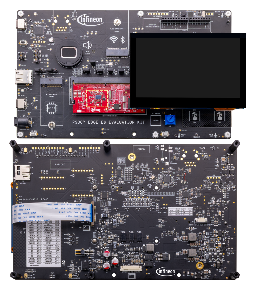
E84 board’s R-Pi compatible MIPI DSI connector (J39), as shown in the
Figure 4
. Align pin 1 on both connectors, open the latch before insertion, fully seat the cable, and then secure the latch to ensure a reliable connection.
Figure 4.
Waveshare 4.3-inch Raspberry Pi DSI LCD connection
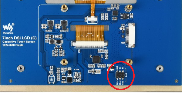
Waveshare 7-inch Raspberry-Pi DSI LCD C 1024*600 pixel display
: The figure below highlights the header named 'FAN' on the display supporting I2C interface.
Figure 5.
Waveshare 7-inch Raspberry Pi DSI LCD (C) display's I2C connection (FAN connector)
Interface the display with the
PSOC™ Edge
E84 Evaluation Kit using the connections outlined in the table below.
Table 4.
Display and evaluation kit connections
Display's Connector
PSOC™ Edge
E84 Evaluation Kit's connector
DSI connector
J39
GND (FAN)
GND (J41)
5V (FAN)
5V (J41)
SCL (FAN)
I2C_SCL (J41)
SDA (FAN)
I2C_SDA (J41)
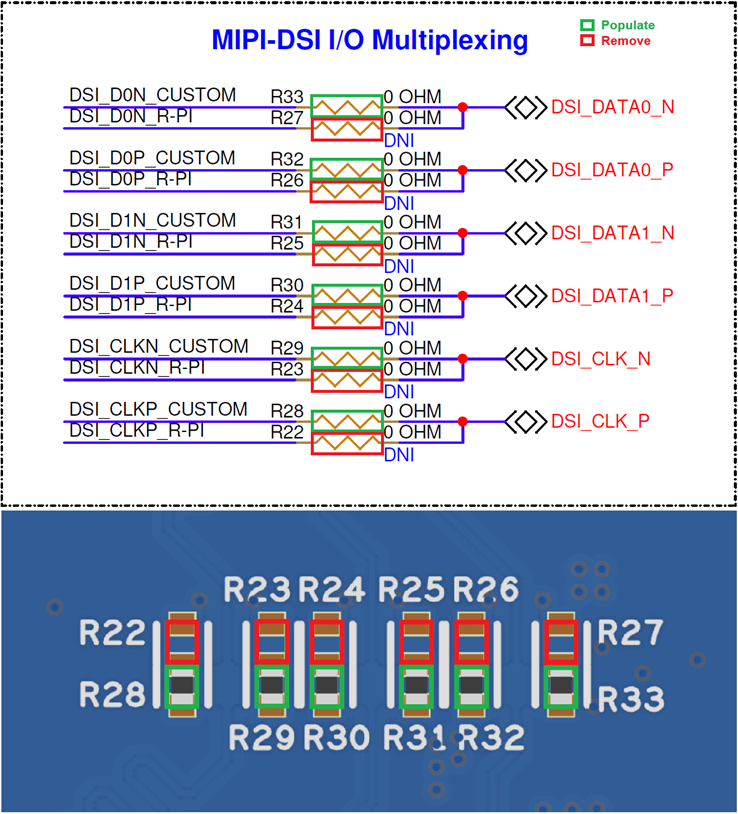
10.1 inch 1024*600 pixel TFT LCD (WF101JTYAHMNB0) display:
Using this setup requires rework on the
PSOC™ Edge
E84 Evaluation Kit, and the rework instructions are as follows:
Remove:
R22, R23, R24, R25, R26, R27
Populate:
R28, R29, R30, R31, R32, R33
Figure 6.
Rework on
PSOC™ Edge
E84 base board
Interface the display with the
PSOC™ Edge
E84 Evaluation Kit using the connections outlined in the table below.
Table 5.
Display and evaluation kit connections
Display's Connector
PSOC™ Edge
E84 Evaluation Kit's connector
DSI connector
J38
Touch connector
J37
Note:
If you are using the 10.1-inch LCD, it may be required to additionally connect a second USB cable to the device port or the 12 V DC adapter to power up the display
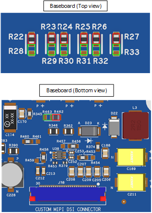
1.43-inch circular 466x466 AMOLED displays:
Using this setup requires rework on the
PSOC™ Edge
E84 Evaluation Kit, and the rework instructions are as follows:
Remove:
R22, R23, R24, R25, R26, R27, R462
Populate:
R28, R29, R30, R31, R32, R33, R463
Figure 7.
Rework on
PSOC™ Edge
E84 base board
Interface the display with the
PSOC™ Edge
E84 Evaluation Kit using the connections outlined in the table below.
Table 6.
Display and evaluation kit connections
Display's Connector
PSOC™ Edge
E84 Evaluation Kit's connector
DSI connector
J38
Touch connector
J37
About the design
The design of this application is kept straightforward to help the user get started with code examples on
PSOC™ Edge
MCU devices. All
PSOC™ Edge
MCU applications have a dual-CPU three-project structure to develop code for the CM33 and CM55 cores. The CM33 core has two separate projects for the Secure Processing Environment (SPE) and Non-secure Processing Environment (NSPE). A project folder consists of various subfolders – each denoting a specific aspect of the project. See
Figure 15
for the application flowchart.
In this code example, at device reset, the secure boot process starts from the ROM boot with the secure enclave (SE) as the root of trust (RoT). From the secure enclave, the boot flow is passed on to the system CPU subsystem where the secure CM33 application starts. After all necessary secure configurations, the flow is passed on to the non-secure CM33 application. Resource initialization for this example is performed by this CM33 non-secure project. It configures the system clocks, pins, clock to peripheral connections, and other platform resources. It then enables the CM55 core using the
Cy_SysEnableCM55()
function and the CM33 core is subsequently put to DeepSleep mode.
In the CM55 application, the clocks and system resources are initialized by the BSP initialization function. The retarget-io middleware is configured to use the debug UART. The debug UART prints a message on the serial terminal. The onboard KitProg3 acts the USB-UART bridge to create the virtual COM port.
The CM55 application drives the LCD and renders the image using the
PSOC™ Edge
graphics subsystem. The GPU supports vector graphics (drawing circles, rectangles, quadratic curves) and font support. This code example implements operations like rotate/scale, color fill, and color conversion. After the GPU renders the frames, they are transferred to the MIPI DSI host controller via the DC and displayed on the LCD.
See
README.md
file of the application
PSOC™ Edge
MCU: Graphics using VGLite API
for more details.
Create a new application
This section provides you step-by-step instructions to create a new ModusToolbox™ application. Before performing the steps in this section, decide whether you want to create and run the code example as-is or you want to learn how to create an application from scratch. Depending on your need, choose from the following:
“
Using CE directly
” (evaluate existing code example (CE) directly)
Follow the sections:
Ignore the following section:
“
Working from scratch
” path (use existing code example (CE) as reference only)
Follow the sections:
Ignore the following section:
Select a new workspace
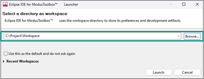
At launch, ModusToolbox™ presents a dialog box to choose a directory as the workspace directory. The workspace directory is used to store workspace preferences and development artifacts such as device configuration and application source code.
You can choose an existing empty directory by clicking the Browse button. Alternatively, you can type in a directory name to be used as the workspace directory along with the complete path, and ModusToolbox™ will create the directory for you.
Figure 8.
Select a directory as a workspace
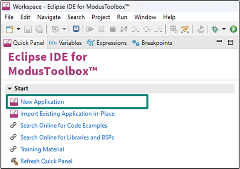
Create a new application
Click
New Application
(see
Figure 9
) in the Quick Panel. Alternatively, go to
File > New
and click ModusToolbox™ application.
Figure 9.
Create a ModusToolbox™ application
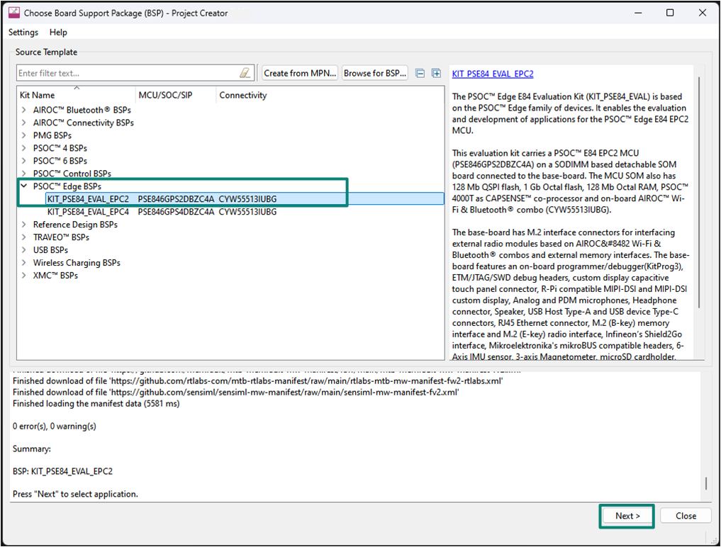
Select
PSOC™ Edge
E84 MCU-based target hardware
ModusToolbox™ shows the list of Infineon kits to start your application development. In this case, we will develop an application on the
PSOC™ Edge
E84 Evaluation board. Select
KIT_PSE84_EVAL_EPC2
and click Next, as shown in
Figure 10
.
Figure 10.
Choose target hardware
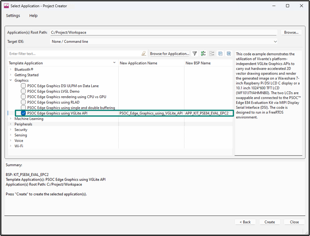
Create the graphics using VGLite API code example (applicable only for the “Using CE directly” flow)
Create an existing code example (Graphics using VGLite API code example) in the Eclipse IDE for ModusToolbox™. Do this for the “Using CE directly” flow.
shows the Select Application window of the Project Creator tool
Select the
PSOC™ Edge
MCU: Graphics using VGLite API
application under 'Graphics', and optionally, in the New application Name field, change the name of the application
Click Create and wait for the application to get downloaded and created in the workspace
Click Close to complete the application creation process
Figure 11.
Create Graphics using VGLite API code example
Select a starter application and create the application (applicable only for “Working from scratch” flow)
Use an existing empty application as the starting point for the “Working from Scratch” development flow. This is a minimal starter application template for
PSOC™ Edge
MCU devices. This example uses FreeRTOS to blink two LEDs with different frequencies respectively from the Arm® Cortex®-M33 CPU and the Arm® Cortex®-M55 CPU.
This code example has a three project structure (that is, CM33 secure, CM33 non-secure, and CM55 projects). All three projects are programmed to an external QSPI flash and executed in the XIP mode. Extended Boot launches the CM33 secure project from a fixed location in an external flash, which then configures the protection settings and launches the CM33 non-secure application. Additionally, the CM33 non-secure application enables the CM55 CPU and launches the CM55 application.
The application code of the
PSOC™ Edge
MCU: Graphics using VGLite code example uses only the CM55 CPU. Therefore, the application is written under the CM55 project (proj_cm55) and the CM33 CPU (in proj_cm33_ns) is subsequently put to DeepSleep.
To create an Empty_app, in the Select Application window (see
Figure 12
), select PSOC_Edge_Empty_Application
In the Name field, type in a name for the application if required and click Next; the application summary dialog appears
Click Create and wait for the application to get downloaded and created in the workspace. Click Close to complete the application creation process
Figure 12.
Create a starter application
You have successfully created a new ModusToolbox™ application for the
PSOC™ Edge
MCU.
Configure design resources
In this step, configure the design resources for your application and generate the configuration code. You will also add the required middleware libraries.
Method | Action |
|---|---|
“Using CE directly” (evaluate existing code example (CE) directly) | Read and understand all steps. The CE has the resource configurations done; therefore, you do not need to perform any of the steps in this section. |
“Working from scratch” (use existing code example (CE) as reference only) | Perform all steps. |
Add libraries and middleware
ModusToolbox™ provides a Library Manager tool to select various middleware components for developing the graphics applications depending on use-case.
Fetch the
retarget-iolibrary. This library will be used to redirect standard input and output streams to the UART configured by the BSP. The middleware initialization is done in themain.c
file. Follow the steps as shown in
Figure 13
In the Quick Panel, click
Library Manager
In the subsequent dialog, click
Add Libraries
Select the Target Project as
proj_cm55
Under Peripherals, select and enable retarget-io and click
OK
Click
Update
to add the library to that project
The retarget-io.mtb file pointing to the Retarget-IO middleware is added to the application project's deps directory. The middleware content is also downloaded and placed inside the corresponding folder called retarget-io. The default location is in the shared asset repo that is mtb_shared that is shared across all three projects
Figure 13.
Add retarget-io library
This application is based on FreeRTOS and requires the FreeRTOS library. The FreeRTOS middleware comes included with the Empty Application hence we do not need to add the library separately
Add the display drivers for the Waveshare 4.3‑inch Raspberry Pi DSI LCD (800×480). The display driver library for this panel is available in library manager named as '
display-dsi-waveshare-4-3-lcd
'
Use the same procedure described above to add the display driver library to the CM55 project of the ModusToolbox™ application.
Table 8
lists the display and corresponding touch driver libraries for each supported panel. Select the entries that match your hardware
Table 8.
Display and Touch driver libraries for supported displays
Display
Display driver library
Touch driver libary
Waveshare 4.3-inch DSI LCD
display-dsi-waveshare-4-3-lcd
touch-ctp-ft5406
Winstar WF101JTYAHMNB0
display-tft-ek79007ad3
touch-ctp-ili2511
Dastek 1.43-inch circular display
display-amoled-co5300
touch-ctp-ft6146-m00
Microtek 1.43-inch circular display
display-amoled-co5300
touch-ctp-ft3268
Waveshare 7-inch DSI LCD ( C )
display-dsi-waveshare-7-0-lcd-c
touch-ctp-gt911
Setting up Device Configurator to use the graphics subsystem
BSP configurator files are in the
bsps/TARGET_<bsp-name>/config
folder. Select the application by clicking on it in the Project Explorer, then in the Quick Panel, click on Device Configurator to open the design.modus file for that application in the Device Configurator. You can also open other configuration files in their respective configurators or click the corresponding links in the Quick Panel.
The graphics subsystem personalities are present in the System group under Peripherals tab. This personality must be enabled for applications using the graphics subsystem.
Figure 14
shows the various graphic configuration options available for
PSOC™ Edge
MCU. If you are following the “Working from scratch” flow, open Device Configurator and update the settings for various parameters as shown in
Figure 14
.
Note:
The design configurations and parameters shown below are specific to the display hardware. Refer to the display datasheet for more information.
Figure 14.
Graphics parameters in Device Configurator
In the "Overview" section, there is a link to the graphics subsystem documentation. It contains all the details of the underlying drivers and APIs needed for configuring graphics applications. In "Clocks" section, there is an option to select the root clock for graphics and a separate root clock to the MIPI DPHY PLL.
The basic graphic configuration options are present in the "General" section. Here you can select the Display Type and Transfer Type as per the requirement of application. The Width and Height parameters are used to specify the display resolution. The Target FPS parameter specifies the frame rate of the application. There is an option to enable GPU. If GPU is not enabled, the frame rendering is taken care by the CPU but it may impact the application performance. Next are the HSYNC and VSYNC parameters. The HYSYNC parameter indicates the end of a line and the beginning of the next line. The VSYNC parameter indicates the end of the current frame. The next line index should restart at zero in the upper-left corner. The Horizontal Back Porch (HBP) is the number of pixel clock pulses between HSYNC signal and the first valid pixel data. Horizontal Front porch (HFP) is the number of pixel clock pulses between the last valid pixel data in the line and the next HSYNC pulse. The Vertical Back Porch (VBP) is the number of lines (HSYNC pulses) from a VSYNC signal to the first valid line. Vertical Front Porch (VFP) is the number of lines (HSYNC pulses) between the last valid line of the frame and the next VSYNC pulse.
The "Layer Configuration" section provides an option to enable Graphics/Video layer, Overlay0 layer and Overlay1 layers. In addition to Graphics/Video layer, we can enable up to two separate display overlays on top of it namely Overlay0 and Overlay1. These layers have further configuration options which include the input format along with the initial and the final coordinate positions. The bit depth and the color palette of the image is determined by the Input Format parameter.
Write the application code
At this point in the development process, you have created an application, added required middleware libraries and generated the configuration code. This part examines the application code for the graphic display functionality.
Method | Action |
|---|---|
“Using CE directly” (evaluate existing code example (CE) directly) | Ignore the steps for adding the project files. The CE already has all the necessary source files added. Read through the firmware description section to understand the firmware design. |
“Working from scratch” (use existing code example (CE) as reference only) | Perform the steps to add the necessary files to the project. Also Read through the firmware description section to understand the firmware design. |
The application code must do the following tasks:
Perform the necessary system initialization procedure and enable CM55 core from the CM33 core
Initialize the graphics subsystem and the display panel
Initialize memory and data structures for the VGLite draw functions
Allocate memory for display buffer(s) and invoke the draw API to render the image
Implement the application logic to transfer rendered data from buffer to display controller
Note:
The empty application of the
PSOC™ Edge
MCU has a three project structure (
proj_cm33_ns
,
proj_cm33_s
, and
proj_cm55
). The application code of the VGLite example is to be written on the
proj_cm55
project that uses the M55 core and subsequently the
proj_cm33_ns
project that uses the M33 core is put to Deep Sleep.
Add files to your project (required only for the “Working from Scratch” flow).
Navigate to
https://github.com/Infineon/mtb-example-psoc-edge-gfx-vglite
on GitHub
Copy the following files/folder from the "mtb-example-psoc-edge-gfx-vglite" code example under proj_cm55 to your proj_cm55 folder of the
PSOC_Edge_Empty_Application
inside the ModusToolbox™ workspace folder
Folder:
icons/
File:
main.c
File:
infineon_logo_paths.h
File:
infineon_logo.h
File:
shape_path.h
File:
uart_handle.c
File:
vglite_demos.c
File:
vglite_demos.h
File:
retarget_io_init.c
File:
retarget_io_init.h
File:
Makefile
File:
FreeRTOSConfig.h
Copy the following files/folder from the "mtb-example-psoc-edge-gfx-vglite" code example under proj_cm33_ns to your proj_cm33_ns folder of the
PSOC_Edge_Empty_Application
inside the ModusToolbox™ workspace folder
File:
main.c
Copy the following files/folder from the "mtb-example-psoc-edge-gfx-vglite" code example root directory to your root directory of the
PSOC_Edge_Empty_Application
inside the ModusToolbox™ workspace folder
File:
common.mk
Firmware description
Following are the important components of the application design:
proj_cm55/infineon_logo_paths.h
:
This file defines the vector path data for the Infineon logo, which is rendered using the '
vg_lite_draw
' API. The path data is manually extracted from
images/infineon_logo.svg
by mapping the vector path opcodes required for plotting. This vector path is used in the '
default_draw
' function to animate the logo with zoom-in/out and rotation effects, and it is also utilized in the blit color rendering demo, where the rectangle containing the logo (rendered via '
vg_lite_draw
') is processed using the '
vg_lite_blit_rect
' API
icon/*.h
:
These header files define the C arrays that hold the image data for the four icons. They are used in the filter demo, where the VG_LITE_FILTER_LINEAR filter is applied
Application code
:
The CM55 CPU utilizes the graphics subsystem and VGLite APIs to demonstrate five different use cases. The main function (
proj_cm55/main.c
) first initializes the BSP. It then performs retarget-io initialization to use the debug UART port and creates an event_queue to receive notifications of selected demonstrations. After this, it creates the
cm55_gfx_task
and
uart_cli_handler
FreeRTOS tasks.
On the other hand,
cm33_ns_task
FreeRTOS task puts the CM33 CPU to DeepSleep mode
cm55_gfx_task
:
This task is responsible for initializing the graphics subsystem. It sets up the LCD panel, initializes the VGLite engine, creates buffers, and configures the identity matrix. After initialization, it enters a loop where it checks the '
event_queue
'. If no events are received, it calls the 'default_draw' function to display the Infineon logo with zoom and rotation effects as the default screen. When a demo number is received, the corresponding demo function is executed repeatedly until the '
cancel_requested
' flag is set. Once cancellation is triggered, the task exits the demo loop and returns to the main loop, continuing to check the '
event_queue
' and call '
default_draw
'. It also logs FPS and CPU usage to the UART terminal throughout execution
uart_cli_handler
:
This task manages user interaction through the UART terminal. It first displays the header "
PSOC™ Edge MCU: Graphics using VGLite API
" and lists five GPU operations to be demonstrated. When the user selects one of the listed operations by entering its corresponding number (1 to 5), it prints information about the selected operation and sends the operation serial number to '
cm55_gfx_task
' via the '
event_queue
'. See
README.md
file of the application
PSOC™ Edge
MCU: Graphics using VGLite API
for more details. To exit a running GPU operation and return to the default display, the user can press Ctrl+C or Enter. When this occurs, the task sets the '
cancel_requested
' flag to notify '
cm55_gfx_task
' to stop the active operation and resume the default loop
Figure 15.
Application flowchart
Build, program, and test your design
This section shows how to build and program the VGLite example application on the PSOC™ Edge E84 evaluation kit. At this point, it is assumed that you have followed the previous steps in this application note to develop the VGLite example application.
Method | Action |
|---|---|
“Using CE directly” (evaluate existing code example (CE) directly) | Perform all the steps in this section. |
“Working from scratch” (use existing code example (CE) as reference only) | Perform all the steps in this section. |
Note:
To understand the build and program process of a simpler application, see the
AN235935 Getting Started with
PSOC™ Edge
E8 MCU
Application note that explains how to run a simple hello world application on the
PSOC™ Edge
E84 evaluation kit.
To build, program and test the application, follow the steps:
Connect the kit to your PC using the provided USB cable. Connect the
Waveshare 4.3-inch DSI LCD
(or any of the
Supported displays
which has been configured for the application) via the MIPI DSI connector on the evaluation kit
The USB – UART serial interface on the kit provides access to the UART interface. Use your favorite serial terminal application (Tera Term is used in this design) and connect to the USB – UART serial port. Configure the terminal application to access the serial port using the following settings: Baud rate: 115200 bps; Data: 8 bits; Parity: None; Stop: 1 bit; Flow control – None; New line for receiving data: Line Feed (LF) or auto setting
Build and program the application: In the Project Explorer, select the <App Name> project. In the Quick Panel, under the Launches drop-down list, click the <App Name> Program (KitProg3_MiniProg4) configuration, as shown in
Figure 16
Figure 16.
Build and program the application
Note:
You can also use the command-line interface (CLI) to build and program the application. See the Build system chapter in the
ModusToolbox™ tools package user guide
. This document is located in the/docs/folder in the ModusToolbox™ installation directory
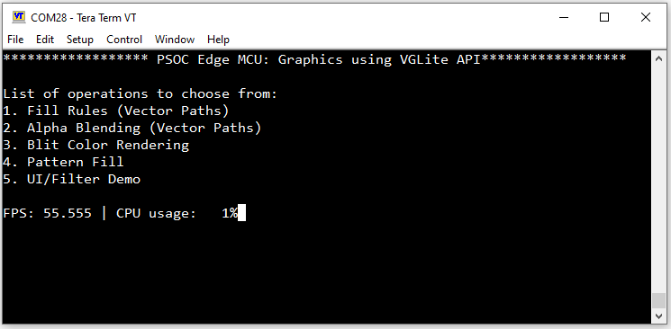
After programming, the application starts automatically. Observe that the UART terminal displays the "
PSOC™ Edge
MCU: Graphics using VGLite API" header, followed by a list of graphical operations that can be selected by the user. See
README.md
file of the application
PSOC™ Edge
MCU: Graphics using VGLite API
for more details. At the end it shows Frame Per Second (FPS) statistic along with CPU usage which is updated regularly as shown in
Figure 17
.
Figure 17.
UART logs on Tera Term
Notice that the Infineon logo is periodically animated on the LCD, as depicted in
Figure 18
.
Figure 18.
Animated image output on LCD

Summary
This application note explains how to get started with the graphics subsystem on
PSOC™ Edge
MCU. It discusses the basic concepts needed for building and programming applications on an embedded MCU. It talks about the hardware and software components of the graphics subsystem. This application note then demonstrates the steps for creating a basic graphics application using ModusToolbox™ and all associated configuration options needed to run the application.
References
Application notes
Code examples
- CE238628: PSOC™ Edge MCU:Graphics using VGLite API
CE239252: PSOC™ Edge MCU: Graphics rendering using CPU vs GPU
CE239540: PSOC™ Edge MCU: Graphics DSI ULPM On Data Lane
CE239259: PSOC™ Edge MCU: Graphics LVGL Demo
CE239203: PSOC™ Edge MCU: Graphics using RLAD
CE239252: PSOC™ Edge MCU: Graphics using single and double buffering
CE238541: PSOC™ Edge MCU: Smartwatch demo using LVGL
Revision history
Document revision | Date | Description of changes |
|---|---|---|
*A | 2025-09-10 | Release to web |
Trademarks
PSOC™, formerly known as PSoC™, is a trademark of Infineon Technologies. Any references to PSoC™ in this document or others shall be deemed to refer to PSOC™.