AN237976 PSOC™ Edge E8 MCU low-power modes and power reduction techniques
About this document
Scope and purpose
This document describes low-power modes in
PSOC™ Edge E8
MCU devices and power management techniques using both hardware and software approaches. This document provides the overview of the different low-power modes available on
PSOC™ Edge E8
MCU to reduce the power consumption and outline specific techniques that optimize the use of MCU features and general power-saving methods. By implementing these techniques, power consumption can be minimized, resulting in a extended battery life. Associated code examples demonstrate different low-power techniques.
Intended audience
This application note is intended for developers who want to learn about the low-power features of the
PSOC™ Edge E8
family devices and general power-saving techniques that can be used to optimize the power consumption and extend the battery life.
Introduction
This application note provides guidelines to developers who can successfully navigate low-power design challenges, optimize power management, and create energy-efficient electronic systems designs using the
PSOC™ Edge E8
MCU.
The following are the main topics explained in this application note:
Understanding the PSOC™ Edge E8 MCU low power modes
Implementing power reduction techniques
Utilizing sleep and wake-up mechanisms
Managing peripheral power
Power supply protection system
Measuring the power consumption
PSOC™ Edge E8 MCU low power features
Power modes
The
PSOC™ Edge E8
MCU product line can operate in five system and three CPU power modes. These modes are intended to minimize the average power consumption in an application. The
PSOC™ Edge E8
MCU supports the following power modes:
Power mode | Description |
|---|---|
System High Performance (HP) |
|
System Low Power (LP) |
|
System Ultra-Low Power (ULP) |
|
CPU Active |
|
CPU Sleep |
|
CPU Deep Sleep |
|
System Deep Sleep 1 |
|
System Hibernate |
|
To achieve System Deep Sleep, you need to configure all related Power Policy Units (PPUs) to either Retention or Off states. Specifically, the PPUs listed in
Table 2
must be set to one of these states to enable System Deep Sleep.
PPU name | Deep sleep mode configuration | Deep Sleep RAM mode configuration | Deep Sleep OFF mode configuration |
|---|---|---|---|
CY_PPU_MAIN_BASE | 0x05 (Full Retention) | 0x02 (Memory Retention) | 0x00 (Off) |
CY_PPU_SRAM0_BASE | 0x02 (Memory Retention) | 0x02 (Memory Retention) | 0x00 (Off) |
CY_PPU_SRAM1_BASE | 0x02 (Memory Retention) | 0x02 (Memory Retention) | 0x00 (Off) |
CY_PPU_SYSCPU_BASE | 0x05 (Full Retention) | 0x00 (Off) | 0x00 (Off) |
CY_PPU_PD1_BASE | 0x05 (Full Retention) | 0x02 (Memory Retention) | 0x00 (Off) |
CY_PPU_APPCPUSS_BASE | 0x05 (Full Retention) | 0x00 (Off) | 0x00 (Off) |
CY_PPU_APPCPU_BASE | 0x05 (Full Retention) | 0x00 (Off) | 0x00 (Off) |
CY_PPU_SOCMEM_BASE | 0x02 (Memory Retention) | 0x02 (Memory Retention) | 0x00 (Off) |
CY_PPU_U55_BASE | 0x00 (Off) | 0x00 (Off) | 0x00 (Off) |
You can use the PPU control APIs from the SysPm PDL library, listed in
Table 3
, to configure and retrieve PPU power modes.
API | Description |
|---|---|
| Sets the required power mode of the particular PPU. |
| Gets the current power mode of the particular PPU. |
| Gets the programmed power mode of the particular PPU. |
Power mode transitions
shows the power mode transitions based on different events and actions, including interrupts, firmware actions, and reset events. In some cases, mode transitions are done through multiple modes. For more detailed information, see the
PSOC™ Edge E8
MCU architecture reference manual and
Power modes summary
.
Figure 1.
PSOC™ Edge E8
MCU device power mode transition
CPU sleep and wake-up instructions
Arm® Cortex® CPU transitions between sleep and wake-up independently.
Figure 2
shows several scenarios of wake-up from sleep.
Wait-for-interrupt (__WFI) is the core sleep instruction. After a CPU executes __WFI, the CPU goes to sleep and stays in sleep until any interrupt is asserted.
Wait-for-event (__WFE) is similar to __WFI, but it wakes up when the wake-up event is received instead of an interrupt. Set Event (__SEV) is used for waking up other CPUs in Sleep mode because of a __WFE.
CPU Deep Sleep uses the same instructions for sleep and wake-up, but the SLEEPDEEP bit[2] of the Arm® System Control Register (SCR) is set before a sleep instruction. For more information on SCR, see the
Arm® system control register user guide
. This process is implemented in the SysPm PDL library.
Figure 2.
Multi-CPU sleep and wake-up scenarios
CPU power modes are different from system power modes.
Figure 2
shows that each CPU supports its own sleep modes, independent of the state of the other CPU. The device is in system Deep Sleep mode when both CPUs are in Deep Sleep.
Subsystem availability in different power modes
Each subsystem resource works differently in various system power modes. For example, the CPU can be in ON, OFF, and Retention modes. It is important to select the proper peripherals for the power mode to work correctly.
Table 4
lists the resources available in different power modes.
Block | Power mode | |||
|---|---|---|---|---|
CPU Active | CPU Sleep | System Deep Sleep | System Hibernate | |
| CPU subsystem | ||||
CPUs | Y | N | N | N |
NPUs | Y | Y | N | N |
NVIC | Y | Y | N | N |
WIC | Y | Y | Y | Y |
RRAM | Y | Y | N | N |
SRAM | Y | Y | Programmable | N |
DMA | Y | Y | N | N |
| Programmable digital | ||||
Smart I/O | Y | Y | Y | N |
| Fixed-function digital | ||||
TCPWM | Y | Y | N | N |
SCB | Y | Y | N, SCB0 is supported in System Deep Sleep power mode | N |
SMIF | Y | Y | N | N |
SD host controller | Y | Y | N | N |
USB | Y | Y | N | N |
CAN FD | Y | Y | N | N |
Ethernet | Y | Y | N | N |
I3C | Y | Y | N | N |
MIPI-DSI | Y | Y | N | N |
TDM/I2S | Y | Y | N | N |
PDM | Y | Y | N | N |
Crypto | Y | Y | N | N |
| Special function | ||||
Graphics subsystem | Y | Y | N | N |
| Programmable analog | ||||
LPComp | Y | Y | Y | Y |
SAR ADC | Y | Y | Y (duty cycled) | N |
DAC | Y | Y | Y | N |
PTComp | Y | Y | Y | N |
CTB | Y | Y | Y | N |
IO | ||||
GPIO | Y | Y | Y | Y |
| System resources | ||||
WDT | Y | Y | Y | Y |
MCWDT | Y | Y | Y | N |
RTC | Y | Y | Y | Y |
Backup registers | Y | Y | Y | Y |
OVD | Y | Y | N | N |
LVD | Y | Y | N | N |
Power supply options
The
PSOC™ Edge E8
MCU product line operates with a single 1.8 V ±5% regulated supply, or from a 2.7 V to 4.8 V supply along with a 1.8 V ± 5% regulated supply.
Supply powered
shows that all other VDDx pins are connected to a 1.8 V source. Isolating analog circuits or separating the rest of the system from noisy GPIOs can be achieved by using isolated sources. Make sure to ground all pins related to VBAT.
Figure 3.
Connection diagram, supply powered
Note:
The bypass capacitors shown in the above diagram are recommendations for typical use only. Actual bypass capacitor usage and size depend on the application.
Battery powered
The battery-powered connection diagram is shown in
Figure 4
. In this configuration, VBAT is connected to a supply that ranges from 2.7 V to 4.8 V. Note that all other VDDx pins must still be connected to 1.8 V, and all '1P8' pins must be grounded. For more information on connection diagram, see the device datasheet.
Figure 4.
Connection diagram, battery powered
Note:
The bypass capacitors shown in the above diagram are recommendations for typical use only. Actual bypass capacitor usage and size depend on the application.
PSOC™ Edge E8 MCU power management
The PSOC™ Edge E8 MCU product line integrates multiple regulators, including an on-chip single-input single-output (SISO) buck converter, to power the blocks within the device in various power modes. The device's various blocks are powered by the regulators, supply pins, and rails depicted in Figure 5 and Figure 6
Figure 5.
Supply powered block diagram
Figure 6.
Battery powered block diagram
Core voltage regulation
Table 5
provides information about the CPU frequency and core voltage for different power modes. It helps understand the relationship between power modes and the corresponding performance characteristics of the CPU.
System power mode | Core voltage (VCCD) | CM33 maximum frequency | CM55 maximum frequency | PDL API function |
|---|---|---|---|---|
System High Performance (HP) | 0.9 V | 200 MHz | 400 MHz | |
System Low Power (LP) | 0.8 V | 80 MHz | 140 MHz | |
System Ultra-Low Power (ULP) | 0.7 V | 50 MHz | 50 MHz | |
System Deep Sleep | 0.7 V | Off | Off | |
System Hibernate | Off | Off | Off | |
Switching (buck) core regulator
The
PSOC™ Edge E8
MCU incorporates a switching (buck) core regulator that functions as a SISO regulator. It regulates the intermediate voltage rail VCCD and all its derivatives, such as VLDO.RET and VCC.SRAM.
In a battery-operated configuration, the system draws current from both VBAT and VDDD. However, in a supply-powered configuration, it completely depends on drawing power from VDDD. It requires a 2.2 μH inductor and a 4.7 μF capacitor to filter the output voltage. This regulator features a high-power low-ripple regulation for System Active mode load currents up to 400 mA and a high-ripple low-power regulation loop for System Deep Sleep mode.
Table 6
lists the Core buck regulator control APIs from the SysPm PDL library that can be used to set the Core Buck Regulator Voltage for the transition between System ULP, LP, and HP power modes.
API | Description |
|---|---|
| Configures the core buck regulator |
| Get the status of core buck regulator |
| Set the core buck regulator mode |
| Get the core buck regulator mode |
| Get the core buck regulator voltage |
| Set the core buck regulator voltage for transition between System ULP, LP, and HP power modes |
Retention LDO
The retention LDO serves the purpose of reducing the Deep Sleep current by supplying lower voltage to retention flops and SRAM cores in System Deep Sleep mode. In System Deep Sleep mode, the retention LDO regulates to provide a nominal voltage of 0.55 V to retention flops and SRAM macros that are in retention across multiple power domains.
It takes the switching regulator output VCCD as its input. The expected maximum load current for the RET LDO is 20 mA. To ensure stability under all RAM use cases for the
PSOC™ Edge E8
MCU, the retention LDO utilizes a 1 μF external capacitor. The amount of retained SRAM is variable and can be selected by the user in 64-KB macros.
Use the following API functions to configure retention LDO and retrieve the status:
API | Description |
|---|---|
| Configures the retention LDO |
| Get the status of retention LDO |
SRAM LDO
During the System ULP mode, the SRAM LDO is responsible for regulating the voltage to facilitate Ultra Low Leakage (ULL) SRAM when VCCD is set at 0.7 V.
In System Active and System Deep Sleep mode, the SRAM LDO is deactivated, and VCCSRAM is directly connected to VCCD through an internal SPST switch. These transitions occur seamlessly and the PMU state machine handles these transitions.
The LDO utilizes an external 1 μF capacitor to ensure stability in all SRAM use cases for the
PSOC™ Edge E8
MCU platform.
API | Description |
|---|---|
| Configures the SRAMLDO regulator |
| Enable/disable the SRAMLDO regulator |
| Set SRAM LDO voltage |
| Get the SRAM LDO voltage |
| Get the status of the RETLDO regulator |
MISC LDO
MISC LDO provides a dedicated analog rail VCCA.DSI for supporting MIPI PHY applications. The “mode” input to the MISC LDO is a static input to the MISC LDO and can only be changed when the MISC LDO is OFF. MISCLDO is OFF in System Deep Sleep and ON in System Active mode. No bypass modes are possible.
API | Description |
|---|---|
| Configures the MISCLDO regulator |
| Get the status of the MISCLDO regulator |
System power management using PDL
Overview
The Peripheral Driver Library (PDL) provides developers with various API functions to optimize power consumption in
PSOC™ Edge E8
MCU by offering low-level control for fine-tuning power-efficient settings.
Developers can optimize power consumption using PDL by selecting specific hardware settings, enabling low-power modes, and efficiently managing peripheral power states.
SysPm (System Power Management)
Within the PDL, the system power management (SysPm) library provides functions to change power modes, as shown in
Figure 1
. The API can also register callback functions to execute a peripheral function before or after power mode transitions.
Use the System Power Management (SysPm) driver to change power modes and reduce system power consumption in power sensitive designs. The functions and other declarations used in this driver are in
cy_syspm.h
. You can include
cy_pdl.h
to get access to all functions and declarations in the PDL. For multi-CPU devices, this library allows you to individually enter low power modes for each CPU.
Operating mode changes for power management
The system supports three active operating modes with corresponding voltage levels:
ULP (Ultra Low Power) – VCCD: 0.7V, VCCSRAM: 0.8V
LP (Low Power) – VCCD: 0.8V, VCCSRAM: 0.8V
HP (High Performance) – VCCD: 0.9V, VCCSRAM: 0.9V
Firmware enables on-the-fly mode transitions, creating a Dynamic Voltage Frequency Scaling (DVFS) system. However, transitions between modes must be carefully managed to prevent timing issues, particularly when adjusting SRAM trims.
Transition frequency requirements
ULP to LP
: Reduce the frequency by at least 18% (e.g., 50 MHz to ≤ 41 MHz) before switching to maintain SRAM timing margin
LP to HP
: Reduce the frequency by at least 38% (e.g., 140 MHz to ≤ 86 MHz) before switching to maintain SRAM timing margin
HP to LP
: Reduce the frequency by at least 82% (e.g., 400 MHz to ≤ 72 MHz) before switching to maintain SRAM timing margin
LP to ULP
: Lower the frequency by at least 66% (e.g., 140 MHz to ≤ 47 MHz) before switching to maintain SRAM timing margin
Switching the System into HP
To set the System HP mode, you need to set the VCCD to 0.9 V. Once you switch into System HP mode, you can increase the operating frequency. To determine the maximum frequency limitations, refer to
Table 5
. To further enhance device performance, you can modify the wait states for memories by calling
Cy_SysLib_SetWaitStates(true, hfClkFreqMz)
, where
hfClkFreqMz
represents the frequency in MHz.
/* Attempt to enter System High Performance (HP) power mode
This function call will transition the system to a higher power mode
to allow for increased clock speeds and performance */

if (CY_SYSPM_SUCCESS != Cy_SysPm_SystemEnterHp())
{
  /* Error handling: device failed to enter System HP mode
  A registered System HP "check ready" callback returned a "not success" status
  Handle the error accordingly, this may include retrying the transition
  or falling back to a lower power mode*/
}
else
{
  /* System successfully transitioned to System HP power mode
  Increase system clock source and adjust peripheral clock dividers as needed
  This can also be done by registering System HP callbacks
  Implement the necessary clock speed changes and adjustments here*/
}
Switching the System into LP and ULP
Before switching into System LP and ULP mode, ensure that the device meets the frequency limitations mentioned in
Table 5
. Decrease the clock frequencies, and slow or disable peripherals. Also ensure that appropriate wait state values are set for the memories by calling
Cy_SysLib_SetWaitStates
.
This code snippet illustrates the transition to System Low Power (LP) mode. To modify it for System Ultra-Low Power (ULP) mode, simply replace the
Cy_SysPm_SystemEnterLp()
function call with
Cy_SysPm_SystemEnterUlp()
.
/* Prepare to enter System Low Power (LP) mode by decreasing clock frequencies, slowing or disabling peripherals, and adjusting peripheral clock dividers as needed. */

if (CY_SYSPM_SUCCESS != Cy_SysPm_SystemEnterLp())
{
  /* Error Handling: The device failed to enter System LP mode.
  A registered System LP "check ready" callback returned a non-success status.
  Handle the error accordingly and take necessary actions.*/
}
else
{
  /* System successfully transitioned to System LP power mode.
  You can now modify the memory wait states as needed.*/
}
Switching the CPU into Sleep
For multi-CPU devices, the
Cy_SysPm_CpuEnterSleep()
function switches the calling CPU into the CPU Sleep power mode. You must clear all pending interrupts before putting the CPU into Sleep mode, even if they are masked.
/* Prepare the system for CPU Sleep mode here.
 * This may include clearing pending interrupts,
 * disabling peripherals, and saving necessary states.
 */

if (CY_SYSPM_SUCCESS != Cy_SysPm_CpuEnterSleep(CY_SYSPM_WAIT_FOR_INTERRUPT))
{
  /* Error: System failed to enter CPU Sleep mode.
  A registered CPU Sleep "check ready" callback returned an error status.*/
}
else
{
  /* System successfully exited CPU Sleep mode.
  The program has resumed execution after waking up from CPU Sleep.*/
}
Switching the System or CPU into Deep Sleep
For multi-CPU devices, the
Cy_SysPm_CpuEnterDeepSleep()
function switches only the CPU that calls the function into the CPU Deep Sleep power mode. To set the whole system into Deep Sleep power mode, ensure that all CPUs call the
Cy_SysPm_CpuEnterDeepSleep()
function.
The CM33_NS application code snippet below demonstrates how to configure the system to enter System Deep Sleep mode, showcasing the necessary steps to achieve System Deep Sleep state.
/*CM33_NS Application*/

/* Enable CM55. CY_CM55_APP_BOOT_ADDR must be updated if CM55 memory layout is changed.*/
Cy_SysEnableCM55(CY_CM55_APP_BOOT_ADDR, CM55_BOOT_WAIT_TIME_USEC);

/* System Domain Idle Power Mode Configuration */
Cy_SysPm_SetDeepSleepMode(CY_SYSPM_MODE_DEEPSLEEP);

/* System SRAM (SoCMEM) Idle Power Mode Configuration */
Cy_SysPm_SetSOCMEMDeepSleepMode(CY_SYSPM_MODE_DEEPSLEEP);

for (;;)
{
  /* Wait for UART traffic to stop */
  while (cy_retarget_io_is_tx_active()) {};

  if (CY_SYSPM_SUCCESS != Cy_SysPm_CpuEnterDeepSleep(CY_SYSPM_WAIT_FOR_INTERRUPT))
  {
    /* Error: System failed to enter CPU Deep Sleep mode.
    A registered CPU Deep Sleep "check ready" callback returned an error status.*/
  }
  else
  {
    /* System successfully exited CPU Deep Sleep mode.
    The program has resumed execution after waking up from CPU Sleep.*/
  }
}
In a similar manner, the CM55 application must also configure its Deep Sleep state and invoke the
Cy_SysPm_CpuEnterDeepSleep
function to enable the system to transition into System Deep Sleep mode.
/*CM55 Application*/

/* Application Domain Idle Power Mode Configuration */
Cy_SysPm_SetDeepSleepMode(CY_SYSPM_MODE_DEEPSLEEP);

for (;;)
{
  /* Put the CPU to deepsleep */
  Cy_SysPm_CpuEnterDeepSleep(CY_SYSPM_WAIT_FOR_INTERRUPT);
}
Note:
The device will not enter System Deep Sleep mode until all related Power Policy Units (PPUs) are set to the correct states, as specified in
Table 2
.
Switching System to Hibernate
If you call
Cy_SysPm_SystemEnterHibernate
from either CPU, the system will be switched into the Hibernate power mode directly because there is no handshake between CPUs.
int main(void)
{
  uint32_t reset_reason;

  /* Get the reset cause */
  reset_reason = Cy_SysLib_GetResetReason();

  if ((reset_reason & CY_SYSLIB_RESET_HIB_WAKEUP))
  {
    Cy_SysPm_IoUnfreeze();
  }

  for (;;)
  {
    Cy_SysPm_ClearHibernateWakeupSource(CY_SYSPM_HIBERNATE_PIN0_LOW);

    /* There is a need to put the device into the system Hibernate modeSetup the
     * Hibernate wakeup source.*/
    Cy_SysPm_SetHibernateWakeupSource(CY_SYSPM_HIBERNATE_PIN0_LOW);

    /* Prepare the device for system Hibernate mode here */
    if (CY_SYSPM_SUCCESS != Cy_SysPm_SystemEnterHibernate())
    {
      /* System did not enter Hibernate mode because a registered
       * Hibernate "check ready" callback returned a "not success" status */
    }
    else
    {
      /* You will never get CY_SYSPM_SUCCESS here because in case of
       * successfully entering system hibernate mode because a wakeup from
       * system Hibernate goes through the system reset.*/
    }
  }
}
The system can wake up from Hibernate mode by configuring the following wake-up sources:
GPIO Wake-up pin
LPCOMP
RTC
WDT
A device-specific pin or pins with programmable polarity can wake up the system. Additionally, certain unregulated peripherals can trigger a wake-up under specific conditions. For instance, a low-power comparator can wake the system by comparing two external voltages. However, it cannot compare an external voltage to an internally generated voltage. The Watchdog Timer (WDT) can also be configured to wake up the system by generating a WDT interrupt.
Note:
When booting from System Hibernate mode, store the CM33 secure application in RRAM. Then, call the
Cy_SysPm_IoUnfreeze()
function to unfreeze the GPIOs, which are frozen when the device enters System Hibernate mode, and configure the SMIF. For a more detailed explanation on booting the application from RRAM, refer to application note AN239774: Selecting and configuring memories for power and performance in
PSOC™ Edge E8
MCU.
SysClk (System Clock)
The System Clock (SysClk) driver provides API functions that configure system and peripheral clocks. The
cy_sysclk.h
header file contains the necessary functions and declarations for this driver. By including
cy_pdl.h
, you can access all functions and declarations in the PDL.
Use the API functions to configure, enable, or disable a clock. The clock system includes a variety of resources that can vary per device, including:
Internal clock sources, such as internal oscillators
External clock sources, such as crystal oscillators or a signal on an I/O pin
Generated clocks, such as a DPLL, and peripheral clocks
Update the DPLL frequency
The DPLLs provide fast wake-up at high clock speeds. There are two types of DPLL :
Two lower frequency and optimized for low power (DPLL LP)
One high-frequency and high-performance (DPLL HP)
The HP DPLL is optimized for high-speed operation and can operate across a frequency range of 50 MHz to 500 MHz. The LP DPLL, on the other hand, operates across a broad range of frequency from 10 MHz to 500 MHz. Prefer LP DPLL over HP DPLL to minimize power consumption in power-sensitive applications.
Before updating the DPLL frequency, disable the DPLL if it changes the input frequency. After calling this function, configure the DPLL using
Cy_SysClk_PllConfigure()
as shown below:
void dpll_lp_set_freq(uint32_t freq)
{
    /* Define DPLL config structure */
    cy_stc_pll_config_t dpll_lp;

    /* Set DPLL input frequency */
    dpll_lp.inputFreq = DPLL_INTPUT_FREQ_HZ;

    /* Set DPLL output mode to auto */
    dpll_lp.outputMode = CY_SYSCLK_FLLPLL_OUTPUT_AUTO;

    /* Set desired DPLL output frequency */
    dpll_lp.outputFreq = freq;

    /* Disable DPLL_LP_0 PLL path */
    Cy_SysClk_PllDisable(SRSS_DPLL_LP_0_PATH_NUM);

    /* Configure DPLL with specified settings */
    if (CY_SYSCLK_SUCCESS !=
        Cy_SysClk_PllConfigure(SRSS_DPLL_LP_0_PATH_NUM, &dpll_lp))
    {
        /* If config fails, assert error */
        CY_ASSERT(0);
    }

    /* Enable DPLL_LP_0 PLL path with timeout */
    if (CY_SYSCLK_SUCCESS !=
           Cy_SysClk_PllEnable(SRSS_DPLL_LP_0_PATH_NUM, DPLL_ENABLE_TIMEOUT_MS))
    {
        /* If enable fails, assert error */
        CY_ASSERT(0);
    }
}
If this function affects the CLK_HF0 frequency, then follow these steps:
Update the system core clock by calling
SystemCoreClockUpdate()
If the frequency is increasing, call
Cy_SysLib_SetWaitStates()
before calling this function
If the frequency is decreasing, call
Cy_SysLib_SetWaitStates()
after calling this function
HF Clock enable and frequency check:
#define HFCLK1 (1UL)

uint32_t clkHf1freq;

if (Cy_SysClk_ClkHfIsEnabled(HFCLK1))
{
    /* Check the HFCLK0 frequency */
    clkHf1freq = Cy_SysClk_ClkHfGetFrequency(HFCLK1);
}
Allocate a clock to a peripheral:
Configure an 8-bit prescaler to divide the clock frequency for a specific TCPWM block.
#define PERI_DIV  (32)
#define DIVIDER_NUM (1U)


/* Disable the 8-bit divider #1 */
Cy_SysClk_PeriphDisableDivider(CY_SYSCLK_DIV_8_BIT, divider_num);

/* Assign 8-bit divider #1 to source TCPWM0 CNT0 clock */
Cy_SysClk_PeriphAssignDivider(PCLK_TCPWM0_CLOCKS0, CY_SYSCLK_DIV_8_BIT, 1UL);

/* Set the 8-bit divider #1 value to 32 */
Cy_SysClk_PeriphSetDivider(CY_SYSCLK_DIV_8_BIT, divider_num, peri_div);

/* Enable the 8-bit divider #1 */
Cy_SysClk_PeriphEnableDivider(CY_SYSCLK_DIV_8_BIT, divider_num);
Change clock source
Configure the HF2 clock to use the External Crystal Oscillator (ECO) as its clock source.
#define CLKPATH2 (2UL)
#define HFCLK2 (2UL)

/* Configure clock path 2 to use the External Crystal Oscillator (ECO) as its source */
Cy_SysClk_ClkPathSetSource(CLKPATH2, CY_SYSCLK_CLKPATH_IN_ECO);

/* Set the source of HFCLK2 to clock path 2, which is now driven by the ECO */
Cy_SysClk_ClkHfSetSource(HFCLK2, CY_SYSCLK_CLKHF_IN_CLKPATH2);

/* Enable the HFCLK2 clock, which is now sourced from the ECO via clock path 2 */
Cy_SysClk_ClkHfEnable(HFCLK2);
Mode transition functions
The SysPm driver handles low-power callbacks declared in the application. If there are no callbacks registered, the device executes the power mode transition. However, frequently your application firmware must make modifications for low power mode. For example, you may need to disable a peripheral or ensure that a message is not being transmitted or received.
To enable this, the SysPm driver implements a callback mechanism. When a lower power mode transition is about to take place (either entering or exiting System Power Modes), the registered callbacks for that transition are called. Every callback function should handle the four possible steps shown in
Table 10
Callback function option | Description |
|---|---|
| Checks the ready state to transition to other mode. Exits without transition if it returns . |
| Callbacks execute and configure required actions before mode transition. |
| Callbacks execute after mode transition or configuration. |
| Callbacks execute only when fails. It executes the rollback action. |
A callback function can skip steps.
Table 11
outlines the available skip options.
Callback function skip option | Description |
|---|---|
| Define to skip check ready mode in the SysPm callback. |
| Define to skip check fail mode in the SysPm callback. |
| Define to skip before transition mode in the SysPm callback. |
| Define to skip after transition mode in the SysPm callback. |
The SysPm driver organizes all the callbacks into a linked list. While entering a low power mode, SysPm goes through that linked list from first to last, executing the callbacks one after another. While exiting low power mode, SysPm goes through that linked list again, but in the opposite direction from last to first. This ordering supports prioritization of callbacks relative to the transition event.
Best practices for low-power design
Turning Off PD1 domain
Figure 7.
PSOC™ Edge E8
power domains
The
PSOC™ Edge E8
features two power domains as shown in
Figure 7
. The always-on low-power domain (PD0) and the high-performance domain (PD1). Both domains are powered by the internal buck output. Both PD1 and PD0 domains operate at the same voltage.
Additionally, PD1 can be independently turned off, while PD0 remains on unless the chip power is removed. For applications that do not require high-performance peripherals in the PD1 domain, the domain can be completely turned off to conserve power and brought up again as needed.
The following code snippet demonstrates how to disable the PD1 domain:
Code snippet of CM33_NS project:
#define WAIT_FOR_CM55_EXE             (300U)

/* Disable the System SRAM (SoCMEM) to reduce power consumption */
Cy_SysEnableSOCMEM(false);

/* Disable SMIF (Serial Memory Interface) Core 0 to prevent any ongoing transactions */
Cy_SMIF_Disable(SMIF0_CORE0);

/* De-initialize SMIF Core 0 to release any allocated resources */
Cy_SMIF_DeInit(SMIF0_CORE0);

 /* Set idle power mode configuration of System SRAM (SOCMEM) to deepsleep */   Cy_SysPm_SetSOCMEMDeepSleepMode(CY_SYSPM_MODE_DEEPSLEEP);

/* Set deepsleep mode to deepsleep off */     Cy_SysPm_SetDeepSleepMode(CY_SYSPM_MODE_DEEPSLEEP_OFF);

/* Clear APPCPUSS and SYSCPU power domain dependency */
 (void)cy_pd_pdcm_clear_dependency(CY_PD_PDCM_APPCPUSS , CY_PD_PDCM_SYSCPU);

/* Disable PD1 power*/
(void)cy_pd_ppu_set_power_mode((struct ppu_v1_reg *)CY_PPU_PD1_BASE, (uint32_t)PPU_V1_MODE_OFF);

/* Disable SoCMEM power */
(void)cy_pd_ppu_set_power_mode((struct ppu_v1_reg *)CY_PPU_SOCMEM_BASE, (uint32_t)PPU_V1_MODE_OFF);

/* Disable APPCPUSS power */
(void)cy_pd_ppu_set_power_mode((struct ppu_v1_reg *)CY_PPU_APPCPUSS_BASE, (uint32_t)PPU_V1_MODE_OFF);

/* Disable APPCPU(CM55) power */
(void)cy_pd_ppu_set_power_mode((struct ppu_v1_reg *)CY_PPU_APPCPU_BASE, (uint32_t)PPU_V1_MODE_OFF);

/* Code to enable CM55 */

/* Wait for CM55 execution */
Cy_SysLib_Delay(WAIT_FOR_CM55_EXE);

/* Disable HF1 and HF2 clocks */
Cy_SysClk_ClkHfDisable(CY_CFG_SYSCLK_CLKHF1);
Cy_SysClk_ClkHfDisable(CY_CFG_SYSCLK_CLKHF2);
Code snippet of CM55 project:
#define DEEP_SLEEP_OFF_TOKEN  (0xB1)

/* Set deepsleep mode to deepsleep off */
Cy_SysPm_SetDeepSleepMode(CY_SYSPM_DEEPSLEEP_OFF);
    for (;;)
    {

     SRSS_PWR_HIBERNATE= | (SRSS_PWR_HIBERNATE  | DEEP_SLEEP_OFF_TOKEN);
        Cy_SysPm_CpuEnterDeepSleep(CY_SYSPM_WAIT_FOR_INTERRUPT);

    }
To disable PD1 (Power Domain 1) , move all three projects to the internal memory (For example RRAM) as SMIF needs to be disabled for PD1 to be disabled. Detailed steps for code and data movement across memories are covered in the application note AN239774: Selecting and configuring memories for power and performance in
PSOC™ Edge E8
MCU.
Disabling CPUs
If the CM55 CPU is not used in the application, disable it by calling the
Cy_SysDisableCM55()
function from the CM33 firmware. You can also set the
Clk_Fast
divider to 256 to minimize any fan-out leakage from this clock. If the CM33 CPU is not used in the application, place it in System Deep Sleep power mode and set the
Clk_Slow
divider to 256 to minimize any fan-out leakage from this clock.
Clocks
Running the CPU clock faster can help lower the
PSOC™ Edge E8
MCU's average current consumption. This can be achieved by completing tasks or computations faster, which will reduce the time the device spends in CPU Active mode and increasing its duration in CPU Sleep or System Deep Sleep mode.
Although some tasks, such as sensor reading and data transmission, require the same amount of time, others, such as data processing, require less time when the CPU operates at a faster frequency. However, there is a point where the energy required to drive the clocks at a higher rate overcomes the benefit of a shorter active time.
Figure 8.
Current profile example
suggests 200 MHz as the optimal speed. With a 200 MHz clock, the time spent in Active mode is about half that spent with a 50 MHz clock, despite the peak current consumption being greater. Ultimately, running the CPU as fast as possible to complete processing and spending more time in low-power mode is the best approach for
PSOC™ Edge E8
devices.
To reduce power consumption further for an application, you should disable all unused clock sources. Different peripherals require different frequencies, leading to the use of multiple clock sources. Enabling more clock sources increases power consumption.
Periodic wake-up timers
A periodic wake-up from the CPU Sleep mode is the most common way to reduce power consumption. The ratio of CPU active period power consumption to CPU sleep period power consumption determines the average power consumption. To achieve the best result, the sleep period should be as long as possible, and the active period should be as short as possible.
The WDT and MCWDT are effective periodic wake-up sources in System Deep Sleep and System Hibernate modes. If the application needs longer or more precise wake-up periods, an RTC alarm can be a good periodic wake-up source.
Figure 9.
Average power consumption
Tickless timer in FreeRTOS
Tickless idle mode in FreeRTOS reduces power consumption by minimizing CPU wake-ups, customizing low-power configurations, optimizing task scheduling, and providing the means to monitor and improve power efficiency during idle periods, which is crucial for battery-powered or energy-efficient applications.
Do the following to achieve low power consumption in FreeRTOS with tickless idle mode in the
PSOC™ Edge E8
MCU:
Configure FreeRTOS to enable the tickless idle mode by setting the
configUSE_TICKLESS_IDLE
macro to '2' in the
FreeRTOSConfig.h
file
In application code, use FreeRTOS API functions such as
vTaskDelayUntil()
or
vTaskDelay()
instead of busy-wait loops to introduce idle time in tasks. This allows the tickless idle mode to kick in effectively. Additionally, adjust the FreeRTOS tick rate to match the respective application's requirements to minimize wake-ups
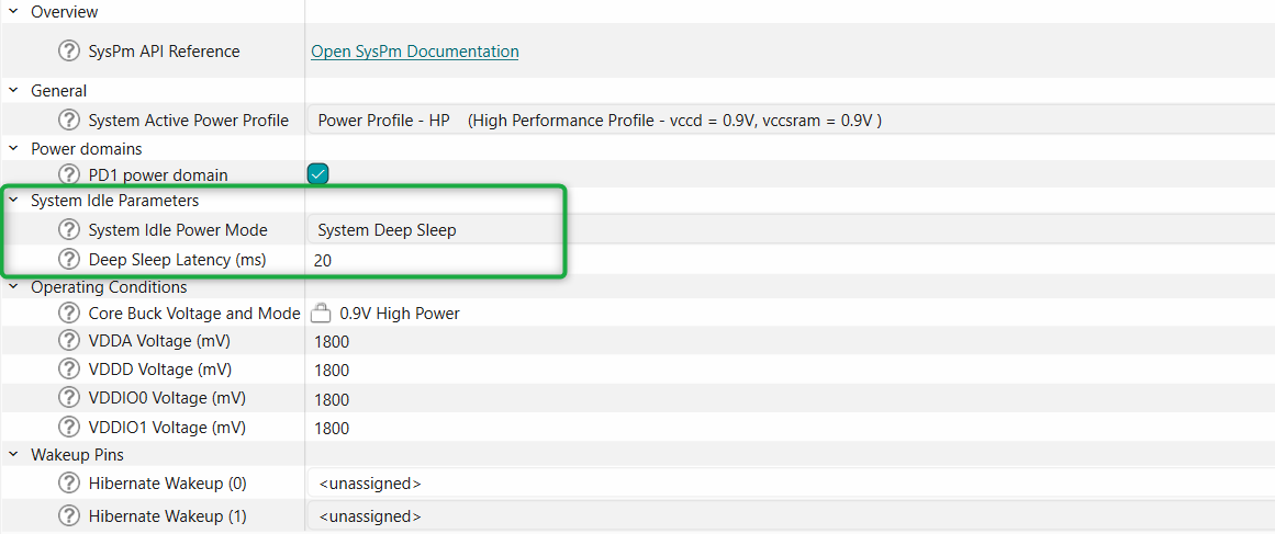
Update the
System Idle Parameters
in the Device Configurator as shown below:
Figure 10.
Tickless Idle configuration
Use DMA to move data
You can save power any time you offload a task from the CPU and either halt the CPU or let it do something else in parallel. The DMA engine can be used in both system LP and ULP modes to transfer data with no CPU use. The power saved is either the difference between CPU active and CPU stop power modes if the CPU can be halted or a lower CPU active current if the CPU can be clocked at a slower frequency and still get the same work done.
Splitting tasks between the CPUs
The following are a few of the several reasons to choose either CM55 or CM33 to do certain tasks:
Tasks that require computation-heavy operations are more efficiently run on CM55
Tasks that are time-critical and require the maximum clock speed (400 MHz) should run only on CM55
Identify the tasks that require less computational power and can be executed on the CM33 core. These could be tasks such as sensor data processing, data filtering, or controlling peripherals
When maximizing the system idle state time as discussed in the
Clocks
section, it may be beneficial to spread tasks between CM33 and CM55 so that the lower-power idle state can be entered faster due to simultaneous task processing
If single CPU processing must be spread out over a long period due to real-time hardware interactions that limit time spent in lower-power states, CM33 will often be lower-power than CM55 over the same active time interval
If processing power is required that exceeds what one CPU can provide, the tasks should be spread between both cores. Because each core has its own bus controller and can access separate memory blocks, there are minimal wait states due to bus or memory contention. The performance decrease due to contention is typically less than 2%, while the performance increase from the second core is greater than 50% (assuming CM33 is added to CM55)
In applications that stay in active mode and can achieve the required processing power on a single core, There is most often no power benefit to sharing the required tasks between cores
Use GPIOs to gate current paths
PCBs may contain other components that draw power; MCUs can be used to control the power through them by supplying the power with GPIO pins that can be turned ON and OFF in firmware. If a higher current is required than the GPIO can directly supply, use external power devices that are controlled by the GPIO.
Note:
The maximum pin source and sink capabilities listed in the data sheet must not be exceeded.
A good example of this scenario is a low-power comparator (LPComp) application, as shown in
Figure 11
.
In this case, the device compares the voltage on an analog pin, which changes as the potentiometer resistance changes. LPComp can be turned OFF when not in use, but external components will still consume power because the current path through the resistor and potentiometer remains. A simple solution with the MCU is to use a second pin as a switch to ground, as shown in
Figure 11
.
Figure 11.
Typical LPComp application
In this configuration, the current flow can be stopped by writing a ‘1’ to Pin_3 and allowing the pin to float. This removes the current consumption by reducing the voltage differential across the two resistors to 0 V. Writing a ‘0’ resumes the current flow. Only one pin and a few lines of code are required to implement this power-saving feature.
Disable unused peripherals and clocks
You can achieve a significant reduction in current consumption by disabling unused blocks, with the amount of power saved varying depending on the specific block you disable. Additionally, if you do not use the high-frequency clock roots in your application, consider disabling them either from the device configurator or programmatically, as shown in the code snippet.
/* Wait until the UART transmission is complete */
while(!Cy_SCB_IsTxComplete(UART_HW)){}

/* Disable the UART module */
Cy_SCB_UART_Disable(UART_HW, &uart_ctx);

/* Disable the high-frequency clock for the UART peripheral */
Cy_SysClk_ClkHfDisable(10);
GPIOs
GPIOs can continue to drive external circuitry while the
PSOC™ Edge E8
MCU is in any low-power mode. This is helpful when you need to hold external logic at a fixed level, but it can lead to wasted power if the pins needlessly source or sink current. The specific power savings of this technique depend on the circuit attached to the specific GPIO pin.
SRAM
PSOC™ Edge E8
MCU devices allow powering off individual SRAM banks or pages within a bank. The size of pages within a bank depends on the specific device and bank, as detailed in the device data-sheet. Specific devices will have one or more SRAM banks. Most devices have one bank with a smaller page size (typically 64 KB) for fine-grained control of the amount of SRAM enabled.
Disable any unused page by using
Cy_SysPm_SetSRAMMacroPwrMode
API function. This technique is particularly effective in System Deep Sleep mode, where it helps reduce the current consumption of unused SRAM blocks.
/*Set Power mode of MACRO_1 in a SRAM0 to off*/
Cy_SysPm_SetSRAMMacroPwrMode(CY_SYSPM_SRAM0_MEMORY, CY_SYSPM_SRAM0_MACRO_1, CY_SYSPM_SRAM_PWR_MODE_OFF);
Running code on internal SRAM can be more power-efficient than running it on external flash. For more information on how to run code from various internal and external memories, refer to application note
AN239774: Selecting and configuring memories for power and performance in
PSOC™ Edge E8
MCU.
System SRAM (SoCMEM)
To minimize power consumption, you can selectively turn off blocks of System SRAM in 512 KB increments. The System SRAM controller provides programmable wait states, ranging from 0 to 3, which allow you to fine-tune its performance. Specifically, you can configure these wait states by programming the CTL.SRAM_WS[1:0] bits.
/*Disable power to SoCMEM Partition 0 in Deep Sleep mode to reduce power consumption*/
Cy_SysPm_SetSOCMemPartDsPwrMode(CY_SYSPM_SOCMEM_SRAM_PARTITION0, CY_SYSPM_SOCMEM_SRAM_DS_MODE_RET_OFF);
TCPWM
When using a counter, timer, or PWM, you should configure the clock to source the channel as low as possible while still meeting the frequency and accuracy requirements. For example, if you need to generate a 1-second interrupt with a timer, it is better to use a clock frequency of 1 kHz with a period equal to 1,000 counts than a clock frequency of 1 MHz with a period equal to 1,000,000 counts. The power savings from reducing the TCPWM clocks are mostly linear based on clock frequency. TCPWM operating current at 100 MHz = 540 µA (SID.TCPWM.2B) while at 8 MHz = 70 µA (SID.TCPWM.1) per the
PSOC™ Edge E8
datasheet.
SCB
Avoid using blocking functions when sending or receiving data. Use interrupt-based events or an RTOS to transfer the data while yielding the CPU to other tasks so that the CPU is in a Sleep state for a longer duration instead of polling the status of the transmission.
Figure 12
shows an example of blocking and non-blocking functions.
Figure 12.
Example of blocking and non-blocking functions
Instead of using the SCB interrupt to access its FIFO in firmware, use DMA controlled by the FIFO level to reduce the number of CPU cycles required in the application; therefore, the CPU can stay in a Sleep state longer or execute other tasks. If the SCB block uses any pin connections, set the pins to analog High-Z when the block is disabled.
To reduce power consumption, operate the system at the lowest possible data rate because the SCB's power increases linearly with clock frequency. Additionally, ensure that all bits are transmitted before disabling it.
I2S
The I2S peripherals can be put in idle mode to save power consumption. This is achieved by gating the system clock to the I2S peripherals via individual fields in the Peripheral Clock Gating Configuration registers described in the reference manual.
I3C
Due to a change in output method from an open drain method to a push-pull output, I3C can be much more energy efficient than I2C. An open-drain process requires pull-up resistors that, when activated, require a significant amount of power to operate. Push-pull operations do not require pull-up resistors to work, meaning the method can reduce energy consumption because it does not need to power any external resistors to function.
Another factor that plays into the power-saving quality of I3C over I2C is its data transfer speed improvements. The benefits here are simple to understand. Because messages can now be sent over the I3C bus at significantly faster rates, the bus can turn on and shut off target devices much quicker than was possible with I2C. This process saves a noticeable amount of power consumption compared to I2C.
ADC
When selecting the pins to be connected to the SAR ADC, preferably choose the dedicated port connected to the SAR MUX first. Only after running out of pins in that port, choose pins from other ports. By only using the dedicated port, there is no need to use the global analog muxes, which consume extra current.
You can also achieve higher sample rates with the dedicated port due to the lower input capacitance. If the full-rated accuracy of ADC results is not required, use a lower resolution and do not use averaging, which reduces the number of ADC clocks required for the same sample rate.
If the maximum sample rate is not required, consider using the single-shot mode instead of continuous mode. This avoids the SAR ADC operating all the time. In single-shot mode, the ADC samples only when triggered by software or hardware, depending on the application.
If the main application is not required to perform processing during ADC sampling, the
PSOC™ Edge E8
MCU family of devices supports the operation of SAR ADC in System Deep Sleep power mode, enabling you to power down the CPUs while collecting data.
DAC
If the DAC voltage output needs to be periodically changed with per-determined values, use a DMA to update the voltage value. This avoids using CPU cycles to write to DAC registers. If the external device that requires the DAC output voltage is used only periodically, keep the DAC disabled when its output is not required. When the DAC output voltage must be provided while in system deep sleep, use a “sample-and-hold” strategy to maintain the voltage output while the voltage DAC is disabled in system deep sleep.
Opamp
The
PSOC™ Edge E8
MCU product line has two blocks, each with two independent opamps, for a total of four opamps. The opamp outputs go to device pins as well as being able to drive internal nodes, but not simultaneously. Depending on the use case, a power mode choice can be made in order to reduce power consumption.
Inter Processor Communication (IPC)
PSOC™ Edge E8
MCU incorporates two Inter Processor Communication (IPC) blocks namely IPC0 in low-power domain and IPC1 in high-performance domain.
IPCs are not system deep sleep capable however IPC can wake-up other CPU from deep sleep. IPC0 can wake-up high-performance CPU subsystem whereas IPC1 can wake-up low-power CPU subsystem from CPU deep sleep.
Each IPC instance includes 16 channels and 8 interrupt structures. The IPC channels can be used for communication and synchronization between CPUs. Each IPC channel also implements a locking scheme which can be used to manage shared resources. The IPC interrupts let one CPU interrupt the other, signaling an event. This is used to trigger events such as notify and release of the corresponding IPC channels. One IPC0 channel is reserved for Secured Enclave.
SDHC
Use the following guidelines to optimize the power consumption for the SDHC peripheral:
Reduce the clock frequency to the lowest acceptable value while still meeting the SDHC card's timing requirements. Lower clock speeds consume less power
Utilize the low-power modes available in your MCU. These modes can reduce power consumption significantly when the MCU is not actively communicating with the SDHC card. Common low-power modes include Sleep, Standby, and Hibernate
Only activate and power the SDHC peripheral when needed. Deactivate it during idle times to minimize power consumption
Disable any SDHC card features or modes that are not required for your application. For example, if you do not need write protection, disable it to save power
Audio subsystem
When you design audio and voice applications, you need to think about power consumption. Most of the time, you want to minimize power consumption. This is especially important when you need your device to always be listening for audio, like with voice assistants. To make this work while saving power, you can use a three-level architecture, as shown in
Figure 13
.
Figure 13.
Three-level architecture for Always-On audio applications
In the first level of this architecture, you use the analog microphone with the LPASS subsystem, which runs on low power and can stay ON even when the system is in Deep Sleep. When the LPASS detects a sound, it wakes up the low-power core. The core, specifically the CM33 core, then uses the Speech Onset Detection (SOD) algorithm to determine if the sound is actually someone speaking. If it is, the audio data is sent to the next level, which is the Low Power Wake Word Detection (LPWWD).
The second level of this architecture is where the Speech Onset Detection (SOD) and Low Power Wake Word Detection (LPWWD) occur. This is where the system checks if the sound detected is actually a human voice and a wake word.
The third level is where the High Performance Wake Word Detection (HPWWD) takes place. By breaking it down into these three levels, you can make sure that the high-performance core (CM55) only wakes up when it is really needed, which helps save a lot of power.
To save as much power as possible, you can take a few important steps. First, using an analog microphone with the LPPASS can help reduce power consumption. Second, turning off the Power Domain 1 (PD1) can also help save power since the HPWWD is the third level of low-power voice applications. Additionally, you can take a few more steps to minimize power consumption. Using the U55 core for HPWWD is a good idea, as it can process information faster than the CM55 core.
Clock Generation for audio Interfaces
: A high-frequency clock generated from the DPLL sources the I2S and PDM/PCM blocks. For high-accuracy frame rates, an ECO sources the DPLL. When picking a frequency for the ECO, consider the following desired audio sample rates:
To support all standard audio sample rates (8/16/22.05/32/44.1/48 kHz), the required minimum ECO frequency is 17.2032 MHz
To support only the sample rates of 8/16/48 kHz, configure the DPLL for 12.288 MHz
To support only the sample rates of 22.05/44.1 kHz, configure the DPLL for 22.5792 MHz
When the audio subsystem is not in use, make sure to turn off the I2S and/or PDM/PCM blocks to save power. Do not forget to also disable the related DPLL and any other unused clock paths, as these can be a major source of high power consumption.
Graphics subsystem
Use the following guidelines to optimize the power consumption for graphics subsystem:
Adjust the frame rate dynamically based on the content being displayed. Lowering the frame rate when displaying static or less complex graphics can significantly reduce power consumption
Implement adaptive backlight control based on the ambient light sensor data. Dim the backlight when operating in low-light conditions or when the screen's content allows it
Implement screen dimming or sleep modes during inactive state. This can involve turning off or reducing the power to the MIPI DSI and graphics engine
Minimize the area of the screen that needs to be updated. Implement partial screen updates instead of refreshing the entire display, especially in applications where only specific regions of the screen change frequently
If supported by the MCU and display, use frame buffer compression techniques to reduce the memory bandwidth and power consumption during screen updates
Investigate the support for low-power display modes, such as MIPI DSI's Low Power state (LP mode). In this mode, the display can reduce its power consumption when there is no content to display
Power supply protection system
The
PSOC™ Edge E8
MCU offers multiple voltage monitoring and supply failure protection options. This includes BOD and LVD. Adjusting threshold levels to lower values and disabling any unused monitoring or protection features on the MCU can effectively reduce power consumption by minimizing unnecessary activation and ensuring that protection systems trigger only when needed.
Brownout detect (BOD)
A brownout detector (BOD) can reset the system before the logic state is lost when VDDD and VCCD power are lost. The brownout system guarantees a reset before VDDD reaches the minimum system operating voltage, and works for all logic, SRAM, and RRAM. BOD is controlled by hardware; there is no configurable register. For details on the BOD trip points, supported supply ramp rate, and BOD detector response time, refer to the device datasheet.
Low-voltage detect (LVD)
An LVD circuit monitors the external supply voltage and generates an interrupt or fault while the device is still within its operating limits. Firmware can utilize the LVD interrupt to implement proactive measures for prevention.
The
PSOC™ Edge E8
MCU incorporates a single LVD on the VBAT rail. It is active and functional during both the CPU Active and CPU Sleep modes. In System Deep Sleep mode, the LVD can be enabled to wake up the system by triggering an interrupt, but it does not operate during System Hibernate mode. By default, the LVD is disabled to conserve power because its operation consumes energy. The following code snippet shows how to configure LVD using PDL API functions.
/* Disable LVD interrupts */
Cy_LVD_ClearInterruptMask();

/* Set the threshold value for monitoring the VDDD voltage */
Cy_LVD_SetThreshold(CY_LVD_THRESHOLD_2_75_V) ;

/* Set configuration for LVD interrupt */
Cy_LVD_SetInterruptConfig(CY_LVD_INTR_BOTH);

/* Enable the LVD Block */
Cy_LVD_Enable();

/* Provide delay to avoid false interrupt detection */
Cy_SysLib_DelayUs(20U);

/* Clear any false interrupt */
Cy_LVD_ClearInterrupt();

/* Initialize the LVD interrupt */
(void)Cy_SysInt_Init(&lvd_interrupt_cfg, lvd_interrupt_handler);

/* Enables LVD interrupts */
Cy_LVD_SetInterruptMask();
NVIC_EnableIRQ(lvd_interrupt_cfg.intrSrc);
Power measurement
Measuring the current with a DMM
When using a digital multimeter (DMM) to measure device current, notice the value of the shunt resistor in the DMM. DMMs have one or more (shunt) resistors between the current inputs. These resistors can range from less than an ohm to more than 10 kΩ. There is no standard value for the shunt resistor between brands or even models from the same vendor. Review the meter’s manual and learn the value of the shunt resistor because there will always be a voltage drop across this shunt. This means that the
PSOC™ Edge E8
device will not see the same supplying voltage. For example, if the shunt resistor in the meter is 1 Ω or less, there is only a few millivolts drop when measuring the MCU current, which can be ignored. If the shunt resistor is 1 kΩ, a 1 mA current results in a 1 V drop.
High shunt resistor values can cause the device to reset because of low voltage at higher currents. Additionally, when changing ranges, make sure that the DMM does not do a “break-before-make”, or the power will be cycled and the project will be reset.
For extremely low currents in deep sleep, hibernate, and stop modes, a good technique is to use a zero or low resistance shunt until the device enters low-power mode. After entering low-power mode, the code should keep the device in that mode and switch to a high-resistance shunt for current measurement. As an alternative to relying on the DMM shunt, most
PSOC™ Edge E8
MCU kits include a place for a shunt resistor or current measurement header.
See the respective kits user guide to determine specific current measurement features. These can be replaced or connected to a small resistor allowing voltage measurement across the shunt with a voltmeter, and then determine the current. A shunt resistance between 1 Ω and 100 Ω should work well for most applications.
Approximating the power consumption
The device datasheet provides information to estimate the
PSOC™ Edge E8
MCU power consumption for project-specific user configurations.
Additionally you can use
PSOC Edge E8 MCU: Power measurements
code example to configure and measure various datasheet parameters.
Power modes summary
Power modes and wake-up source
System power mode | CPU power mode | Description | Entry conditions | Wake-up sources | Wake-up action |
|---|---|---|---|---|---|
System High Performance (HP) | Active | 0.9 V core voltage. All peripherals are available (programmable). Maximum clock frequencies possible. | Manual register write from system LP mode. Wake-up from CPU Sleep or CPU Deep Sleep while in system HP mode. Wake-up from System Deep Sleep after entering from HP mode. | NA | NA |
Sleep | 0.9 V core voltage. One or more CPU in Sleep mode (execution halted). All peripherals are available (programmable). | CPU executes WFI/WFE instruction with Deep Sleep disabled | Any interrupt to CPU | Interrupt | |
Deep Sleep | 0.9 V core voltage. One CPU in Deep Sleep mode (execution halted). Other CPU in Active or Sleep mode. All peripherals are available (programmable). | CPU executes WFI/WFE instruction with Deep Sleep enabled | Any interrupt to CPU | Interrupt | |
System Low Power (LP) | Active | 0.8 V core voltage. All peripherals are available (programmable) Reduced clock frequencies | Reset from external reset, brownout, power-on reset system and Hibernate mode. Manual register write from system HP or ULP mode. Wake-up from CPU Sleep or CPU Deep Sleep while in system LP mode. Wake-up from system Deep Sleep after entering from LP mode | NA | NA |
Sleep | 0.8 V core voltage. One or more CPU in Sleep mode (execution halted). All peripherals are available (programmable) | CPU executes WFI/WFE instruction with Deep Sleep disabled | Any interrupt to CPU | Interrupt | |
Deep Sleep | 0.8 V core voltage. One CPU in Deep Sleep mode (execution halted). Other CPU in Active or Sleep mode. All peripherals are available (programmable) | CPU executes WFI/WFE instruction with Deep Sleep enabled | Any interrupt to CPU | Interrupt | |
System Ultra-Low Power (ULP) | Active | 0.7 V core voltage. All peripherals are available (programmable). Reduced clock frequencies. | Manual register write from system LP mode. Wake-up from CPU Sleep or CPU Deep Sleep while in system ULP mode. Wake-up from system Deep Sleep after entering from ULP mode | NA | NA |
Sleep | 0.7 V core voltage. One or more CPU in Sleep mode (execution halted). All peripherals are available (programmable) | CPU executes WFI/WFE instruction with Deep Sleep disabled | Any interrupt to CPU | Interrupt | |
Deep Sleep | 0.7 V core voltage. One CPU in Deep Sleep mode (execution halted). Other CPU in Active or Sleep mode. All peripherals are available (programmable) | CPU executes WFI/WFE instruction with Deep Sleep enabled | Any interrupt to CPU | Interrupt | |
System Deep Sleep | Deep Sleep | 0.7 V core voltage. All high-frequency clocks and peripherals are turned off. SRAM is retained (programmable). | Both CPUs simultaneously in CPU Deep Sleep mode | GPIO interrupt, Autonomous Analog, Low-Power comparator, SCB, watchdog timer, and RTC alarms | Interrupt/Partial reset |
System Hibernate | NA | GPIO states are frozen. All peripherals and clocks in the device are completely turned off except optional low-power comparators and backup domain | Manual register write from HP, LP, or ULP modes | WAKEUP pin, low- power comparator, watchdog timer, and RTC alarms | Reset |
Subsystem availability
Power mode support
CPU Active/Sleep | System Deep Sleep | System Deep sleep-RAM | System Deep sleep-Off | System Hibernate | Off | |
|---|---|---|---|---|---|---|
Parameters | ||||||
Wake source | Any interrupt | DS peripherals | DS peripherals | DS peripherals | RTC/HIB peripherals | Power on |
Wake action | Resume | Resume | Warm boot | Reset/cold boot | Reset | Reset |
Wake time | 1 CPU cycle | < 20 μs | Deep sleep+warm boot | Deep sleep+cold boot | POR + cold boot | NA |
Resources | ||||||
IHO | On | Off | Off | Off | Off | Off |
PILO | On/Off | On/Off | On/Off | On/Off | On/Off | Off |
ECO | On/Off | Off | On/Off | On/Off | Off | Off |
WCO | On/Off | On/Off | On/Off | On/Off | On/Off | Off |
PD0 | On | Off/select retention | Off | Off | Off | Off |
CM33 | On/Sleep | Retention | Off | Off | Off | Off |
SRAM0 | On/select off | Off/select retention | Select retention | Off | Off | Off |
SRAM1 | On/select off | Off/select retention | Select retention | Off | Off | Off |
PD1 | On/Off | Off/select retention | Off | Off | Off | Off |
System SRAM | On/select off | Select retention | Select retention | Off | Off | Off |
CM55 | On/Sleep | Retention | Off | Off | Off | Off |
U55 | On/Off | Off | Off | Off | Off | Off |
Low power callbacks
The SysPm PDL driver manages low-power callbacks registered by the application. When a power mode transition is about to occur, the driver calls the registered callbacks to allow the application to prepare for the transition. This may involve disabling peripherals or ensuring that no data is being transmitted or received.
The driver organizes callbacks in a linked list, executing them in a specific order during power mode transitions. When entering a low power mode, the driver calls the callbacks in the order they were registered. When exiting low power mode, the driver calls the callbacks in the reverse order, allowing for prioritization of callbacks based on the transition event.
Register callback functions
/******************************************************************************
 *  Callback prototypes
 ******************************************************************************/
cy_en_syspm_status_t DeepSleepCallback(cy_stc_syspm_callback_params_t *callbackParams, cy_en_syspm_callback_mode_t mode);

/******************************************************************************
 *  Parameter structures for callback functions
 ******************************************************************************/
cy_stc_syspm_callback_params_t DeepSleepCallbackParams =
{
  &HW1_address,
  &context
};

/******************************************************************************
 *  Callback structure
 ******************************************************************************/
cy_stc_syspm_callback_t myDeepSleep =
{
  &DeepSleepCallback,
  CY_SYSPM_DEEPSLEEP,
  CY_SYSPM_SKIP_BEFORE_TRANSITION,
  &DeepSleepCallbackParams,
  NULL,
  NULL,
  0
};

/******************************************************************************
 *  Register DeepSleepCallback
 ******************************************************************************/
if (true != Cy_SysPm_RegisterCallback( &myDeepSleep)
{
  /* Insert error handling */
}
Implement custom callback function
/******************************************************************************
 * * DeepSleepCallback implementation
 * ******************************************************************************/
cy_en_syspm_status_t DeepSleepCallback(cy_stc_syspm_callback_params_t *callbackParams, cy_en_syspm_callback_mode_t mode)
{
  cy_en_syspm_status_t retVal = CY_SYSPM_FAIL;
  if (NULL != callbackParams)
  {
    CySCB_Type *hwBase = (CySCB_Type *)callbackParams->base;
    cy_stc_scb_spi_context_t *context = (cy_stc_scb_spi_context_t *)callbackParams->context;
  }
  switch (mode)
  {
    /* In this case ensure that firmware/hardware is ready for CPU Deep Sleep mode */
    case CY_SYSPM_CHECK_READY:
    { /* Process the "check ready" condition */
      retVal = CY_SYSPM_SUCCESS;
    }
    break;

    /* One of the registered callback returned CY_SYSPM_FAIL, need to
      revert changes (if any) performed in the CY_SYSPM_CHECK_READY case. */
    case CY_SYSPM_CHECK_FAIL:
    { /* Revert changes done in the CY_SYSPM_CHECK_READY case */
      retVal = CY_SYSPM_SUCCESS;
    }
    break;

    /* This case will be skipped during callbacks execution */
    case CY_SYSPM_BEFORE_TRANSITION:
    break;

    /* This case is executed after wakeup from system Deep Sleep */
    case CY_SYSPM_AFTER_TRANSITION:
    { /* Perform actions, if required, after wakeup from the system Deep Sleep
         mode */
      retVal = CY_SYSPM_SUCCESS;
    }
    break;

   default:
    break;
  }
return(retVal);
}
Code examples
PSOC™ Edge E8 MCU: Switching power modes
This code example demonstrates how to enter and exit system HP, LP, and ULP power modes, and transition the CPU from CPU Active to Sleep, Deep Sleep, and System Hibernate mode. It also shows how to wake up from these modes and return to one of the system HP, LP, or ULP modes.
PSOC™ Edge E8 MCU: Power measurements
This code example shows how to achieve selected power modes listed as SIDs in the
PSOC™ Edge E8
MCU datasheet for different configurations. You can select a desired configuration in the specs.h file including custom configurations. This example will configure the
PSOC™ Edge E8
MCU's clock frequencies and power modes as defined for the specified configuration. Once the built application binary has been loaded onto the
PSOC™ Edge E8
MCU, you can measure the current consumption of the
PSOC™ Edge E8
MCU and compare it against the values specified in the datasheet.
PSOC™ Edge E8 MCU: Wakeup from hibernate using a low-power comparator
This code example demonstrates the functionality of wakeup from Hibernate mode using a low-power comparator (LPComp). It uses a dedicated GPIO input to compare the input voltage to an internal reference voltage to wake the
PSOC™ Edge E8
MCU from hibernate.
Summary
Many power management options can be used in the
PSOC™ Edge E8
MCU. By following proper methods, you can optimize the design and ensure that the power modes and features of the
PSOC™ Edge E8
MCU provide the best options for the lowest power consumption without degrading the required performance of battery-powered devices.
References
Infineon Technologies AG:
CE238719:
PSOC™ Edge E8
MCU: Power measurements
;
Available online
Infineon Technologies AG:
CE238718:
PSOC™ Edge E8
MCU: Switching power modes
;
Available online
Infineon Technologies AG:
CE239357:
PSOC™ Edge E8
MCU: Wakeup from Hibernate using a low-power comparator
;
Available online
Infineon Technologies AG:
AN239774: Selecting and configuring memories for power and performance in
PSOC™ Edge E8
MCU
;
Available online
Revision history
Document revision | Date | Description of changes |
|---|---|---|
*D | 2025-09-05 | Release to web |
Trademarks
PSOC™, formerly known as PSoC™, is a trademark of Infineon Technologies. Any references to PSoC™ in this document or others shall be deemed to refer to PSOC™.
1
The device will not enter System Deep Sleep mode until all related Power Policy Units (PPUs) are set to the correct states, as specified in
Table 2
2
Refer to the
PSOC™ Edge E8
MCU architecture reference manual for more information on Power Policy Unit (PPU).