AN240857 PSOC™ Edge E8 MCU lifetime estimate
About this document
Scope and purpose
This document helps customers estimate the lifespan of the
PSOC™ Edge E8
MCU. Junction temperature, operating frequency, and core voltage are the three key factors in device lifespan prediction. In the case of the
PSOC™ Edge E8
, core voltage is determined in most cases based on the operating frequency.
Intended audience
This application note is intended for developers who want to estimate the lifespan of
PSOC™ Edge E8
MCU family devices that can be used to optimize the junction temperature, operating frequency, and core voltage.
Introduction
In real-world applications, devices rarely operate at a single temperature for their entire lifetime. Instead, they experience a range of temperatures over time, known as a mission profile. This profile typically includes periods of operation (on-time) and periods of inactivity (off-time), also referred to as a duty cycle. A common profile involves the device running at or close to maximum performance (clock speed) for a short period of time, then shifting down to a much lower clock speed or static state such as deep-sleep for most of the time, while remaining powered on. The duty cycle is crucial because it affects the reliability mechanisms that rely on bias, such as traditional CMOS wearout.
Electro-migration is a primary wearout mechanism in semiconductors, and junction temperature (
T
J
) is the most critical factor influencing its effects. As long as the device operates within the specified voltage range, the junction temperature becomes the dominant variable affecting the silicon's lifetime under electrical bias.
Many modern applications are battery powered and employ Dynamic Voltage and Frequency Scaling (DVFS) to save power. This method involves adjusting the clock frequency to achieve the performance that is needed at the time. Laptops and mobile phones have been using DVFS to extend battery life for years. A side effect of lowering the clock frequency is that the life span of the device is greatly increased as well. When the clock frequency can be lowered, the core voltage may also be lowered resulting in reduced power and heat generated.
It should be noted that the operating and junction temperature can also be affected by external forces such as other components in the system and ambient temperature. If the
PSOC™ Edge E8
MCU is the main source of the generated heat, good heat dissipation techniques should be used to keep the die (junction) and case temperature within specifications.
There are two factors that dictate heat transfer between the device and the rest of the system: thermal resistance to the surrounding air (
T
JA
) and to the PCB (
T
JC
) on which it is mounted. The
PSOC™ Edge E8
device BGA-220 package has a
T JC
of 0.2°C/W, which means that the die temperature and the PCB temperature, will be similar, even with a power dissipation of 1 W. The thermal resistance between the die and the surrounding ambient air (
T JA
) is much higher at 16.8°C/W. Since there is such a huge difference between T JC and T JA , the thermal resistance between the device and PCB will be the dominate factor. Essentially, the die temperature will be defined by:
T
Die
= T Board + (P * T JC )
Where: P is the power generated by the device.
The two important thermal specifications are the max junction temperature (die temp), and the maximum ambient temperature.
For the commercial version, the maximum ambient operating temperature is 70°C and the maximum junction temperature is 90°C. For the Industrial version, the maximum ambient operation temperature is 105°C and the maximum junction temperature is 125°C.
In most real-world application, especially for wearables, the operating die temperature is not likely to exceed 75°C for any length of time.
Plotting the predicted device lifetime
shows the graph that predicts the lifetime of the
PSOC™ Edge E8
under three conditions:
Running the clock at 400 MHz (core voltage 0.9 V) 100% of the time (24/7)
Clock at 320 MHz (core voltage 0.9 V) 100% of the time (24/7)
Running the clock at 400 MHz 10% of the time and at 320 MHz 90% of the time, but device is still on 100% of the time. (core voltage 0.9 V)
Figure 1.
Predicted life vs Junction temperature (running continuous 24/7)
Note:
One Year is about 8760 hours and 20 years is about 175,000 hours.
Reducing the main clock by 20% down to 320 MHz, the predicted lifetime of the device at a junction temperature of 85°C goes from 1.7 Years to 22 years! When maximum performance is required only about 10% of the time, the clock may be changed to 400 MHz, and then back to 320 MHz or lower when performance requirements are less. If the application can switch down to a lower clock frequency such as 50 MHz when in an idle mode, the predicted lifetime will be over 30 years for any junction temperature up to 105°C.
Junction Temp | 400 MHz 0.9 V | 320 MHz 0.9 V | 400/320 MHz 0.9 V (10%/90%) | 400/50 MHz 0.9/0.7V (10%/90%) |
|---|---|---|---|---|
70°C | 12.9 Years | >30 Years | >30 Years | >30 Years |
75°C | 4.9 Years | >30 Years | >30 Years | >30 Years |
80°C | 2.9 Years | >30 Years | >30 Years | >30 Years |
85°C | 1.7 Years | 22 Years | 20 Years | >30 Years |
90°C | 1.0 Years | 13 Years | 12 Years | >30 Years |
95°C | 7.2 Months | 7.9 Years | 7.2 Years | >30 Years |
100°C | 4.8 Months | 4.8 Years | 4.4 Years | >30 Years |
105°C | 2.4 Months | 3.0 Years | 2.7 Years | >30 Years |
110°C | 1.7 Months | 1.9 Years | 1.7 Years | >30 Years |
115°C | 1.1 Months | 1.2 Years | 1.1 Years | >30 Years |
120°C | 3.1 Weeks | 9.3 Months | 8.4 Months | >30 Years |
125°C | 2.0 Weeks | 6.0 Months | 5.5 Months | >30 Years |
In applications such as small battery powered wearable devices, the entire system usually operates at an average power of less than 100 mW. The dominant ambient temperature is going to be very close to body temperature or about 37°C. This means that the junction temperature will never get close to 70°C. Also, to maintain such a low system power consumption, the device will probably run at well under the 10% duty cycle to provide long battery life.
Figure 1
and
Table 1
above show specific lifetime predictions for high performance operation and temperatures at or above 70°C.
Figure 2.
Shows how junction temperature affects predicted life
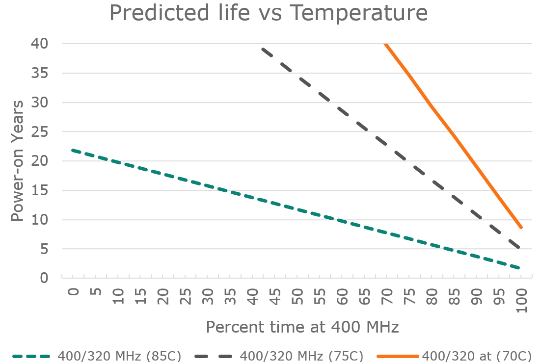
shows how junction temperature effects predicted lifetime for high performance application running 24/7 at different temperatures. If the clock duty cycle is changed from 400/320 MHz to 400/50 MHz, the predicted life under 85°C will be well above 20 years.
Summary
Very few applications require a device to run at full clock speeds continuously for the entire life of the product. Even laptop computers and smart phones run well below 50% duty cycle and below maximum junction temperature. The Infineon
PSOC™ Edge E8
devices allow the application to boost the clock to achieve burst performance, then to slow down to maximize battery life. Failure due to electro-migration only comes into play when junction temperature is over 80°C and running at the maximum clock speed. This should not be a concern for all but the most demanding applications that run 24/7.
Revision history
Document revision | Date | Description of changes |
|---|---|---|
*B | 2025-09-16 | Release to web |
Trademarks
PSOC™, formerly known as PSoC™, is a trademark of Infineon Technologies. Any references to PSoC™ in this document or others shall be deemed to refer to PSOC™.