AN236517 PCB layout guidelines for PSOC™ Edge E84 MCU
About this document
Scope and purpose
This application note provides PCB layout guidelines for a board design based on the Edge E84 MCU device. The Infineon reference schematic and layout files will be supplied (see 2 ) and form the basis of the guidelines provided.
This application note gives pointers to more highlights that are possible through placement, stack-up, routing topologies trace, etc. for
PSOC™ Edge E84
MCU devices.
Intended audience
This application note is intended for board designers.
Introduction
Packages such as fine-pitch ball grid array (FBGA), embedded wafer-level ball grid array (eWLB), and wafer-level ball grid array (WLB) are becoming increasingly popular. As they are more populated across the array with higher pin count and smaller pitch, it is important to understand how they are affected by various board layout techniques.
This application note provides a brief overview of PCB layout considerations when working with BGA packages. It outlines some of the most common problems and provides tips for avoiding them at the design stage. A key challenge of adopting fine-pitch (0.65 mm or less) BGA packages is the design of a route fanout pattern that maximizes I/O utilization while minimizing fabrication cost.
Package types
The
PSOC™ Edge
MCU product line is offered in the following packages.
Package | Description | Package dwg# |
|---|---|---|
FBGA-220 | BGA-220, 10 mm x 10 mm x 1.2 mm height with 0.65 mm pitch | PG-VFBGA-220-1 |
eWLB-235 | BGA-235, 7 mm x 7 mm x 0.685 mm height with 0.4 mm pitch | PG-WFWLB-235-1 |
WLB-154 | BGA-154, 5.281 mm x 4.281 mm x 0.505 mm height with 0.350 mm pitch | SG-XFWLB-154-1 |
See the package drawing details in the datasheet
2
for mechanical dimension details of the packages.
PCB layout routing guidelines: High-speed signals
The following guidelines provide the recommended impedance, trace width/spacing, total length limitation, and length matching requirements to achieve optimal signal integrity and timing margins.
The exact values of signal trace width and trace spacing should be determined based on the trace impedance requirement.
It is recommended to have to solid GND as reference for all signal routing layers. Reference planes should avoid any gaps or voids to minimize return current discontinuity.
Isolate the ground return path of analog signals from digital noise whenever applicable.
The power layer should only be considered as a secondary signals reference option where a solid continuous ground reference is present.
Electrical properties of the recommended signal routing are based on dielectric material with FR4 assumption.
Infineon recommends that the GND plane be used as the primary reference or return paths for all signals. Whenever a power layer is used as reference plane, it is important to ensure that the power layer is low-noise and there is proper stitching at the reference plane transitions to guarantee return path continuity (especially at high frequency).
Consider performing signal integrity simulations using Infineon-provided IBIS models to determine actual guidelines suitable for your application. The following guidelines should be used as a starting reference.
MIPI-DSI
Figure 1.
MIPI-DSI layout
Line impedance: Differential 100 Ω ± 10%
Line length difference: The line length between the differential clock and differential data should be the same length as much as possible ± 25 mil (CK/CK# to DQ ± 25 mils)
Signal line layer: The numbers of vias between differential clocks should be maintained at the same number of vias for break out and layer transition
Recommended routing: Top layer without any vias. In case of internal layer routing, same via number (the number should be as few as possible)
Return path: Place continuous ground plane under differential-signal placed GND through-hole via next to signal through-hole placed GND vias symmetrically next to differential signals
Between differential and next differential : ≥ 3S when there is no GND shield
Minimum trace width and trace spacing is based on via size defined inside the BGA area. Once the routing clears the breakout region, it is recommended to follow the general routing guidelines. It is preferable to use µvias or buried vias instead of through-hole vias to avoid neck width issues.
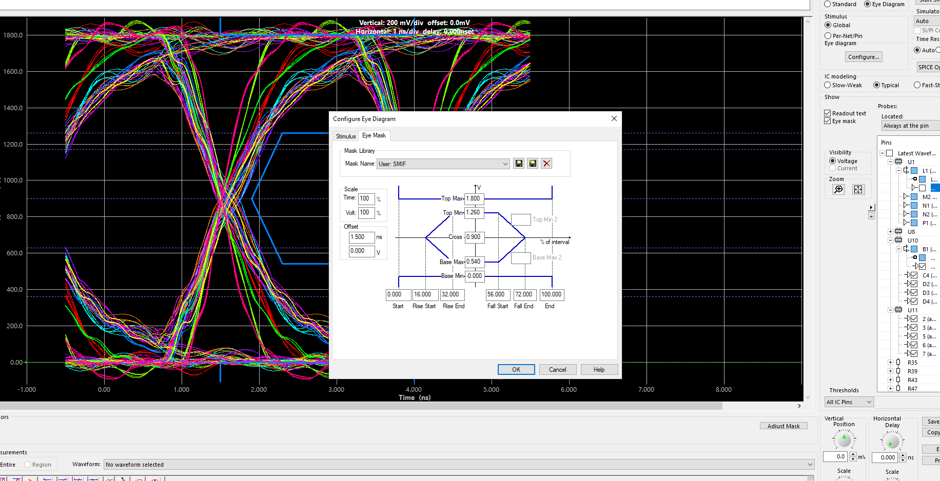
Serial memory interface (SMIF0/SMIF1)
Figure 2.
Serial memory interface (SMIF0/SMIF1)
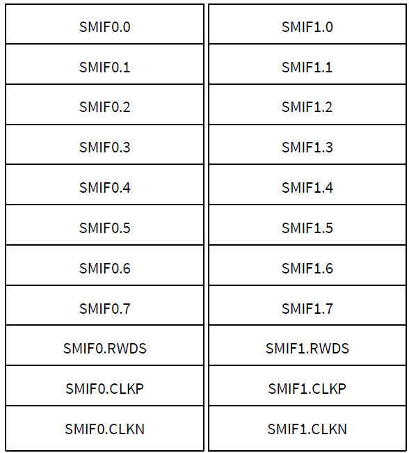
Line impedance: Differential 100 Ω ± 10%, Single ended 50 Ω ± 10%
Line length difference: The line length between differential clock should be the same length as much as possible (± 1 mils). Total line length should be as short as possible. (CK/CK# to DQ ± 500 mils)
Signal line layer: The numbers of vias between differential clocks should be maintained at the same number of vias for break out and layer transition
Recommended routing: Top layer without any vias in case of internal layer routing Same via the number (the number is as few as possible)
Return path: Place continuous ground plane under differential-signal placed GND through-hole via next to signal through-hole placed GND vias symmetrically next to differential signals
The skew is introduced into the clock system by unequal trace lengths. To minimize the board skew, keep the trace lengths equal between the data and clock.
Minimum trace width and trace spacing based on via size should be defined inside the BGA area. Once the routing clears the breakout region, it is recommended to follow the general routing guidelines.
USB 2.0
Line impedance: Differential 90 Ω ± 10%
Line length difference:
Differential pair trace length P and N should be kept same as much as possible and line length as short as possible
Return path: Place continuous ground plane under differential-placed GND through-hole next to signal through-hole placed GND vias symmetrically next to differential
The skew is introduced into the system by unequal trace lengths. To minimize the board skew, keep the trace lengths equal between P and N.
Peripherals | Impedance and tolerance | Routing | Frequency |
|---|---|---|---|
MIPI-DSI | 100 Ω +/- 10% | Differential | 1500 Mbps |
SMIF | 50 and 100 Ω +/- 10% | Differential and single-ended | 200 MHz |
USB | 90 Ω +/- 10% | Differential | 480 Mbps |
HDI vias and stack-up design
PCB designers need to figure out the number of layers required to fan out a FBGA-220. Consequently, the designer determines on which layers the critical signals are routed and the number of power and ground layers required. All the parameters described in
PCB layout routing guidelines: High-speed signals
help determine the number of layers in the stack.
HDI vias routing:
HDI type via interconnect is used for this complex board break out.
Advantages
This stack via technology results in a board that is highly routable
Minimum layers are enough to complete the breakout and routing
Disadvantages
Extra steps are required in the processing flow due to special drilling and plating of the lamination
Figure 3.
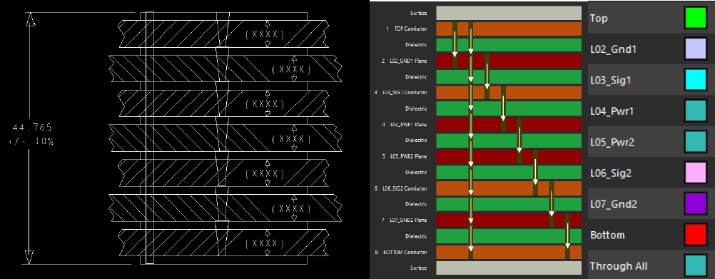
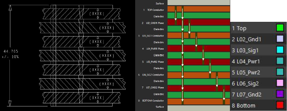
Stack-up pattern
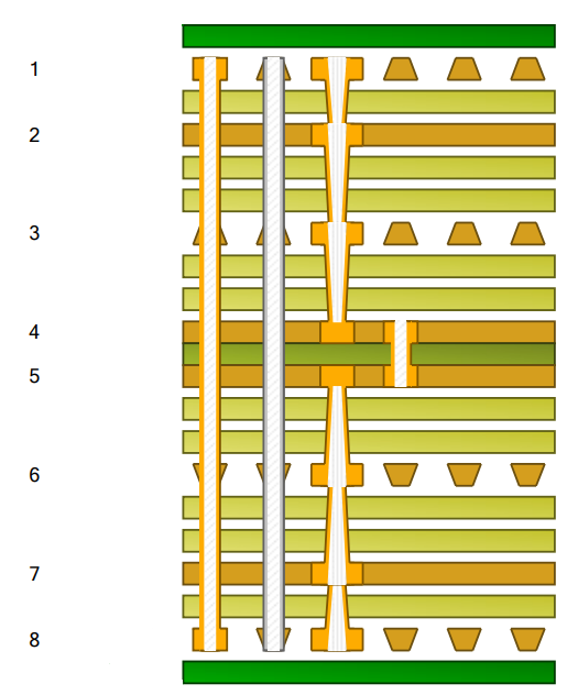
Figure 4.
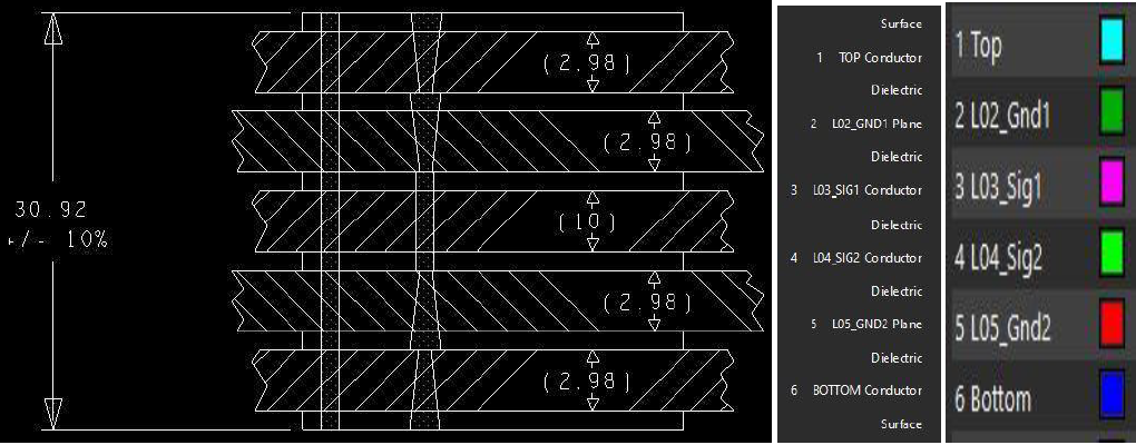
1.2 mm, 8-layer PCB stack-up
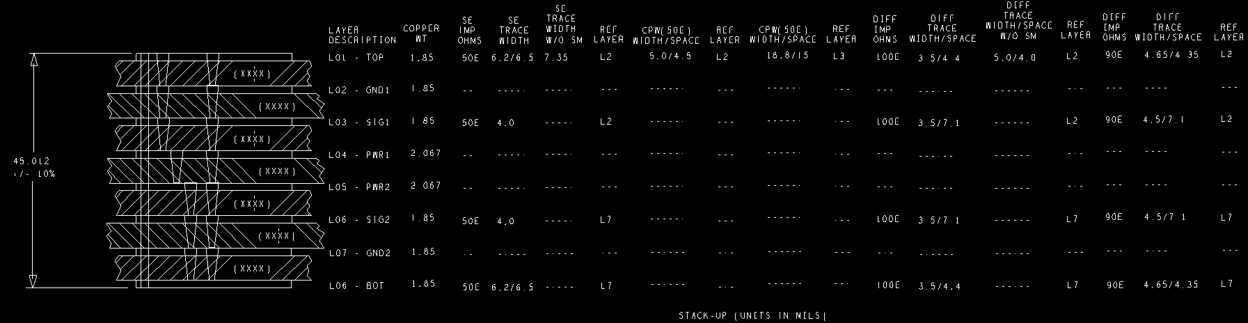
A total of eight layers are used and materials used are
FR4
or equivalent. The dielectric constant (Er) or relative permittivity (Dk) of a PCB material is generally between 4.3 and 4.8. A material's Er level depends on the frequency and will usually drop as the frequency rises.
Placement and floor planning
The floor plan links the schematic drawing and the layout. It provides a head start to the designer on component placement. A pre-placement floor plan will allow optimization of the component placement form factor and signal integrity goals. Also, the small components, like bypass capacitors and termination resistors, should be placed at an early stage. The functional blocks of circuitry like power conditioning, digital, analog, etc., should be arranged as groups to reduce signal crossing.
A floor plan gives an insight into how the signals flow between functional blocks.
For an efficient board;
Group the power conditioning together so that their signals do not have to cross through sensitive areas of circuitry
Plan your placement to keep the connection lengths as short as possible
Place the components that are part of high-speed signal paths where multiple nets connect a series of components close together
Consider the routing channels while planning the component placement to ensure there is adequate space
Consider the requirements of power and ground planes should when planning out the placement of functional blocks of circuitry
When dealing with split power planes, be cautious while placing the connected components across the split. The high-speed transmission lines should not cross the splits in power planes since it will break up the return path for those signals. Finally, avoid placing components of a different functional group during another circuit. even this will affect the return path of the circuit.
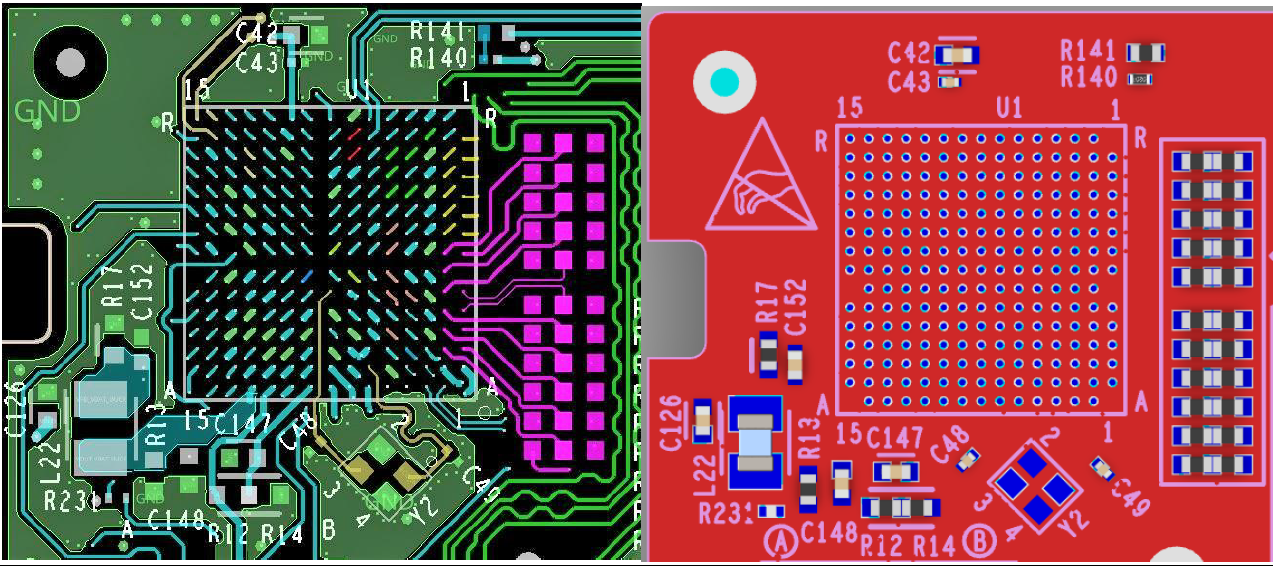
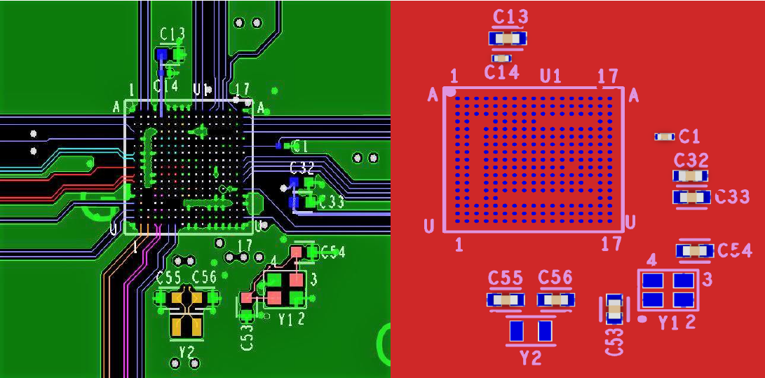
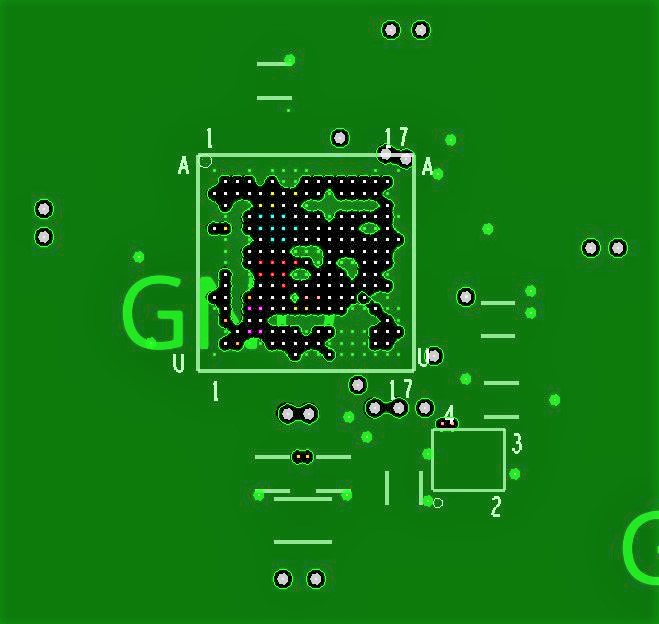
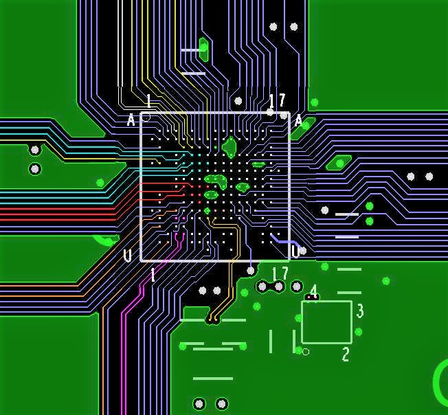
The following figures show the
PSOC™ Edge E84
MCU FBGA-220 placement and associated parts placement.
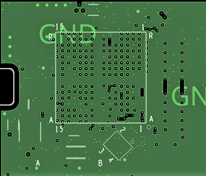
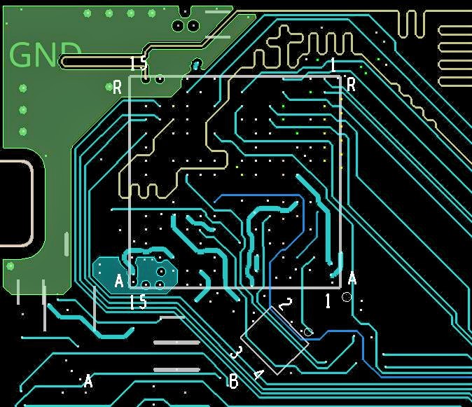
Figure 5.
PSOC™ Edge E84
MCU - Top view
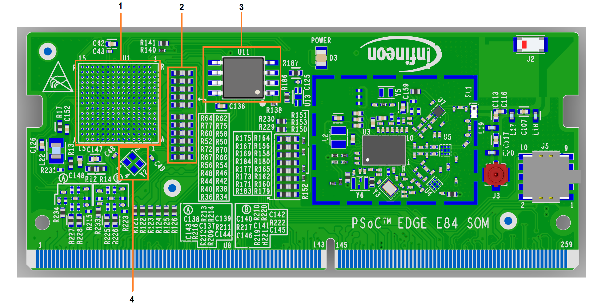
Figure 6.
PSOC™ Edge E84
MCU - Bottom view
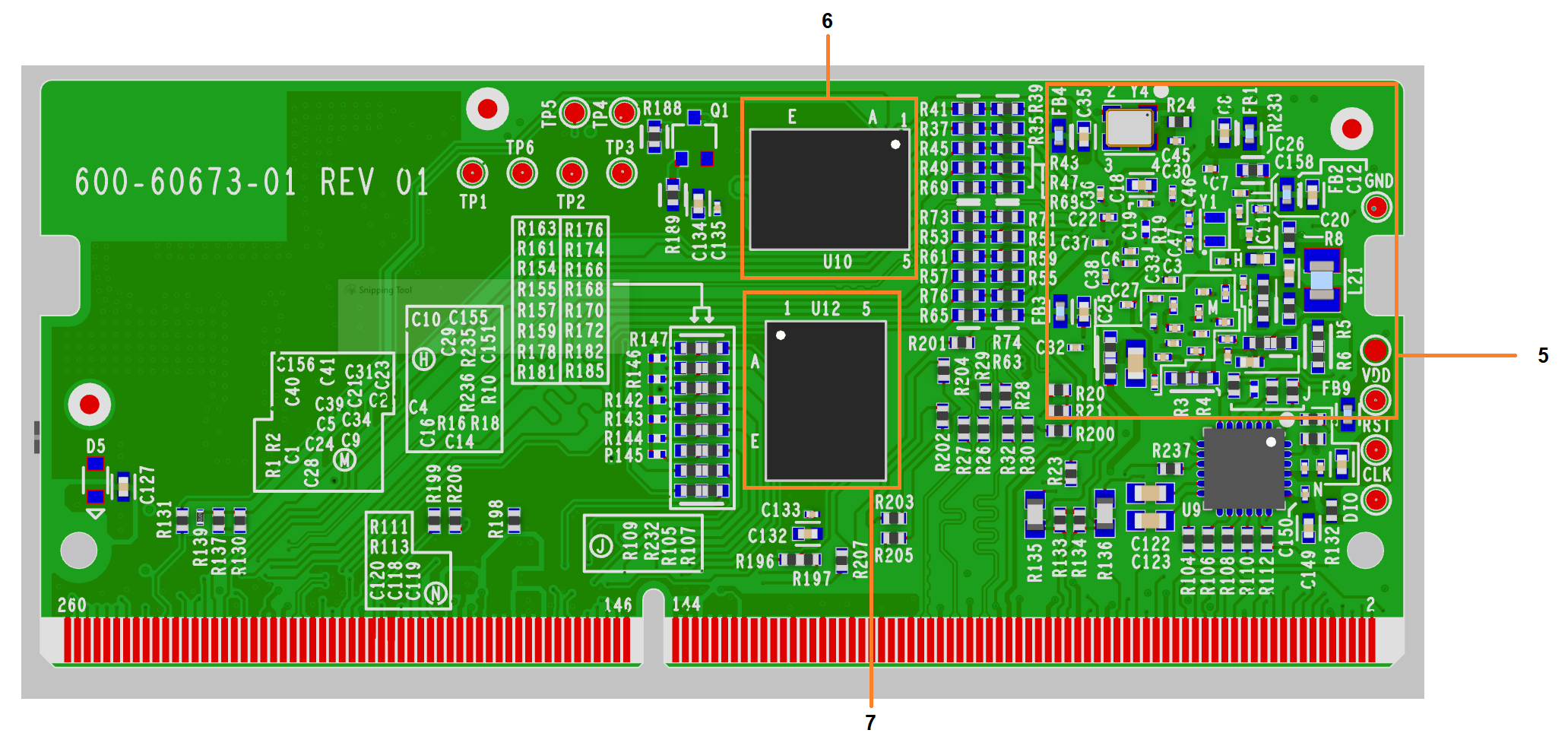
Where:
PSOC™ Edge E84
MCU (FBGA-220, U1)
Termination resistors
128-Mbit Quad-SPI NOR flash
XTAL, 17.2032 MHz, 10 ppm
PSOC™ Edge E84
MCU (FBGA-220, U1) Decoupling capacitors and associated parts
1-Gbit Octal-SPI NOR flash (U10)
128-Mbit Octal-SPI HYPERRAM™ (U12)
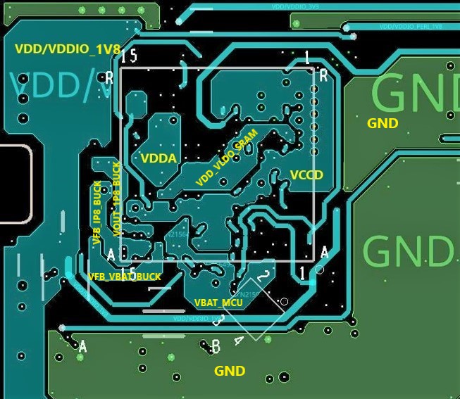
Components, bypass-, and de-coupling capacitors
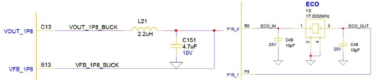
The standard decoupler for external power is a 1 µF capacitor.
Supplementary 0.1 μF capacitors should be placed as close as possible to the VSS and VDD pins of the device to reduce high-frequency power supply ripple. Generally, decouple all sensitive or noisy signals to improve the EMC performance. Decoupling can be both capacitive and inductive.
The decoupling capacitors and the inductor (buck inductor) should be placed as close as possible to the device pins with minimum trace resistance.
Figure 7.
Capacitor and inductor PCB secondary side placement
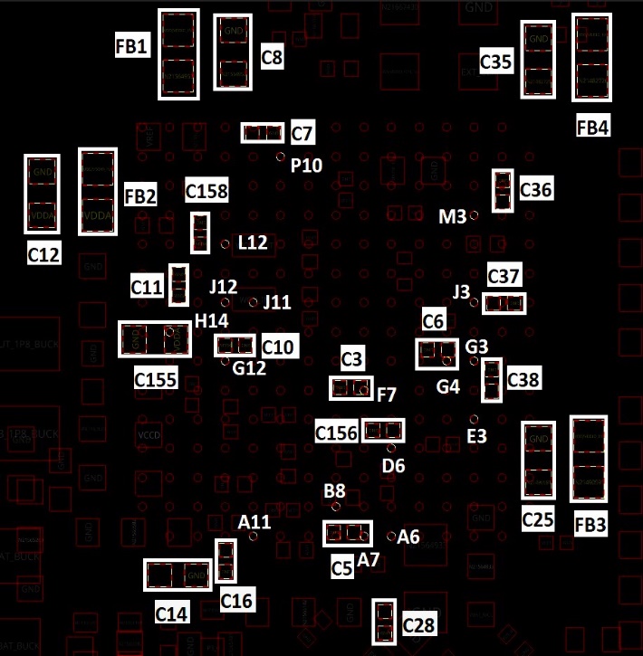
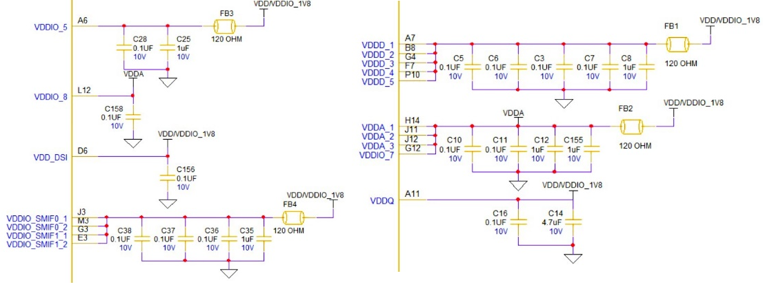
Figure 8.
Capacitor and inductor schematic sect
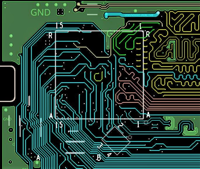
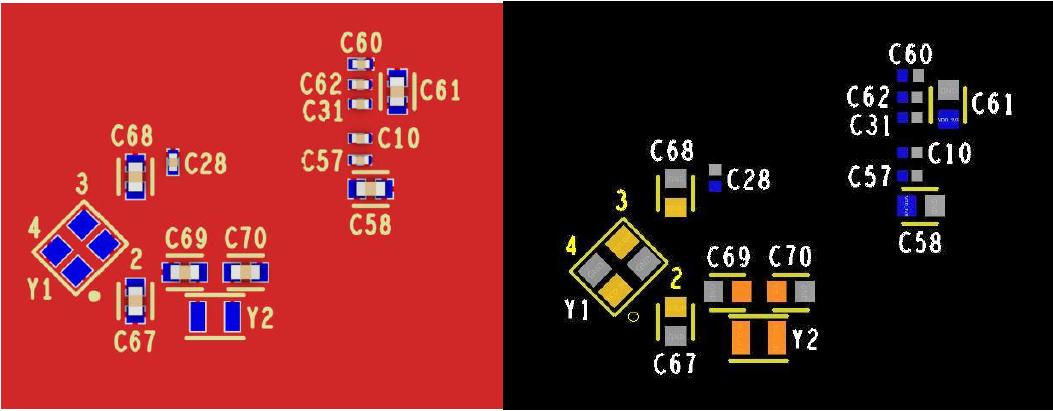
Serial interface component placements
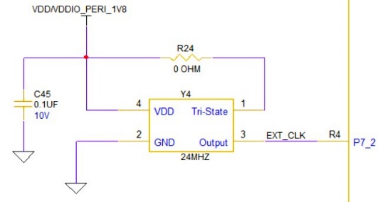
Segregate the circuits on the PCB according to their functional contribution. This helps reduce cross-coupling on the PCB. For example, separate all critical control impedance circuits, analog, CAPSENSE™ circuits. The crystal oscillator placement is critical and trace length should be as close as possible and maintain the same length ± 1 mils.
Figure 9.
Crystal placement and routing
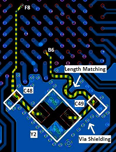
Figure 10.
Schematic section of crystal
Separate the circuits on the PCB according to their EMI contribution. This helps reduce cross-coupling on the PCB. For example, separate noisy high-current circuits, low-voltage circuits.
Figure 11.
EMI contribution-based placement
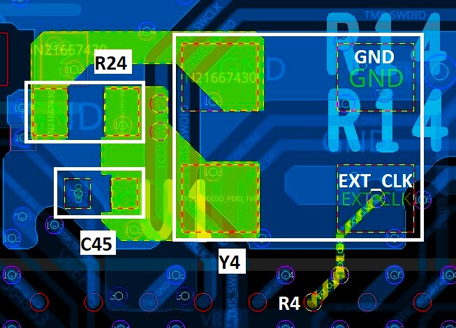
Figure 12.
EMI contribution-based placement - Schematic
Multiple power and GND distribution, vias, microvias definition
Ground and power supply
There should be a single point for gathering all ground returns. Avoid ground loops or minimize their surface area. All component-free surfaces of the PCB should be filled with additional grounding to create a shield. Especially when using high density multilayer PCBs, the power supply should be close to the ground line to minimize the area of the supply loop. Also, add sufficient copper area for high current and add sufficient vias for the path to improve current carrying capacity.
The following table provides the maximum current requirements on
PSOC™ Edge
MCU power rails.
Net name | Maximum current | Width (mils) |
|---|---|---|
VBAT_MCU | 900 mA | 25 mils |
VDDIO | 900 mA | 25 mils |
VDDA | 900 mA | 25 mils |
VDDD | 900 mA | 25 mils |
VDD_MEM_1V8 | 400 mA | 10 mils |
VDDUSB_3V3 | 300 mA | 4–5 mils |
VCCD_ANA | 60 mA | 3–4 mils |
VCCSRAM | 60 mA | 3–4 mils |
VCCRET | 20 mA | 3–4 mils |
SR Output | 400 mA | 3–4 mils |
Use power supply traces wide enough to support the required currents.
For example, a 10 mil, half-ounce copper trace can handle 500 mA (at 10°C). The width must be increased to 25 mils for 900 mA. Current carrying capacity goes up to 700 mA for 10 mils and 1.5 A for 25 mils at 30 °C for the same half-ounce copper weight.
For more information on power supply design calculations, see
PCB Design calculator
.
Microvias
Microvias handle less current than through-vias. Therefore, multiple microvias may be required in some cases.
A detailed power layout is shown in
FBGA-220 - Breakout and routing example
.
General PCB layout tips
There are many classic techniques for designing PCBs for low noise and EMC. This section describes some of these general techniques that can be used to improve the overall design of the system, EMI/EMC performance, noise handling, and so on.
Multiple layers:
Although they are more expensive, it is best to use a multi-layer PCB with separate layers dedicated to the VSS and VDD supplies. This provides good decoupling and shielding effects. Separate fills on these layers should be provided for VSS, VBAT, VDDIO, VDDA, and VDDD. In this case, you must have a good layout to support for all signal/power pins break out and taking care of all control impedance requirement, power, and ground trace. Therefore, minimum recommended layers are between six to eight
Ground and power supply:
There should be a single point for gathering all ground returns. Avoid ground loops or minimize their surface area. All component-free surfaces of the PCB should be filled with additional grounding to create a shield, especially when using six layer or eight-layer PCBs. The power supply should be close to the ground line to minimize the area of the supply loop. The supply loop can act as an antenna and can be a major emitter or receiver of EMI
Signal routing:
When designing an application, the following areas should be closely studied to improve the EMC performance:
Noisy signals, for example, signals with fast edge times
Sensitive and high-impedance signals
Signals that capture events, such as interrupts and strobe signals
To improve the EMC performance, keep the trace lengths as short as possible and isolate the traces with VSS traces. To avoid crosstalk, do not route them near to or parallel to other noisy and sensitive traces.
Controlled impedance structures in PCB and simulation results
Dos and Don'ts
Critical length:
It is exceeded when the time to propagate a conductor’s length is greater than 1/4 of the signal rise or fall time, whichever is faster. This leads to various problems.
If the total interconnect of the net is greater than its critical length, it must be managed with the constraints or different methods of managing it should be followed. Total interconnect length includes pin-package, routing, and via-used lengths.
Reference planes, termination, and impedance as they are essential for critical length nets
Maximum length constraints:
Create constraints based on edge rates to identify critical length nets in the design by classes
Placement:
Use the maximum length rule as a filter during placement to discover which nets have exceeded their critical length. Then, move the components closer to possibly prevent the nets from exceeding their critical length
Routing:
During routing, some nets may exceed their critical length due to excessive meandering. A maximum length rule would flag them
Simulation:
When working with high-speed signals, it is imperative to simulate to ensure timing, signal integrity (SI), and electromagnetic interference (EMI) problems are mitigated sufficiently to produce a layout that works as intended
Note:
Propagation delay (Tpd) of differential pairs is about 9% faster than single-ended nets in the same dielectric constant and therefore, the critical length for differential pairs is about 9% shorter.
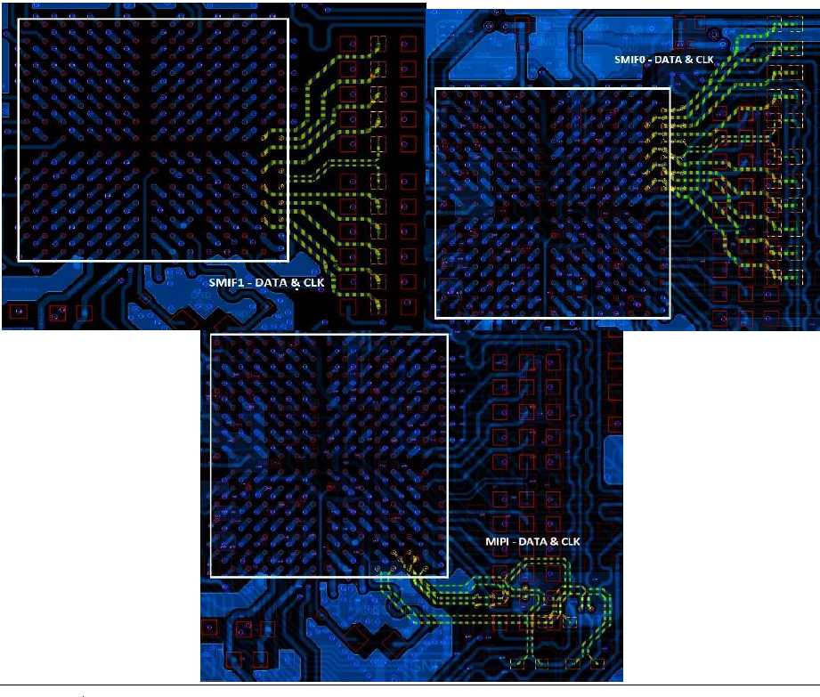
The SI report for the multi-board system for PSOC™ 6 SOM SMIF0 interface along with mating board, M.2 memory is shown in the following figures.
Single board, Octal flash, and Quad flash SMIF0 differential routing SOM board ( Figure 13 )
Single-ended clock double data rate ( Figure 14 and Figure 15 )
Figure 13. SMIF0 differential routing SOM board
Figure 14.
Output waveform at the receiver
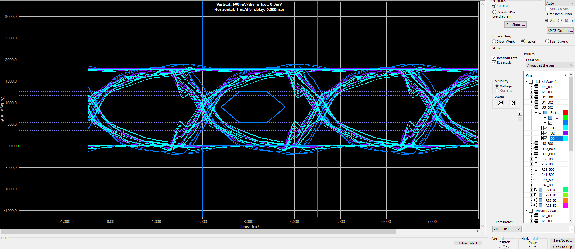
Figure 15.
Output waveform at the receiver end
Summary
All SMIF simulation is carried out with 200 MHz clock and write only operation
Even if the overall length of the trace is exceeded with respect to the datasheet, it is still within the margin for set up and hold time with fast drive mode
All the simulation is done as per the single ended clock and individual path enabled one for onboard only and another with external M.2 memory path only
All the series termination resistors are simulated with 33E for the clock and 45E for the data
Reference layers for return path of controlled impedance signals
High-speed signals must have continuous coupling to an effective copper path to establish a reference for return currents or there will be significant EMI, crosstalk, and impedance problems. The reference should be through a solid plane.
Total interconnect length includes pin-package, trace routing, and via.
Figure 16.
Reference plane for control impedance
If a critical length net is not routed on a layer adjacent to its reference plane layer, there will be significant EMI and crosstalk problems.
Get the stack-up from the manufacturer upfront or during the stating of the PCB design. Any violation on the return path and the signal will fail.
You should be clear about the edge-coupled offset strip line and edge-coupled coated microstrip patterns as this has a significant impact on the trace width for controlled impedance lines.
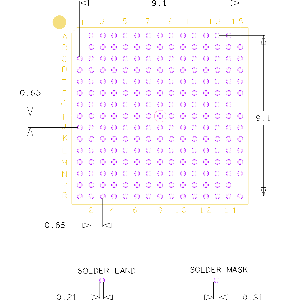
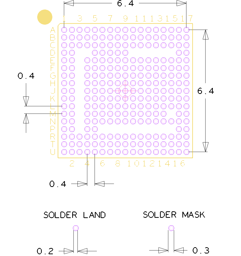
IPC class type and minimum drill and pad requirements
FBGA-220
Figure 17.
BGA 220 minimum drill and pad requirements
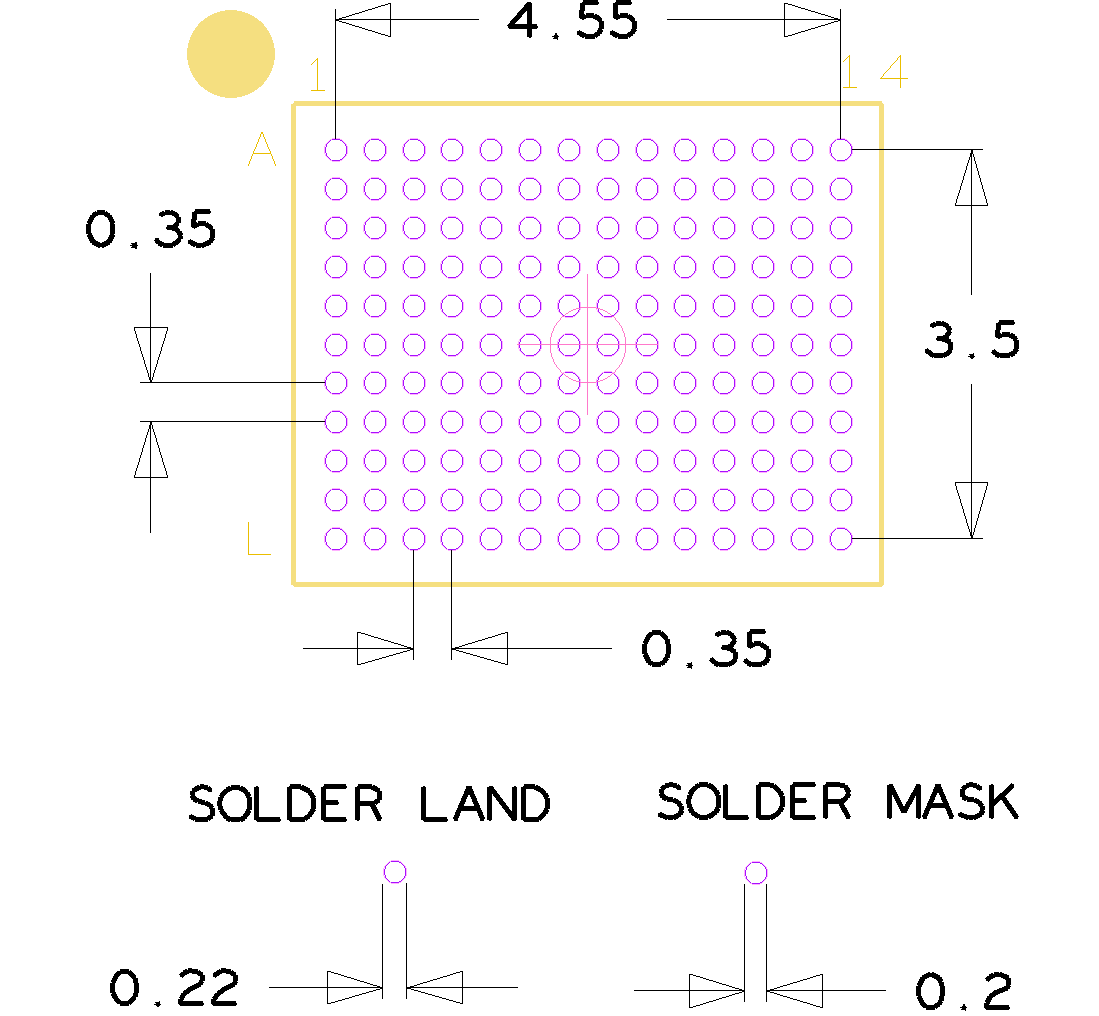
eWLB-235
Figure 18.
eWLB-235 minimum drill and pad requirements
WLB-154
Figure 19.
WLB-154 minimum drill and pad requirements
Note:
All CAD source related files, symbol, and footprint in Altium, Cadence, and Pads format link will be provided later (Weblink).
Reference board breakout and layout recommendations
Layout example summary
For mechanical dimension details see
Package types
. The following examples describe some of the routing challenges such as stackup definition, via structure, GND, and power reference plane, minimum feature requirements -minimum trace width and clearance are solved for different PSOC™ BGA package products. Examples include figures of reference layouts for all the packages. In principle, these high-level values should be considered during the initial design phase to choose a suitable manufacturer for the PSOC™ BGA package products.
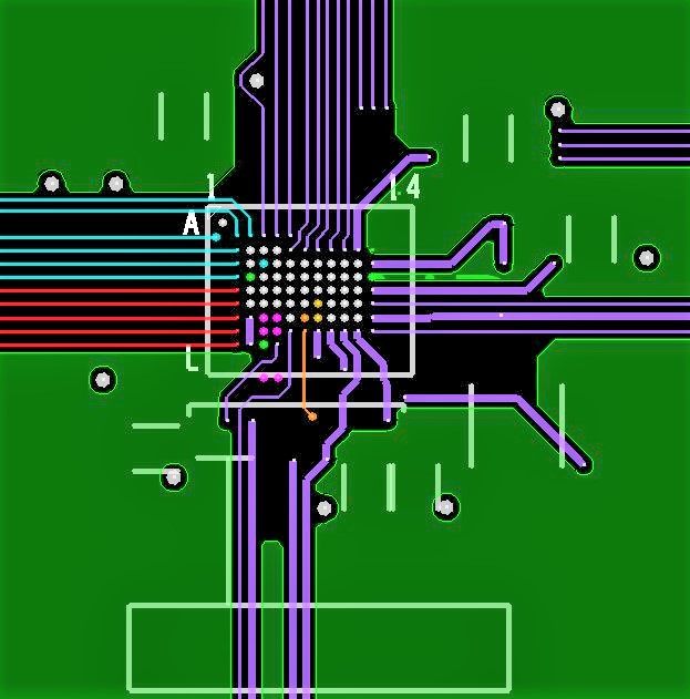
FBGA-220 - Breakout and routing example
This breakout uses a 10 mm x 10 mm size package, 0.65 mm pitch, FBGA-220 ball package in an 8-layer routing using through-via and stacked via pad of 9 mil and via drill of 4 mil technology. Flat surface at top land. This example utilizes a 3.5/3.0 mil trace width/space, other through via the pad of 16 mils, and via drill of 8 mils.
The following sections show the different layers of the of the reference board.
Figure 20.
Top placement
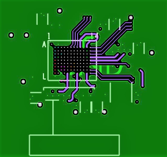
Layer 1: Component placement
Layer 1 shows how components are placed around the FBGA-220 device in the top layer. The crystal area, critical routing section, and some ground isolation areas are identified and shown in the following sections.
Figure 21.
Layer 1
The figure shows the top layer SMIF 0 and 1 signal break out routing till the termination reference board. Also, MIPI data and clock signals routing on Layer 1 shows how components are placed around the FBGA-220 device.
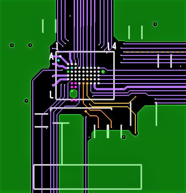
Layer 2: GND1 reference
Layer 2 (ground plane) shows the solid copper plane under the FBGA-220 device.
Figure 22.
Layer 2
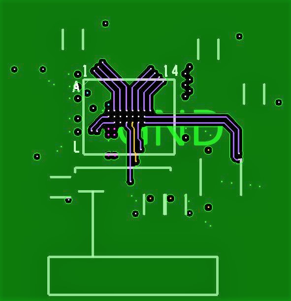
Layer 3: Signal 1
Layer 3 (signal) shows how critical controlled impedance and non-critical signals are routed around the FBGA-220 device.
Figure 23.
Layer 3

Layer 4: PWR/Signal
Layer 4 (power/signal) shows few non-critical signals that are routed around the FBGA-220 device and also a few power signals that are routed with increased trace width.
Figure 24.
Layer 4
Layer 5: PWR
Layer 5 (power) shows how all power rails are connected to support large current and low current carrying signals are routed with adequate trace width around the FBGA-220 device.
Figure 25.
Layer 5
Layer 6: Signal 2
Layer 6 (signal ) shows how critical controlled impedance and non-critical signals are routed around the FBGA-220 device.
Figure 26.
Layer 6
Layer 7: GND2 reference
Layer 7 (ground plane) shows how solid copper plane is routed under the FBGA-220 device to ensure layer 6 high speed-controlled impedance signals.
Figure 27.
Layer 7
Bottom layer
Layer 8 (bottom layer) shows how components are placed around the bottom of the FBGA-220 device. The crystal area, critical routing section, and some power, ground isolation areas are identified.
Figure 28.
Layer 8
Figure 29.
Silkscreen
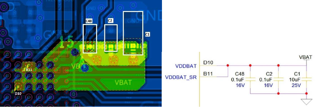
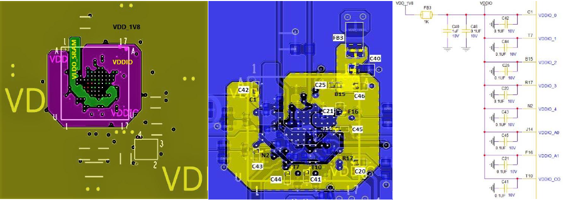
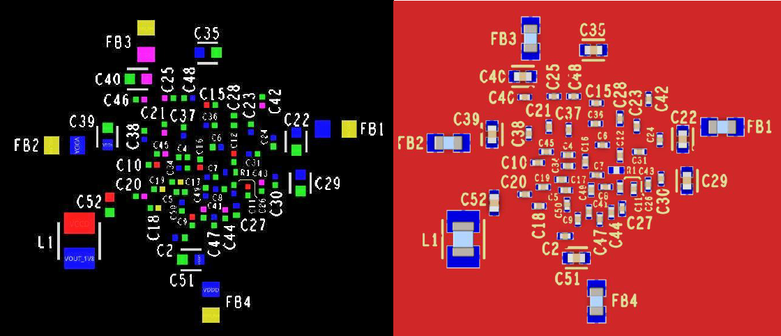
The routing and decoupling capacitor placement of key power rails such as VDD, VBAT, VDDIO, VDDIO_SMIF are shown in the following figures.
Figure 30.
VDD
Figure 31.
VDDIO
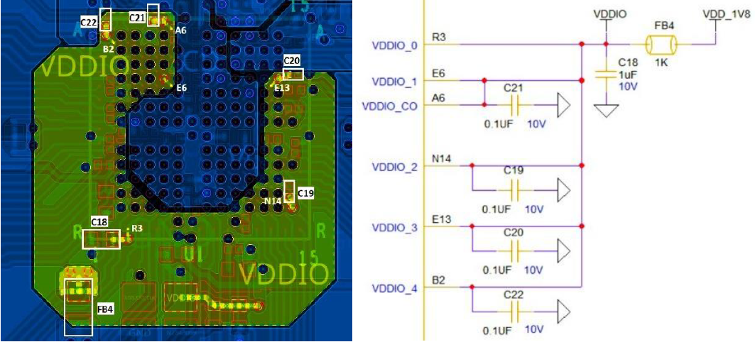
Figure 32.
VDDIO_SMIF
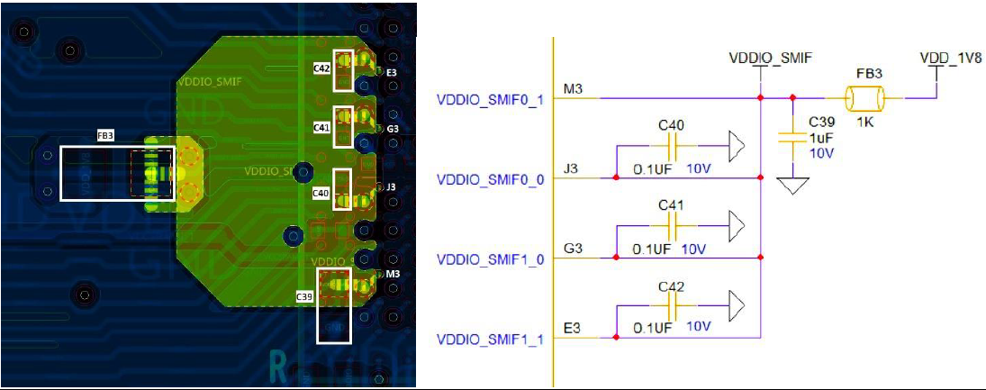
Figure 33.
VBAT
PCB stack-up and vias recommendation
This PCB stack-up construction is decided based on the component package considering signal trace density and impedance requirements for high-speed peripherals. This leads to a multilayer PCB with dedicated ground and power supply planes. Solid copper planes allow designers to keep the device ground and power connections short.
Further, the ground plane offers low inductance return paths for the high-speed signals.
Figure 34.
PCB stack-up and vias
To meet signal integrity and performance requirements, a minimum of eight-layer stack-up is recommended for implementing end-user systems. The following layer stack-ups are recommended for eight-layer boards, although other options are possible. Within a PCB it may be desirable to run traces using different methods, microstrip vs. strip line, depending on the location of the signal on the PCB. For example, it may be desirable to change layer stacking where a minimum peripheral or limited functionality is used.
PCB designers must figure out the number of layers required to fan out a FBGA-220. Consequently, the designer must determine on which layers the critical signals are routed and the number of power and ground layers required. All these parameters help determine the number of layers in the stack.
HDI vias routing:
HDI-type via interconnect is used for this complex board break out. This has the following advantages and disadvantages.
Advantages
Highly routable board
Minimum layers
Disadvantages
Extra steps in the processing flow due to special drilling and plating laminations.
eWLB-235 - Ball BGA breakout and routing example
This breakout uses a 7.5 mm x 7.5 mm size package, 0.4 mm pitch, 235-ball BGA package in an 8-layer routing using via-in-pad technology. All vias are stacked. Flat surface is at the top layer. This reference board example utilizes a 2.2/2.2 mil trace width/space, escape via pad of 9 mil and via drill of 4 mil.
Layer1: Top placement
Layer 1 (top layer) shows how components are placed around the top of the eWLB-235 device. The crystal area, critical routing section, and some ground isolation areas are identified.
Figure 35.
eWLB-235 - Layer 1
Layer 2: GND1 reference
Layer 2 (ground plane) shows the solid copper plane is routed under the eWLB-235 device.
Figure 36.
eWLB-235 - Layer 2
Layer 3: Signal 1
Layer 3 (signal) shows how critical controlled impedance and non-critical signals are routed around the eWLB-235 device.
Figure 37.
eWLB-235 - Layer 3
Layer 4: PWR
Layer 4 (power) shows how all power rails are connected to support large currents and low current power signals are routed with adequate trace width around the eWLB-235 device.
Figure 38.
eWLB-235 - Layer 4
Layer 5: PWR
Layer 5 (power) shows how all power rails are connected to support high current and low current power signals are routed with adequate trace width around the eWLB-235 device.
Figure 39.
eWLB-235 - Layer 5: High current
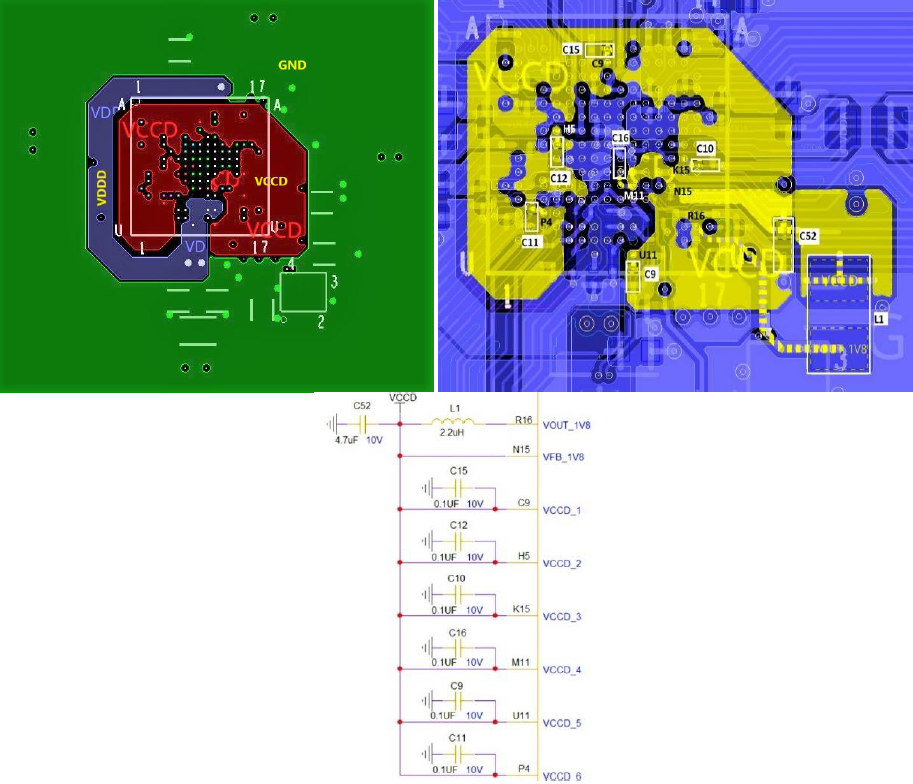
Figure 40.
eWLB-235 - Layer 5: Low current
Layer 6: Signal 2
Layer 6 (signal) shows how critical controlled impedance and non-critical signals are routed around the eWLB-235 device.
Figure 41.
eWLB-235 - Layer 6
Layer 7: GND2 reference
Layer 7 (ground plane) shows how solid copper plane under the eWLB-235 device.
Figure 42.
eWLB-235 - Layer 7
Bottom layer
Layer 8 (bottom layer) shows how components are placed around the bottom of the FBGA-220 device. The crystal area, critical routing section, and some ground isolation areas are identified.
Figure 43.
eWLB-235 – Layer 8
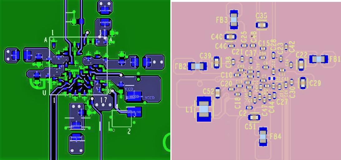
Figure 44.
VDDIO schematic section
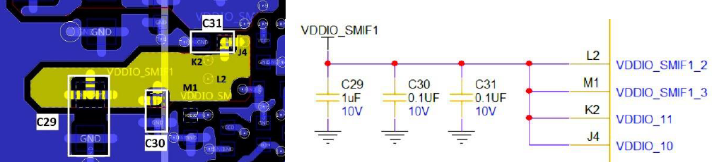
Figure 45.
VDDA schematic section
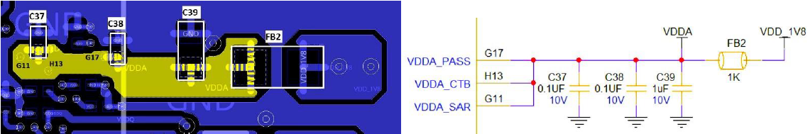
Figure 46.
eWLB-235 – Bottom layer silkscreen
PCB stack-up and vias recommendation
This PCB stake up construction decided based on the component package, considering signal trace density and impedance requirements for high-speed peripherals, it leads to multilayer PCB with dedicated ground and power supply planes. Solid copper planes allow designers to keep the device ground and power connections short.
Further, the ground plane offers low inductance return paths for the high-speed signals.
Figure 47.
PCB stack-up and vias
This PCB stake up construction is decided based on the component package, considering signal trace density and impedance requirements for high-speed peripherals, it leads to multilayer PCB with dedicated ground and power supply planes. Solid copper planes allow designers to keep the device ground and power connections short. Further, the ground plane offers low inductance return paths for the high-speed signals.
To meet signal integrity and performance requirements minimum eight-layer stack-up is recommended for implementing end-user systems. The following layer stack-ups are recommended for eight-layer boards, although other options are possible. Within a PCB it may be desirable to run traces using different methods, microstrip vs. strip line, depending on the location of the signal on the PCB. For example, it may be desirable to change layer stacking where a minimum peripheral or limited functionality is used.
WLB-154 – Ball BGA breakout and routing example
This breakout uses a 5.3 mm x 4.3 mm size package, 0.35 mm pitch, 154-ball BGA package in a 6-layer routing using via-in-pad technology. All Staked vias. Flat surface at top land. This reference board example utilizes a 2.8/2.8 mil trace width/space, escape via the pad of 9/12 mil, and via drill of 4/6 mil.
Layer 1: Top placement
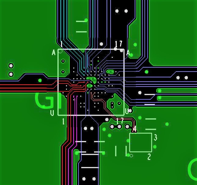
Layer 1 (top layer) shows how components are placed around the top of the WLB-154 device. Critical routing section, and some ground isolation areas are also identified.
Figure 48.
WLB-154 – Layer 1
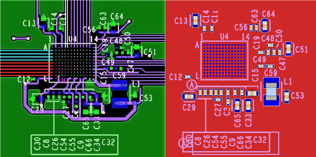
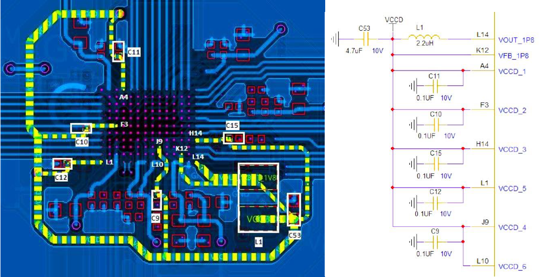
Figure 49.
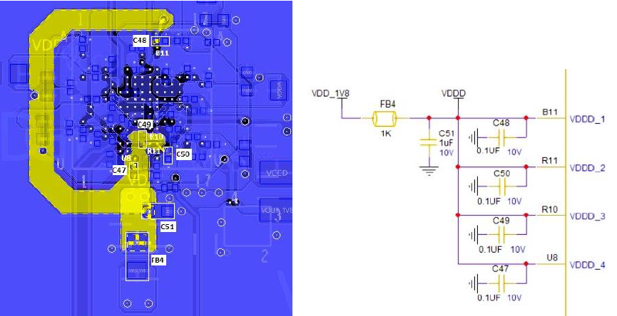
VCCD section layout and schematic
Layer 2: GND1 reference
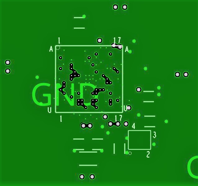
Layer 2 (ground plane) shows the solid copper plane under the WLB-154 device.
Figure 50.
WLB-154 – Layer 2
Layer 3: Signal 1
Layer 3 (signal) shows how critical controlled impedance and non-critical signals are routed around the WLB-154 device.
Figure 51.
WLB-154 – Layer 3
Layer 4: Signal 2
Layer 4 (signal) shows how all power rails are connected to support high current and low current power signals are routed with adequate trace width around the WLB-154 device.
Figure 52.
WLB-154 – Layer 4
Layer 5: GND
Layer 5 (ground plane) shows the solid GND copper plane under the WLB-154 device.
Figure 53.
WLB-154 – Layer 5
Bottom layer
Layer 6 (bottom layer) shows how components are placed around the WLB-154 device bottom. The crystal area, critical routing section, and some ground isolation areas are identified.
Figure 54.
WLB-154 – Layer 6
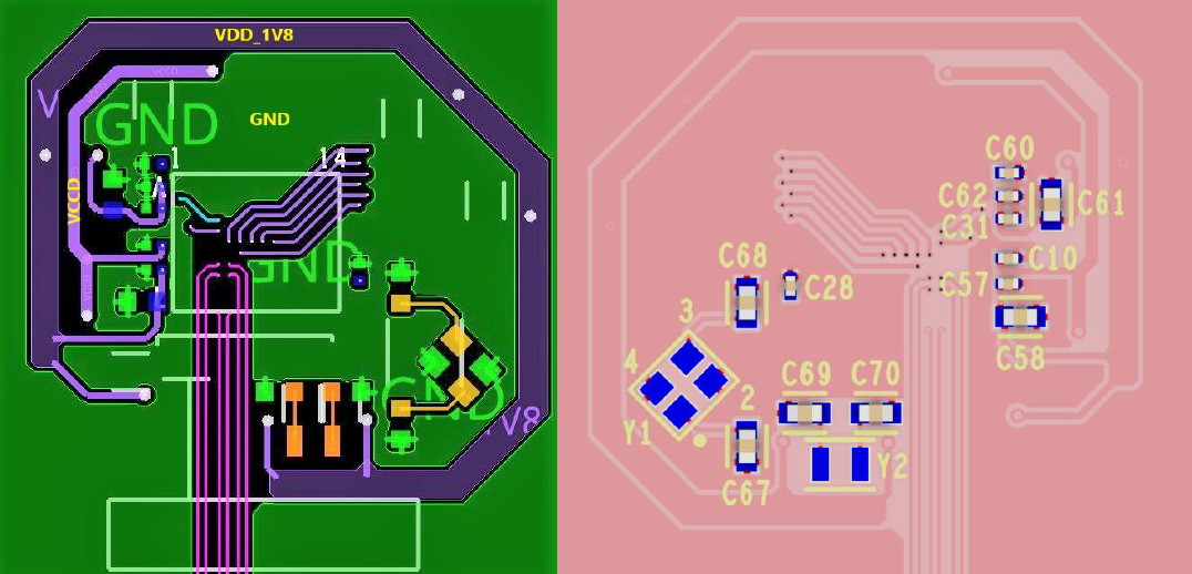
Figure 55.
Power rails
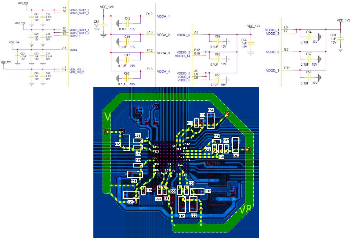
Figure 56.
WLB-154 – Bottom layer silkscreen
PCB stack-up and vias recommendation
This PCB stack-up construction is decided based on the component package, considering signal trace density and impedance requirements for high-speed peripherals. It leads to multilayer PCB with dedicated ground and power supply planes. Solid copper planes allow designers to keep the device ground and power connections short.
Further, the ground plane offers low inductance return paths for the high-speed signals.
Figure 57.
PCB stack-up and vias
To meet signal integrity and performance requirements, a minimum of six-layer stack-up is recommended for implementing end-user systems. The layer stack-ups as shown in the figure are recommended for six-layer boards, although other options are possible. Within a PCB, it may be desirable to run traces using different methods, microstrip vs. strip line, depending on the location of the signal on the PCB. For example, it may be desirable to change layer stacking where a minimum peripheral or limited functionality is used.
Layout review checklist
No | Schematic checklist | Answer (Yes/No/NA) |
|---|---|---|
1 | Are the decoupling capacitors and bulk capacitors placed close to the IC power pins? | |
2 | Is a 0.1-µF decoupling capacitor placed close to VBAT, VDDIO, VDDA, and VDDD pins? | |
3 | Are the vias placed close to the controller IC power pins? | |
4 | Are the power and switching traces routed away from the high-speed (HS) and super-speed (SS) data lines? | |
5 | Is the crystal circuitry placed close to the IC pin of the controller? | |
6 | Has a dedicated and continuous VSS plane been used? | |
7 | Are all power rails using adequate number of vias and have sufficient copper? | |
8 | Does the stack-up chosen support the controlled impedance requirements? | |
9 | Do the MIPI DSI and SMIF SS signal lines match in length? | |
10 | Do the USB SS signal lines match in length? | |
11 | Are the SMIF0,1 and MIPI SS and HS signal lines provided with a solid ground plane underneath? | |
12 | Are the MIPI DSI traces kept short? | |
13 | Do the MIPI traces have minimum bends and no 90-degree bends? | |
14 | Are the SS and HS signal trace impedance matched 50E and 100E? |
Conclusion
This application note should be used as a reference when starting a new design with an
PSOC™ Edge
MCU microcontroller. The recommendations may vary for the various packages.
References
Use the references in this section in conjunction with this document.
Note:
Infineon provides customer access to technical documentation and software through
Infineon Support Page
and Downloads and Support site (see IoT Resources).
Wafer-Level Ball Grid Array Overview and Assembly Guidelines
PSOC™ Edge
reference design. Contact your local Infineon FAE or sales representative for access to the design package including latest datasheet
EMC and System-ESD Design Guidelines for Board Layout
Design Considerations for Electrical Fast Transient (EFT) Immunity
For more information, several references are available:
The Circuit Designer's Companion, Second Edition, (EDN Series for Design Engineers), by Tim Williams
PCB Design for Real-World EMI Control (The Springer International Series in Engineering and Computer Science), by Bruce R. Archambeault and James Drewniak
Printed Circuits Handbook (McGraw Hill Handbooks), by Clyde Coombs
EMC and the Printed Circuit Board: Design, Theory, and Layout Made Simple, by Mark I. Montrose
Signal Integrity Issues and Printed Circuit Board Design, by Douglas Brooks
Rick Hartley's presentation at Altium Live, "The Extreme Importance of PC Board Stack Up" delves into creating the best stack-ups for critical length nets
Dr. Bruce Archambeault's book, "PCB Design for Real-World EMI Control," is highly recommended by Rick Hartley for identifying and solving EMI problems
Revision history
Document revision | Date | Description of changes |
|---|---|---|
*B | 2025-09-19 | Release to web |
Trademarks
PSOC™, formerly known as PSoC™, is a trademark of Infineon Technologies. Any references to PSoC™ in this document or others shall be deemed to refer to PSOC™.