AN241320 PSOC™ Edge MCU: Tamper protection and detection mechanisms
About this document
Scope and purpose
This application note provides a comprehensive overview of the security features to prevent and detect tampering using PSOC™ MCUs.
It provides fundamental concepts related to tampering and their significance in the design of modern secure embedded systems. The document then delves into the internal mechanisms that help provide tamper protection for PSOC™ MCUs, including the lock-step Secure Enclave (SE) available on PSOC™ Edge MCUs.
Furthermore, the document provides detailed descriptions of both software and hardware solutions for implementing passive and active external tamper detection using PSOC™ MCUs, enabling developers to effectively integrate robust security measures into their designs, ensuring the integrity and reliability of their embedded systems.
Note:
Note that code examples referenced in this document may not be available in ModusToolbox™ at the time of reading. The examples will be released in an upcoming BSP release.
Intended audience
This application note is intended for hardware and software developers, engineers, and system architects who are involved in the design and development of embedded systems using PSOC™ MCUs. It is also suitable for anyone seeking a better understanding of tamper protection and detection mechanisms, and their impact on embedded applications.
Introduction
Tamper of a secured device refers to the intentional modification of a system to expose items, such as cryptographic information, proprietary software, or application secrets. Modifications of a system can also allow the device to be accessed or operated by unauthorized users. When developing a secured system, consider implementing tamper protection, detection, and response mechanisms early in the design phase to ensure a robust, yet power efficient solution.
Tamper protection
Tamper protection is a set of security mechanisms designed to prevent or detect any unauthorized attempts to access, modify, or manipulate a device, system, or data. These measures can include physical, software-based, or firmware-based solutions that ensure the integrity and authenticity of the device or system. Tamper protection can be applied to various types of devices, including microcontrollers, secure elements, and other embedded systems.
Tamper mechanisms can be broadly classified into four categories, each serving a unique purpose in preventing and responding to unauthorized access or manipulation.
Tamper resistance:
The system's ability to withstand attempts at unauthorized access. This is typically achieved through the use of robust physical barriers, such as reinforced enclosures, secure locking mechanisms, encapsulation, or protective coatings
Tamper detection:
Involves identifying potential security breaches or anomalies that may indicate a tampering event. This is often accomplished through the use of sensors or switches that monitor the system's integrity
Tamper response:
Once a tampering event is detected, the system's tamper response mechanism is triggered. This can involve a range of actions, including the deletion of sensitive information, activation of a safe mode, display of a warning message, or in extreme cases, the complete destruction of the application, system, or device
Tamper evidence:
The system's ability to record and preserve evidence of the tampering event. This can take the form of physical evidence, such as a broken seal, or digital records, including logs and reports of the incident
Device-level vs. system-level tamper protection
Tamper protection levels can vary significantly across different embedded systems, and as such, tamper mechanisms must be designed to accommodate these varying requirements. For instance, some systems may only necessitate evidence of tampering, which can be achieved through the use of a seal, often for warranty purposes. In contrast, other systems may demand more stringent measures, such as completely erasing the device, even if it means rendering the application inoperable.
Some tamper mechanisms, particularly those related to tamper resistance and evidence, are typically implemented at the system level. These mechanisms can incorporate mechanical components that operate independently of the MCU.
On the other hand, tamper detection and response mechanisms often rely on the MCU's intervention. This is because MCUs are typically the central component of an embedded system and because they often contain sensitive information, including code, data, and cryptographic keys. For this reason, the MCU's involvement is necessary for implementing sensing mechanisms and responding to potential tampering events, as well as erasing sensitive data or reporting events.
This application note focuses on tamper detection and response mechanisms relevant to PSOC™ MCUs, and while many of the solutions and concepts are MCU-agnostic, this document focuses on the implementation using PSOC™ Edge MCU. The
Tamper protection mechanisms
section discusses different mechanisms, which are either inherent to the device or can be optionally implemented to improve the security of the application; while the
External tamper detection mechanisms
section discusses mechanisms for detection of external tampering.
Tamper protection mechanisms
Tamper protection works by implementing various security measures to prevent or detect unauthorized access or modifications to a device or system. These measures can include:
Intrusion detection systems:
Detecting and alerting on potential security threats
Encryption mechanisms:
Encrypting data to prevent unauthorized access
Secure boot and authentication mechanisms:
Ensuring that only authorized firmware is loaded onto a device
Intrusion detection systems
Temperature monitoring
Temperature tampering involves manipulating a system's operating temperature to compromise its security or functionality. This can be done by exposing the system to extreme temperatures, such as high heat or cold, or by using a thermal interface material to alter the system's thermal characteristics. Temperature tampering can cause a range of problems, including data corruption, system crashes, and even physical damage to the system's components.
PSOC™ MCUs can leverage internal or external temperature sensors to monitor temperature periodically using the integrated ADC or comparators, and trigger warnings or events if an intrusion is detected. The
Autonomous Analog
module included in some PSOC™ MCUs can perform ADC conversions autonomously in Deep Sleep mode and without CPU intervention, allowing to reduce power consumption significantly.
PSOC™ Edge MCUs include an autonomous analog module and an internal temperature sensor, which can be used by the application to read temperature at any time; as well as a secure non-modifiable boot code, which inherently reads the temperature sensor to validate that the system is working at an expected temperature range when performing security-critical operations, such as true random generator (TRNG).
Voltage monitoring
Voltage tampering refers to the intentional manipulation of a system's power supply voltage to compromise its security or functionality. This can be done by applying an abnormal voltage level, such as a voltage spike or a voltage drop, to the system's power input. Voltage tampering can cause a range of problems, including data corruption, system crashes, and even physical damage to the system's components.
PSOC™ MCUs can leverage integrated voltage detection peripherals, such as the low-voltage detect (LVD) or overvoltage detect (OVD) circuits, which monitor supply rails and can generate an interrupt or a fault when supplies exceed the expected voltage range; or, they can leverage internal ADCs, comparators, and bandgap voltage references to perform customized voltage monitors in the application. The autonomous analog module can also be used to perform autonomous conversions without CPU intervention in low power mode.
In addition to having LVD, OVD, and an autonomous analog module, PSOC™ Edge MCUs feature an anti-tamper voltage glitch sensor, which is enabled by the boot firmware when performing critical checks, such as firmware verification and debug policy configuration.
Secure Enclave using lockstep
In addition to having two CPUs for user application, PSOC™ Edge MCUs feature an isolated internal Secure Enclave (SE) containing two Arm® Cortex®-M0+ processors operating in lockstep, and providing runtime services for Arm® Platform Security Architecture (PSA) compliant cryptography, key management, and attestation services; available on EPC4 derivatives only.
Lockstep is a mechanism that involves running processes in parallel, with each core executing the same instructions and accessing the same data. The outputs of each core are then compared to ensure that they match. If the outputs do not match, it indicates that one of the copies has been compromised or is operating incorrectly. In this way, the Secure Enclave inherently provides a high level of protection against fault injection and semi-invasive attacks.
Additionally, the Secure Enclave provides internal secure storage, which is physically separated from the overall nonvolatile memory (NVM) and uses a dedicated access port with unique tags, and has multiple layers of protection that only the Secure Enclave can access. These mechanisms protect the Secure Enclave storage from any forms of observations.
External tamper detection
PSOC™ MCUs can leverage many different hardware and software mechanisms to detect system tampering. These mechanisms are discussed in more detail in the
External tamper detection mechanisms
section.
Encryption mechanisms
Cryptographic accelerators
Cryptographic accelerators are specialized hardware components designed to accelerate operations, such as encryption, decryption, and digital signatures. These accelerators can significantly improve the security of a system by providing a secure and efficient way to perform cryptographic operations.
PSOC™ MCUs include different hardware accelerators, which can be used to perform symmetric and asymmetric encryption and decryption, hash generation, cyclic redundancy checks (CRCs), and, random number generation.
Secure Enclave supporting cryptographic and key management services using SE_RT
PSOC™ Edge MCU is beyond regular MCUs and includes a dual cryptographic accelerator, which is only accessible by software running on the Secure Enclave and provides services protected against side-channel attacks (SCA) and differential power analysis (DPA). This secure functionality is accessible by the application through Secure Enclave runtime (SE_RT) services and provide access to PSA compliant cryptographic services, key management, attestation, and secure storage services.
shows the security architecture of PSOC™ Edge and how the SE_RT services are accessed by the application:
Figure 1.
Security architecture diagram for PSOC™ Edge MCU
SE_RT services are only available on EPC4 devices. This application note explains how to leverage them to store and delete keys in the
Erasing keys using SE RT services
section.
Encrypted memory
Using internal memory can often offer higher protection against attacks compared to external memories; however, internal memories resources are usually more limited, requiring developers to use external memories to store large amounts of code or data and creating a potential target for attacks.
External memories can be attacked by eavesdropping or modifying data; however, such attacks can be protected by encrypting memory contents.
PSOC™ Edge MCUs support on-the-fly encryption and decryption of external memories using the integrated Serial Memory Interface (SMIF). The device can either read and write encrypted data and code from external memories using APIs in Memory-Mapped I/O (MMIO) mode, or it can execute code directly in Execute in Place (XIP) mode.
Note that external storage is not DPA protected. It is recommended to use the Secure Enclave internal storage to store application secrets; or use the Secure Enclave cryptography to process externally stored secrets.
Secure boot and authentication mechanisms
Secure boot and chain of trust
Secure boot mechanisms involve a combination of hardware and software components that work together to verify the authenticity and integrity of the system's firmware or software.
While secure boot mechanisms can be implemented in software for practically any microcontroller, PSOC™ Edge MCUs offer a highly secure solution by leveraging the Secure Enclave and ROM code, as shown in
Figure 2
.
Figure 2.
Chain of trust using PSOC™ Edge MCU
The basis of the chain of trust relies on the root-of-trust (RoT), which is memory that cannot be changed. In PSOC™ Edge, the RoT starts with the Secure Enclave booting from the internal ROM, which then verifies the second part of the boot code in secured RRAM. The Secure Enclave then verifies the first CM33 code area in RRAM which contains the extended boot, which subsequently checks the OEM policy file and validates the user application when enabled.
This mechanism ensures that the boot code is immutable and that the chain of trust is extended all the way to the application.
When secure boot is enabled, any unexpected code alterations will be detected by this mechanism, preventing execution of invalid or non-authenticated code.
For more information about these secure boot mechanisms and how to use them, see the
AN237849 – Getting started with PSOC™ Edge Security
application note.
Edge Protect Bootloader
While the integrated ROM boot and extended boot included in PSOC™ Edge can be used to validate the first secure CM33 application; it is also possible to use Edge Protect Bootloader to extend the chain of trust to all the application projects.
Edge Protect Bootloader consists of a port of the open-source MCUboot and it can be optionally enabled on PSOC™ Edge devices. ModusToolbox™ includes examples explaining how to add support to any application.
For more information about Edge Protect Bootloader and how to use it, see the
AN237849 – Getting started with PSOC™ Edge Security
application note.
Authenticated debug
The device debug interface (for example, JTAG or SWD) is a commonly attacked communication interface, which can be used to gain access to the device, including memory, CPU, and security assets.
Most microcontrollers provide means to disable debug interfaces using hardware or software fuses, while more sophisticated solutions can support debug authentication.
PSOC™ Edge goes a step beyond by implementing multiple device lifecycle stages (LCS). The following stages are relevant to product developers:
Development LCS:
This is the default state of the device, allowing the device to be provisioned and programmed as many times as needed to develop the final application. During development, the OEM may take ownership of the device, allowing to replace the default policy file with a custom one. A customized policy file can be used to enable and disable the debug interface, or to allow debug access only under certain conditions such as presenting a debug certificate. It is not recommended to ship the final product in this lifecycle stage
Production LCS:
This state locks down the ownership of the device, meaning that the key used to authenticate the firmware can no longer be changed from what was programmed into the device. The debug ports, including SYS_AP, can all be disabled or left enabled with or without authentication as per user requirement
Return merchandise authorization (RMA):
This lifecycle should be used when customers require Infineon to perform failure analysis. In the RMA LCS, the device can no longer be provisioned. All device secrets are wiped out from the device. After the device is moved into the RMA mode, when it boots, it does not attempt to execute any code in the user flash; instead, it waits for the OpenRMA token through the debug port, signed by Infineon to enable further internal debug and analysis of the device by Infineon. Note that once the device is in RMA lifecycle stage, it can no longer be used in an application
Software running on the Secure Enclave is responsible for parsing the debug policies and enforcing them on every boot, making it part of the root-of-trust.
For more information about authenticated debug and lifecycle stages, see the AN239757 – Authenticated debug for PSOC™ Edge application note.
External tamper detection mechanisms
External tamper detection involves using device pins to detect when the system encounters unauthorized access or tampering. The microcontroller continuously compares a received signal with a known level and it triggers a tamper event when a mismatch is detected. Different mechanisms can be used to detect external tampering, but a common one is using mechanical switches or a tamper mesh, in the form of a network of conductive paths, which typically open when the system is tampered with.
Passive and active detection
The distinction between passive and active implementations lies in the nature of the received signal. If the signal remains static or unchanging, the implementation is considered passive. On the other hand, if the signal is dynamic, constantly switching or fluctuating, the implementation is classified as active.
shows the basic concepts of typical external tamper implementations:
Figure 3.
Basic concepts of external tamper detection mechanisms
Figure 3 A) shows the basic concept of a passive tamper implementation using a normally closed (NC) switch. The TAMPER_OUT signal can be used to drive a LOW signal, which is detected by the TAMPER_IN line when idle. When the circuit opens due to a tamper event, a pull-up resistor drives the line high, causing a trigger, which is detected by the microcontroller GPIO. Note that a circuit from VCC to ground forms through the resistor, causing an idle current . Because of this reason, it is typically recommended to use external resistors with high value to reduce power consumption. Additionally, TAMPER_OUT can be used to drive a LOW signal when tamper detection is enabled, but it can also be left open to disable the circuitry; or alternatively, the switch can be connected directly to ground to enable the circuit all the time. Note that the Figure 3 shows an implementation when the idle signal is LOW, but the same concept applies with the opposite polarity.
B) uses a normally open (NO) switch. The implementation is similar, but there is no path from VCC to ground, so the idle current is minimal and only due to GPIO leakage when the circuit is idle. Similar to the previous implementation, TAMPER_OUT can be used to disable the circuitry, or the switch can be connected to the ground directly if needed; and the same concept applies with the opposite polarity by using a pull-down resistor on TAMPER_IN, and driving a logic high through TAMPER_OUT.
C) shows a basic concept of an active tamper mechanism. As observed, a signal is actively driven with a pattern using TAMPER_OUT, and the same signal is received on TAMPER_IN when the circuit is idle; however, the circuit breaks when the switch is open and a mismatch is detected. Note that this implementation requires microcontroller resources both to drive the output pattern, and to actively compare it with the incoming signal. Since the signal is driven actively with push-pull I/Os, a pull resistor can be used, but it is optional.
PSOC™ devices can implement passive and active detection circuits in different ways, but this application note will show a detailed implementation of one active and two passive mechanisms, and it will discuss other options in the
Alternative tamper detection implementations
section.
Application flow diagram
shows the basic flow of an application implementing tamper detection using PSOC™ Edge MCUs:
Figure 4.
Flow diagram for tamper detection application using Hibernate or Deep Sleep-OFF
Execution starts after reset from the Secure Enclave, which validates and executes extended boot. If secure boot is enabled, extended boot validates and executes the first user application CM33_S, which is executed in a secure environment using the Cortex® M33 CPU. If secure boot is disabled, extended boot simply boots the CM33_S application without validating it.
The CM33_S application takes care of initializing the tamper peripherals, circuitry, and interrupts; handling the interrupt and wake up events when a tamper event is detected; implementing the tamper response mechanism. Note that
Figure 4
shows the implementation of a tamper mechanism using Hibernate or Deep Sleep-OFF modes, where the device goes through a cold boot process after waking-up. The tradeoffs between different low power modes are explained in the
Low-power modes for tamper detection applications
section. The implementation of the tamper detection mechanisms are explained in more detail in the
Passive tamper detection
and
Active tamper detection
sections, while tamper response mechanisms are explained in the
Tamper response mechanisms
section.
After the tamper functionality is initialized, the CM33_S application continues with the initialization of the rest of the system, and then launches the non-secure M33 application (CM33_NS), which will subsequently launch the M55 application (CM55). While it is possible to implement tamper detection on CM33_NS or CM55, it is usually preferred and recommended doing it in the secure environment of CM33_S.
Note that when secure boot is enabled in extended boot, it only validates the CM33_NS application; however, it is possible to use other solutions, such as Edge Protect Bootloader to validate all other projects and data.
Low-power modes for tamper detection applications
For numerous applications, it is crucial to strike a balance between low power consumption and the ability to continuously and securely detect tamper events. PSOC™ MCUs address this need by offering a range of low-power modes, providing users with high flexibility in terms of power consumption, device functionality, and wakeup times.
The following table summarizes the system power modes supported on the PSOC™ Edge MCU:
Sleep | System Deep Sleep | System Deep Sleep-OFF | System Hibernate | |
|---|---|---|---|---|
Wakeup source | Any interrupt | Deep Sleep peripherals | Deep Sleep peripherals | RTC/Hibernate peripherals |
Wakeup action | Resume | Resume | Reset/cold boot | Reset/cold boot |
Wakeup time | 1 CPU cycle | < 20 μs | Deep Sleep + cold boot (~25 ms to >200 ms) | POR (~540 μs) + cold boot (~25 ms to >200 ms) |
SRAM retention | On/select off | Off/select retention | Off | Off |
Sleep:
This mode provides the most functionality since only the CPU halts execution while the rest of the system is functional and any interrupt can wake up the device with minimum latency; however, it consumes the most power.
System Deep Sleep:
It is achieved when both CPUs enter Deep Sleep and it results in a significantly reduced power consumption, at a cost of limited device functionality and longer wake-up times. In this mode, the system clocks are limited, which restricts the peripherals that can wake up the device; however, a range of common peripherals used in low-power modes are still supported, including I2S, SPI, the autonomous analog module, Smart I/O, RTC, among others. This ensures that the device can still respond to critical events and maintain high functionality, even in a low-power state. Additionally, SRAM can be selectively retained, allowing developers to carefully balance power consumption and performance. System Deep Sleep mode offers a high degree of flexibility, allowing developers to fine-tune power consumption to meet the specific needs of their application.
System Deep Sleep-OFF:
It is a sub-mode of system Deep Sleep, which reduces power consumption even more, but it completely turns off SRAM and other internal circuitry resulting in longer wake-up time. Deep Sleep-OFF can use the same peripherals as Deep Sleep and it can retain volatile application data using backup registers (BREG); however, the device goes through a cold boot process when waking up, as shown in
Figure 4
. The cold boot wakeup time depends on the system configuration, but it is around 25 ms when secure boot is disabled, or around 200 ms plus a time depending on image size when secure boot is enabled. For actual wakeup times, see the corresponding device datasheet.
System Hibernate:
This mode has similar wakeup times as Deep Sleep-OFF, since it goes through the cold boot process, and it also does not retain SRAM; however, it offers the lowest power consumption with a tradeoff of more limited wakeup sources. PSOC™ Edge MCU enables wakeup from Hibernate mode using selected GPIO pins, real time clock (RTC), watchdog timer (WDT), and the low-power comparator (LPCOMP), and it also allows for retention of some volatile data using backup registers.
This application note shows solutions using system Hibernate and system Deep Sleep-OFF as they offer the lowest power consumption; however, other modes can be used instead if more functionality is desired in low-power mode, or when requiring faster wakeup times.
Passive tamper detection
Passive tamper detection involves monitoring a fixed signal and triggering an event when any changes are detected. The signal is typically a digital HIGH or LOW, but it can also be an analog voltage level. This method can be implemented on normally closed (NC) or normally open (NO) tamper switches and requires minimal hardware resources.
Passive tamper implementation using GPIOs
A basic external passive tamper detection solution can be implemented using GPIOs. In this approach, the tamper circuit stays at a known fixed level when idle, and toggles with a tampering event.
As previously shown in
Figure 3
, this approach can be implemented with NC and NO switches; however, the solution described in this document uses a simple NC switch, which can be easily implemented with traces or wires which open the circuit when the system is tampered with.
Hardware and device implementation
The schematics of the solution are shown in
Figure 5
:
Figure 5.
Schematics for single tamper line solution using GPIOs
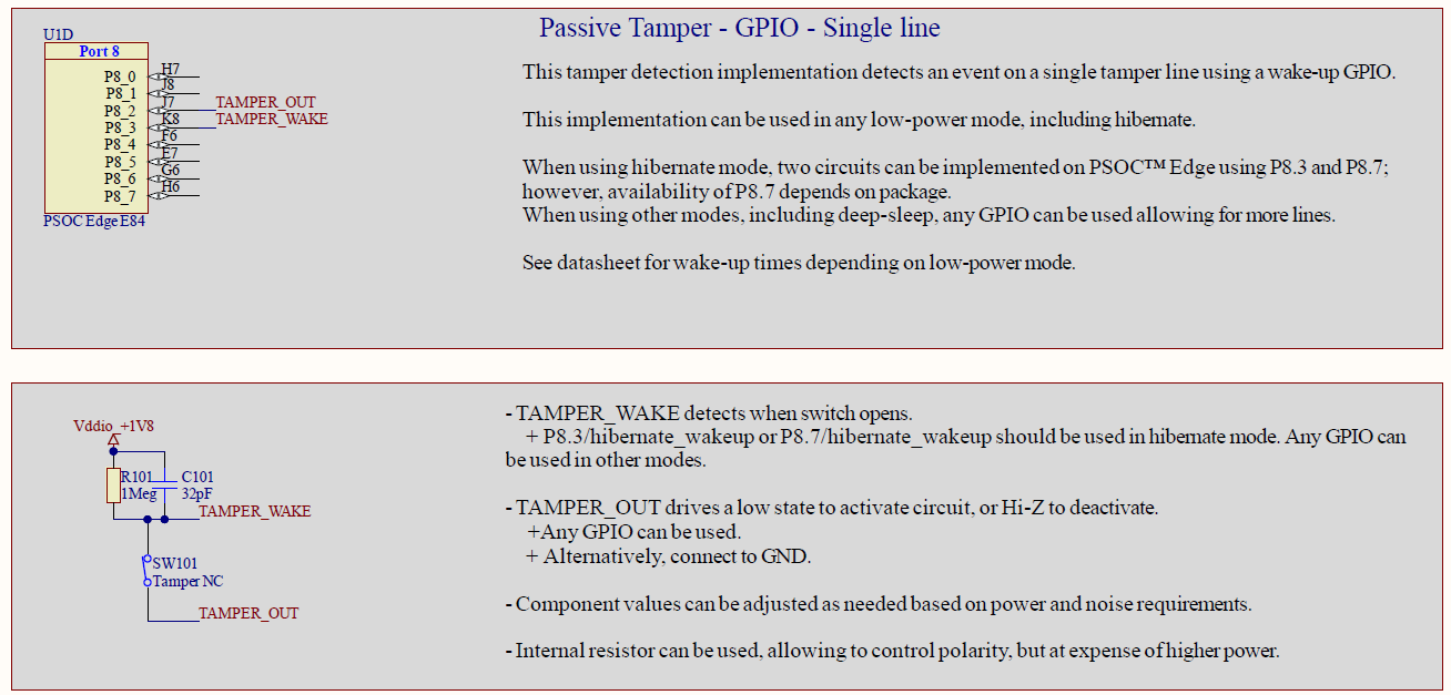
The solution implements a single tamper input line TAMPER_WAKE, which is LOW when idle driven by TAMPER_OUT, or alternatively by a ground signal; and raises HIGH when the switch opens due to an external pull-up resistor.
Given the simplicity of this approach, it only requires one optional output pin, and one input pin with interrupt capability; however, the input pin selection depends on the desired power mode. This approach can be implemented on any PSOC™ active and low power mode, including Hibernate mode; however, the number of pins which can wakeup the device from Hibernate mode are limited. PSOC™ Edge E84 supports two hibernate_wakeup inputs (P8.3 and P8.7), which would allow implementing a maximum of two tamper lines using this approach. On the other hand, PSOC™ Edge supports interrupts and wakeup from practically any I/O pin (except fixed-function I/Os) when using any other mode, including Sleep and Deep Sleep allowing the implementation of as many tamper detection lines as the number of available pins.
Code example
Passive tamper detection of a GPIO requires detecting a basic secure pin interrupt and handling the tamper response event.
ModusToolbox™ includes the
CE241529 – PSOC™ Edge passive tamper detection using LPCOMP
code example, which shows the implementation of tamper line detection using LPCOMP in Hibernate mode in the CM33 secure environment and
CE239674 – PSOC™ Edge MCU: Secure and Non-secure GPIO
shows the implementation of secure GPIO interrupts. These examples provide the building blocks for the detection of a secure GPIO interrupt and how to handle the tamper response.
Power consumption
The power consumption of this implementation depends on three factors:
Device idle power mode: This implementation requires no CPU time when idle since the circuitry will wakeup the CPU only when a tamper event is detected, so the device power consumption when idle is only imposed by the low-power mode. Using Hibernate mode for PSOC™ Edge, power consumption is around 3.33 μW (0.3 μA at 3.3 V + 1.3 μA at 1.8 V). See the Low-power modes for tamper detection applications section for more details about baseline power modes and the impact on power consumption, capabilities, and wake-up times
MCU circuitry: This approach only requires one input and one optional output pin, so the power consumption is only the leakage current, which is practically negligible. See the corresponding datasheet for actual values
Tamper circuitry: The proposed circuit uses a pull-up resistor which will draw current when idle. The current is calculated as , which equates to ; however, it is important to mention that the resistor and capacitor can be adjusted according to the application needs. It is also possible to use an internal pull resistor; however, it can result in higher power consumption. The typical resistance for an internal pull-up/down resistor on PSOC™ Edge is 50 kΩ, which would result in 36 μA at 1.8 V. It is also important to mention that using a NO tamper switch, such as the one shown in Figure 3 would not close the circuit when idle, eliminating this power consumption component
Using the circuitry shown in this application note in Hibernate mode for PSOC™ Edge, the power consumption of the device would be ~3.33 μW. The external circuitry adds ~3.24 μW; however, this component can be adjusted based on application needs.
Response time
The response time of this implementation depends on the following factors:
Tamper detection circuitry:
The proposed circuit uses an RC circuit which will rise when the switch is opened. For the example shown in this application note, the RC constant is calculated as , and since PSOC™ Edge has a VIH of 0.7*VDD, the rise time is approximately ~1.204RC, which is around ~38.5 μs. This time can be adjusted based on the values of the RC circuit
Wakeup time from idle power mode:
Once a logic HIGH is detected, the circuitry will trigger a wakeup event, and the device wakeup time will depend on the power mode being used. In Hibernate mode for PSOC™ Edge, the wakeup time is around ~25 ms with secure boot disabled. See the Low-power modes for tamper detection applications section for more details about baseline power modes and the impact on power consumption, capabilities, and wakeup times
CPU execution:
After waking-up, the CPU will start executing and the time it takes to execute the tamper response routine will depend on the application. It is recommended to optimize initialization functions, such as CINIT and system initialization routines, but since this factor depends on the application, it is not considered for the calculation
As observed, the response time is mostly defined by the wakeup time from idle mode, which is around ~25 ms when using Hibernate mode with secure boot disabled using PSOC™ Edge E84 MCU.
Passive tamper implementation using LPCOMP
A variation of the passive tamper implementation can be implemented with the low power comparator (LPCOMP) available in PSOC™ MCUs.
LPCOMP is an internal comparator which can perform fast analog signal comparison of internal and external analog signals in all system power modes, including Hibernate and Deep Sleep modes. LPCOMP has a programmable operational mode, which can adjust its power consumption and speed, and its output can be used as an interrupt or wakeup source from low-power modes. When used in ultra-low power (ULP) mode of operation, it is a power-efficient way to detect events, even while the device is in Hibernate mode.
Figure 6.
Low-power comparator block diagram
LPCOMP can be used for tamper detection using NC or NO switches; however, this application note describes solutions to detect a single tamper line or multiple using NC tamper switches.
Hardware and device implementation - Single line
LPCOMP can be used to detect a single tamper line as shown in
Figure 7
:
Figure 7.
Schematics for single tamper line passive detection using LPCOMP
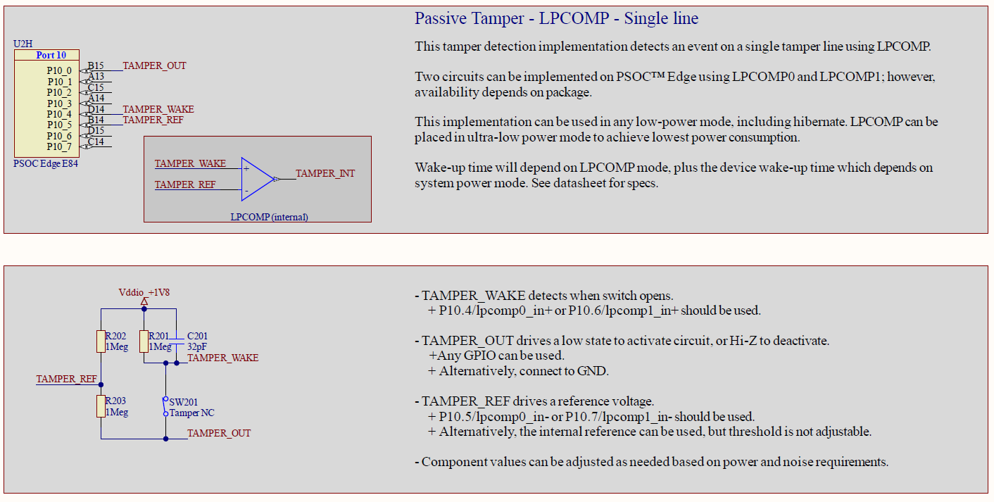
The implementation is similar to the one described in
Passive tamper implementation using GPIOs
; however, the main difference is the use of LPCOMP and an analog reference voltage.
A single tamper input line TAMPER_WAKE is LOW, when idle driven by TAMPER_OUT, or alternatively by a ground signal; and raises HIGH when the switch opens due to an external pull-up resistor. This signal is connected to the positive input of LPCOMP, while an external reference TAMPER_REF is connected to the negative input. The external reference is derived from a voltage divider calculated as
. Note that an internal reference can also be used. For PSOC™ Edge E84 MCU, the internal reference can vary from 0.4 V to 0.8 V.
The LPCOMP output (TAMPER_INT) generates an interrupt or wakeup event internally. The signal can be made available externally if needed.
This solution can be implemented using any active and low-power mode, including Hibernate mode; however, it is limited by the number of LPCOMPs available on the device. PSOC™ Edge E84 MCU includes two LPCOMP modules, but their availability depends on the package.
Hardware and device implementation - Multiple lines
A variation of the previous solution can be implemented to support multiple input lines as shown in
Figure 8
:
Figure 8.
Schematics for passive detection of multiple tamper lines using LPCOMP
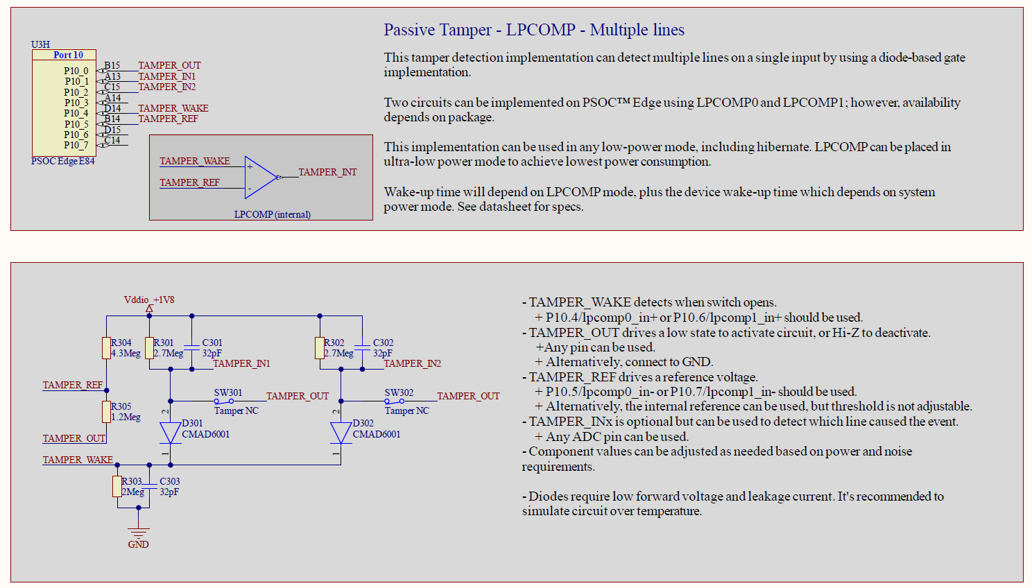
The schematic shows the implementation of two tamper NC switches; however, the same approach can be used to implement more lines if needed.
Similarly to the previous solution, the negative LPCOMP input TAMPER_REF is driven by a voltage divider calculated as
, while the positive input TAMPER_WAKE is normally LOW when the switches are closed, and it gets pulled high when any of the switches open due to external diodes implementing a simple OR gate.
Optional tamper input pins, shown as TAMPER_IN1 and TAMPER_IN2, can be read using an ADC to detect which tamper switch caused the event, but note that using the ADC is only necessary after a tamper event happens, so it will not cause additional power consumption in idle mode.
Diodes with low forward voltage should be used, since the voltage drop will affect the level seen by TAMPER_WAKE. Additionally, the diodes should have a low leakage current to prevent reverse-loading the circuit when one or more switches open.
It is recommended to simulate the circuit to ensure the system will behave correctly over the application's desired temperature range.
Similar to the single-line approach, this solution can also be implemented in any low power mode, including Hibernate mode; and it is also limited by the number of LPCOMPs available on the device, but with the condition that multiple tamper inputs can be implemented on each comparator.
Code example
ModusToolbox™ includes the
CE241529 – PSOC™ Edge passive tamper detection using LPCOMP
code example, which shows the implementation of multiple tamper line detection using LPCOMP in Hibernate mode in the CM33 secure environment.
The example also implements an RTC using the CM33 non-secure environment, waking up the device periodically when the device is idle.
See the README in the code example for more details about running the example and configuration options.
Power consumption
The power consumption of this implementation depends on the following factors:
Device idle power mode:
This implementation requires no CPU time when idle since the circuitry wakes up the CPU only when a tamper event is detected, so the device power consumption when idle is only dictated by the low-power mode. Using Hibernate mode for PSOC™ Edge, power consumption is around 3.33 μW (0.3 μA at 3.3 V + 1.3 μA at 1.8 V). See the Low-power modes for tamper detection applications section for more details about baseline power modes and the impact on power consumption, capabilities, and wakeup times
MCU circuitry:
This approach requires one LPCOMP, one optional output pin, and some optional ADC input pins. The LPCOMP power consumption depends on its operating mode and it is defined in the device datasheet. For PSOC™ Edge E84 MCU, the LPCOMP power consumption in ULP mode is 0.3 μA typical, or 0.54 μW. The ADC is not used when the device is in idle mode, so it is not considered as part of the calculation, and the GPIO leakage current is practically negligible. See the corresponding datasheet for actual values
Tamper circuitry - reference:
The solution shown in this application note uses an external voltage divider for the LPCOMP negative reference. The current of this reference can be calculated as
, which results infor the single tamper circuit, orfor the circuit with multiple lines
Tamper circuitry - input lines:
Each input line has a pull-up resistor which will draw current in idle mode since it is connected to ground through TAMPER_OUT. The power consumption for the single line circuit can be calculated as
, while the circuit with two tamper lines is calculated as
Using the circuitry shown in this application note in Hibernate mode for PSOC™ Edge MCU, the power consumption of the device would be approximately 3.87 μW (3.33 μW for Hibernate mode + 0.54 μW for LPCOMP). The external circuitry would add 4.86 μW (1.62 μW for reference + 3.24 μW for input line) for the single line circuitry; or 2.98 μW (0.59 μW for reference + 2.39 μW for input line) for the example with two tamper lines. Note that these examples are only given as a reference and the components can be adjusted as needed based on the application requirements.
Response time
The response time of this implementation depends on the following factors:
Tamper detection circuitry:
The proposed circuit uses an RC circuit which will rise when the switch is opened. For the single line example shown in this application note, the RC constant (τ) can be calculated as , and since the negative reference is set to 0.5 * VDD (0.9 V), the rise time is approximately ~0.69RC, or ~22 μs. The RC constant for the circuit with two tamper lines can be calculated as , and the negative reference is set to 0.22 * VDD (~0.4 V) so the rise time is approximately ~0.35RC, or ~30 μs. This time can be adjusted based on the values of the RC circuit and the voltage divider
LPCOMP response time:
The response time of LPCOMP depends on its operating mode and it is stated in the device datasheet. For PSOC™ Edge E84 MCU, the LPCOMP response time in ULP mode is 7 μs maximum
Wakeup time from idle power mode:
Once the comparator output toggles HIGH, the circuitry will trigger a wakeup event, and the device wakeup time will depend on the power mode being used. In Hibernate mode for PSOC™ Edge MCU, the wakeup time is around ~25 ms with secure boot disabled. See the Low-power modes for tamper detection applications section for more details about baseline power modes and the impact on power consumption, capabilities, and wakeup times
CPU execution:
After waking up, the CPU will start executing and the time it takes to execute the tamper response routine depends on the application. It is recommended to optimize initialization functions, such as CINIT and system initialization routines, but since this factor depends on the application, it is not considered for the calculation
As observed, the response time of this implementation depends on multiple factors; however, when using Hibernate mode, the wakeup time will dominate. For PSOC™ Edge E84 MCU, the response time would be approximately ~25 ms when using Hibernate mode with secure boot disabled.
Active tamper detection
Active tamper detection, unlike passive tamper detection, has an actively driven signal along with the input detection. The actively driven signal is typically a clock output, or a random sequence of pulses. The tamper detector samples both the active output and an input signal that are connected through a normally closed (NC) tamper switch. If both signals are matching, then no tamper has occurred, if the tamper switch has been broken the signals will not match and the tamper should be detected.
Smart I/O
The PSOC™ Edge device has two I/O ports supporting Smart I/O. Smart I/O adds programmable logic to an I/O port. This programmable logic can be used to generate signals and make logical comparisons. The Smart I/O on the PSOC™ Edge device will remain operational in Deep Sleep mode.
The Smart I/O programmable logic is comprised of a data unit (DU), eight look-up-tables (LUT), signal routing, a high-speed I/O matrix (HSIOM), and I/O port input/output signals. The LUTs can be configured for combinatorial logic, gated input, gated output, or S/R flip-flop. The Smart I/O can be used in asynchronous mode, or a clock can be provided to the Smart I/O for programmable logic that requires synchronous logic.
Figure 9.
Block diagram of Smart I/O
Simple PWM active tamper implementation using Smart I/O
One approach for active tamper detection using the Smart I/O fabric is a simple PWM active tamper detection circuit. The LUTs are used to generate a PWM on a tamper output signal. Then a tamper input signal connected to the tamper output signal through an NC switch is compared using the LUTs. The output of this comparison is made available as a tamper status signal, which can be used by the device as an interrupt to wake-up the device and indicate that a tamper event has occurred.
Hardware and device implementation
The schematics for the simple PWM active tamper solution are shown in
Figure 10
:
Figure 10.
Schematics for active tamper detection of four lines using simple PWM with Smart I/O
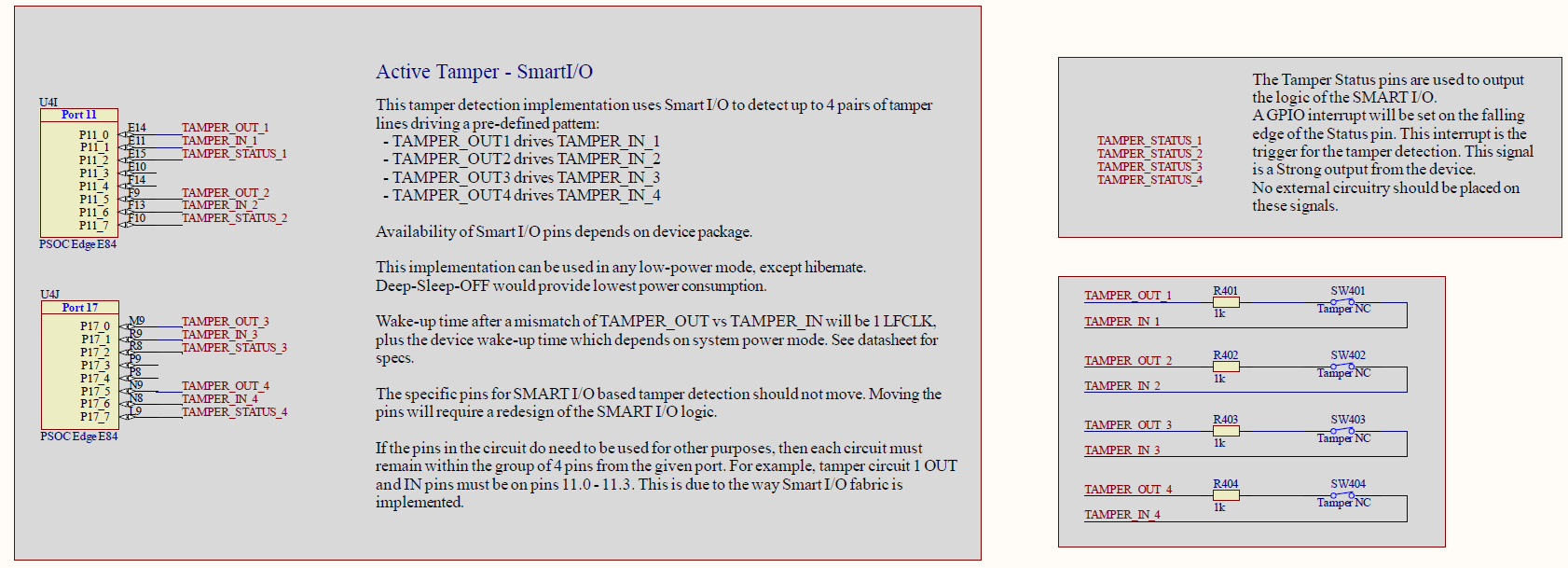
By using the gated output configuration, a D flip-flop or a T flip-flop can be created. In combinatorial mode, an N-XOR and an OR logic gate can be configured. These will be the building blocks for a simple PWM active tamper detection circuit. The low frequency clock (CLK_LF), which runs off of the PILO, WCO, or an ECO, will be used as it is enabled in system Deep Sleep mode.
The PWM is generated by toggling a signal using a T flip-flop. Since the T flip-flop is clocked by the CLK_LF, the PWM will run at 32.768 kHz, which is the frequency of the CLK_LF.
The TAMPER_OUT (PWM) is compared to the TAMPER_IN (asynchronous input) using an N-XOR logic gate. The output of that gate is fed into a D flip-flop to store an "N-1" sample of the comparison. The output of the N-XOR and the D flip-flop (N-1) are fed into a logical OR gate. The output of the OR gate is the TAMPER_STATUS. When the TAMPER_OUT and TAMPER_IN signals do not match for two samples, then TAMPER_STATUS is driven low indicating a tamper event.
Figure 11.
Simple PWM active tamper detection logic
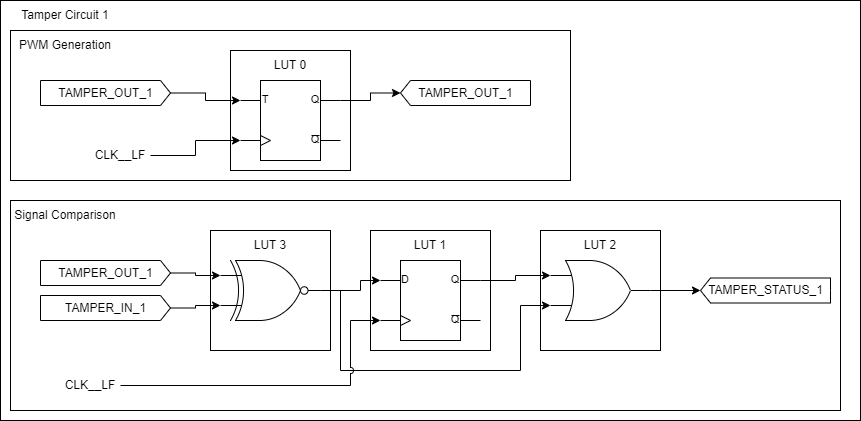
A falling edge GPIO interrupt can be enabled on the TAMPER_STATUS GPIO signal to wake the CPU up to allow it to complete the appropriate steps for a tamper event.
Since this simple PWM active tamper circuit only utilizes three I/Os and four LUTs, it can be duplicated in a given Smart I/O to create two active tamper detection circuits. PSOC™ Edge supports Smart I/O on two ports, so a total of four active tamper pairs can be created.
Code example
ModusToolbox™ includes the
CE241499 – PSOC™ Edge active tamper detection using Smart I/O
code example, which shows the implementation of a single tamper detection circuit implemented on each Smart I/O port in Deep Sleep-OFF mode in the CM33 secure environment.
The example also implements an RTC using the CM33 non-secure environment, waking up the device periodically when the device is idle.
See the README in the code example for more details about running the example and configuration options.
Power consumption
The power consumption of this implementation depends on two factors:
Device idle power mode:
This implementation requires no CPU time when idle since the Smart I/O output will trigger an interrupt, which will wake the device from low-power mode only when tamper is detected. Using System Deep Sleep-OFF mode for PSOC™ Edge MCU, the power consumption is around 108.24 μW (25.0 μA at 3.3 V + 14.3 μA at 1.8 V). See the
Low-power modes for tamper detection applications
section for more details about baseline power modes and the impact on power consumption, capabilities, and wakeup times
MCU circuitry - GPIOs:
This approach only requires one input, one output pin, and one status pin, so the power consumption is only the leakage current, which is practically negligible. See the corresponding datasheet for actual values
MCU circuitry - CLK_LF:
This approach uses the CLK_LF to clock the Smart I/O programmable logic. The CLK_LF can be driven by the WCO, ECO, or the PILO. The WCO is the most efficient of these options and has a typical power consumption of 120 nA. See the corresponding datasheet for actual values
MCU circuitry - Smart I/O:
This approach uses Smart I/O on ports 11 and 17. The Smart I/O is integrated into the GPIO port, so the utilization of the Smart I/O logic consumes very little power. With this example, it is measured to increase the power consumption on VDD (1.8 V) by 1 μA per Smart I/O enabled. See the corresponding datasheet for actual values for the Smart I/O logic
Using the circuitry shown for this active tamper detection solution in Deep Sleep-OFF mode for PSOC™ Edge MCU, the power consumption of this device would be 112.5 μW (25.2 μA at 3.3 V + 16.3 μA at 1.8 V).
Response time
The response time of this implementation depends on the following factors:
Phase of clock when tamper occurred:
The CLK_LF operates at 32.768 kHz. The design requires that the output and input signals are mismatched for two samples, where one sample is taken every clock pulse, while the other is taken asynchronously. The worst case scenario for the Smart I/O fabric to detect and output that tamper has been detected onto the status output signal is ~61 μs. This includes the n-1 sample time (30.5 μs), and the time for the output signal to change from LOW to HIGH, or HIGH to LOW (30.5 μs)
Wake-up time from idle power mode:
Once a falling edge of the tamper status signal triggers an interrupt, the device will wakeup. The wakeup time depends on the idle power mode being used. In system Deep Sleep-OFF mode for the PSOC™ Edge MCU, the wakeup time is around ~25 ms with secure boot disabled. See the
Low-power modes for tamper detection applications
section for more details about baseline power modes and the impact on power consumption, capabilities, and wakeup times
CPU execution:
After waking-up, the CPU will start executing and the time it takes to execute the tamper response routine depends on the application. It is recommended to optimize initialization functions, such as CINIT and system initialization routines, but since this factor depends on the application, it is not considered for the calculation
As observed, the response time is mostly defined by the wakeup time from idle mode, which is around ~25 ms when using Deep Sleep OFF mode with secure boot disabled using PSOC™ Edge E84 MCU.
Alternative tamper detection implementations
The previous examples showed a few options to implement low-power, efficient and effective, tamper detection solutions using PSOC™ microcontrollers. Nevertheless, a wide range of alternative approaches can be used to implement both passive and active tamper detection mechanisms, offering designers flexibility and versatility in their solutions.
Tamper detection using communications peripherals
Serial interfaces such as UART or SPI can be used to send known or randomized patterns, which are compared upon reception.
Figure 12.
Tamper detection using serial communication peripherals
This solution could allow for complex patterns with adjustable frequency and it could allow the implementation of multiple tamper lines (PSOC™ Edge E84 includes 12 SCBs supporting I2C, UART, or SPI); however, it is important to remark that this solution requires CPU time to compare the signal upon reception, a tamper event would only be detected after a whole frame is transmitted and received, and not all low-power modes are possible.
PSOC™ Edge E84 MCU includes one low-power SCB which can be used in Deep Sleep mode. This SCB could be used together with Smart I/O to implement a SPI slave solution as shown in
Figure 13
:
Figure 13.
Tamper detection using SCB-SPI and Smart I/O
In this solution, Smart I/O is used to generate a clock output, which is connected externally to the SPI_CLK input. CPU or DMA can be used to load patterns into the SPI FIFO, which will be sent using SPI_MISO, while the same signal is received back if the tamper NC switch is closed. If a tamper event occurs, the line will open and the received data will mismatch.
Compared to the Smart I/O solution discussed in
Simple PWM active tamper implementation using Smart I/O
, this approach requires fewer Smart I/O LUTs and pins, which could be used for other purposes; however, this solution is expected to consume more power, especially since it requires continuous DMA and/or CPU intervention.
Tamper detection using autonomous analog
The autonomous analog module is a block that integrates programmable opamps (CTB), which can perform a variety of analog front-end functions, DACs, ADCs, comparators, programmable reference blocks (PRB), and digital-post processors. These blocks are controlled by a CPU-independent state machine called the "autonomous controller". The autonomous controller is operable in system Deep Sleep mode, which allows the system to monitor analog components, and gather and pre-process data at a very low power consumption.
Figure 14.
Autonomous analog block diagram
A tamper detection solution could be implemented using the autonomous analog DAC and either ADC or comparators as follows:
Figure 15.
Tamper detection using autonomous analog
The DAC can be configured to output a constant voltage, which is compared without CPU intervention using the ADC's limit detection feature, or by using a programmable threshold comparator (PTComp). The autonomous analog has two DACs, which could allow to implement up to two output signals, but it supports up to 16 ADC pins and two PTComps, which could allow for multiple tamper input lines.
Alternatively, an active tamper approach could be implemented by generating a pattern using the DAC automatic waveform generator, which could be compared by a pair of PTComps in window comparator mode and using the comparator post-processing unit. The output pattern could optionally be randomized periodically with CPU intervention.
As mentioned earlier, the autonomous analog block can be used in system Deep Sleep mode for PSOC™ Edge MCU, which allows for a low-power implementation with no CPU intervention; however, the power consumption of the autonomous analog module should be considered.
Tamper detection using timers
PSOC™ MCUs include a variety of timers which could be used to generate a known or randomized active pattern.
Figure 16.
Tamper detection using timers
PSOC™ Edge E84 MCU includes up to 32 timer, counter and pulse width modulator (TCPWM) modules, out of which eight have 32‑bit counters, and 24 have 16‑bit counters. The counter can be used to measure the period and pulse width of an input signal (timer), find the number of times an event occurs (counter), generate PWM signals, or decode quadrature signals.
An active tamper solution could be implemented by generating a known pattern and using counter mode to count the number of received edges. The CPU would periodically check the number of received edges and compare with the expected value. The pattern could also be randomized periodically using CPU intervention; however, software and more CPU cycles would be required to re-calculate the number of expected edges.
One advantage of this solution is that it could allow to implement many different tamper lines with potentially very fast and complex patterns; however, it requires CPU intervention to compare the number of received edges and/or modify the pattern; a tamper event is not detected immediately but after the CPU wakes-up to compare the number of edges; and, the timers might not be available in all power modes. On PSOC™ Edge MCU, the TCPWM can be used in Active and Sleep mode, which would make this solution more feasible for non-battery operated applications.
Using random generators
The solutions mentioned in this document show how to implement a passive tamper approach, or an active approach using a known pattern; however, it is also possible to leverage PSOC™ hardware to generate random patterns.
In addition to software mechanisms, PSOC™ Edge MCU includes a true random generator (TRNG) and a pseudo random number generator (PRNG), each with a programmable size up to 32-bits.
These generators can be used to randomize the output patterns for active tamper solutions presented in this document.
Tamper response mechanisms
Tamper response is a critical component of secure system design. In the context of embedded systems, tamper response refers to the mechanisms and strategies employed to react to tampering events, such as physical intrusion, software manipulation, or data breaches. A well-designed tamper response system is essential for protecting sensitive information, preventing intellectual property theft, and ensuring the integrity of critical infrastructure.
An effective tamper response involves a combination of hardware and software counter measures that work together to respond to potential security threats, and it can vary depending on the application needs. While some applications might require to report a tamper event with an alarm or notification, other applications might require to reset the device, enter in a fail-safe mode, erase sensitive data, or completely erase the application.
This application notes discusses two methods which leverage the high security mechanisms of PSOC™ Edge MCUs: erasing keys using Secure Enclave, and changing the device lifecycle to RMA.
Erasing keys using SE RT services
PSOC™ Edge devices include a Secure Enclave (SE), which includes two Cortex® M0+ CPUs operating in delayed lock-step. The Secure Enclave is responsible for the initial secured boot and the root of trust, and it also provides a range of security functions, maintains storage for secure keys, and performs security key management. These functions are implemented in the Secure Enclave run-time services (SE RT) library, which is only available for EPC 4 devices.
Note that it is possible to store and erase keys in internal or external user memory using EPC 2 or EPC 4 devices; however, this application note focuses on how to leverage the SE RT services available on EPC4 devices to achieve maximum security by using the Secure Enclave.
To get access to the SE RT services, the application needs to include the SE RT services utilities library using the ModusToolbox™ Library Manager and including
ifx_se_psacrypto.h
. Once added, the following functions can be used to generate and delete keys:
ifx_se_generate_key:
Generates a key or key pair. The key is generated randomly. Its location, usage policy, type, and size are taken from the "attributes" parameter
ifx_se_destroy_key:
Destroy a key. This function destroys a key from both volatile memory and non-volatile storage. This function also erases any metadata such as policies and liberates resources associated with the key
Considering the flow diagram shown in
Figure 17
, the application flow to erase keys can be complemented as follows:
Figure 17.
Flow diagram for tamper response by erasing keys using RT services
Note that this application note implements the tamper response routine in CM33 secure code, making it independent of the non-secure projects. This approach also only shows how to use SE RT services to erase keys, assuming they are the most sensitive data in the device; however, the application remains functional and developers can perform other actions as needed, such as logging or reporting the event, or erasing memory.
Handling volatile keys
An additional layer of protection can be implemented by leveraging the volatile backup registers (BREG) to chain-encrypt secrets only while the device is powered, and losing the key automatically when the battery is removed.
PSOC™ Edge contains multiple backup registers, which are retained in all power modes, including System Hibernate and System Deep Sleep-OFF. These registers can be used to chain-encrypt secrets as follows:
Define the size of the protected assets
Generate on-die random AES 256-bit key during provisioning. Store it in BREG and protect access
Receive/generate the protected assets using Secure Enclave
Encrypt assets using the AES key in BREG
Store the encrypted assets in Secure Enclave storage
To use assets:
Decrypt assets using Secure Enclave and the AES key in BREG
The AES key will remain in BREG even if the device goes in and out of low power modes
If the power supply to the system is interrupted, the AES key stored in BREG will be lost. As a result, any stored assets that were encrypted using this key will become inaccessible, as there will be no available key to decrypt them. However, to provide an additional layer of security, the Secure Enclave storage has been designed to be resilient against invasive attacks.
Note that in this scenario, the system will stop being fully functional if the AES keys are lost due to a power interruption, and will need to undergo a re-provisioning process.
RMA lifecycle
While the earlier solution focuses on erasing specific sensitive data, a more drastic approach can be implemented by changing the lifecycle of the device.
As mentioned in the
Authenticated debug
section, PSOC™ Edge MCU supports three device lifecycle stages (LCS) relevant to product developers: development, production, and RMA.
An application can decide to change the lifecycle of the device to RMA if tamper is detected, effectively deleting all data and stopping the application.
Considering the application flow diagram shown in
Figure 4
, the flow to change LCS to RMA would be as follows:
Figure 18.
Flow diagram for tamper response by changing lifecycle to RMA
This approach requires generating a device reset to initiate the lifecycle change, so it is recommended to prioritize erasing sensitive data before changing the lifecycle to RMA.
Note that once a device is transitioned to the return merchandise authorization (RMA) stage, it will be rendered inoperable and cannot be restored to a previous stage in its lifecycle.
ADC
analog-to-digital converter
BSP
board support package
CLK_LF
low frequency clock
COMP
comparator
CTB
continuous time block
CRC
cyclic redundancy check
DAC
digital-to-analog converter
DMA
direct memory access
DPA
differential power analysis
DU
data unit
ECO
external crystal oscillator
EPC
edge protect category
EVK
evaluation kit
FIFO
first in, first out
FSM
finite state machine
GPIO
general purpose input/output
HSIOM
high-speed I/O matrix
I2C
inter-integrated circuit
JTAG
Joint Test Action Group
LCS
lifecycle stage
LP
low power
LPCOMP
low-power comparator
LUT
look-up table
LVD
low-voltage detect
MCU
microcontroller
MMIO
memory-mapped I/O
NC
normally closed
NO
normally open
NSPE
non-secure processing environment
OEM
original equipment manufacturer
OVD
overvoltage detect
PILO
precision internal low-speed oscillator
POR
power-on reset
PRB
programmable reference block
PRNG
pseudo random number generator
PSA
Platform Security Architecture
PTComp
programmable threshold comparator
PWM
pulse-width modulation
RC
resistor-capacitor
RMA
return merchandise authorization
RRAM
Resistive RAM
RoT
root of trust
RT
runtime
RTC
real-time clock
SAR
successive approximation register
SCA
side-channel attacks
SCB
Serial Communication Block
SE
Secure Enclave
SE_RT
Secure Enclave runtime
SMIF
Serial Memory Interface
SPE
secure processing environment
SPI
serial peripheral interface
SWD
Serial Wire Debug
TCPWM
timer/counter pulse-width modulator
TRNG
true random number generator
ULP
ultra-low power
WCO
watch crystal oscillator
WCO
WDT
watchdog
XIP
Execute in Place
Revision history
Document revision | Date | Description of changes |
|---|---|---|
** | 2025-10-03 | Initial release |
Trademarks
PSOC™, formerly known as PSoC™, is a trademark of Infineon Technologies. Any references to PSoC™ in this document or others shall be deemed to refer to PSOC™.