AN239527 PSOC™ Control C3 MCU hardware design guide
About this document
Scope and purpose
This application note describes how to set up a hardware environment for
PSOC™ Control C3
family. This application note discusses considerations for hardware design including package, power, clocking, reset, I/O usage, programming/debugging, and the respective PCB layout considerations.
Intended audience
This application note is intended for hardware designers.
Introduction
The PSOC™ Control C3 family is designed for real-time control, enhanced sensing, secure, and low-power operations. Some target applications for these MCUs are:
The
PSOC™ Control C3
device must be configured to work in the intended hardware design. This can be done with an integrated development environment (IDE) like
ModusToolbox™
.
Package selection
One of the first decisions you must make for your PCB is the choice of package. Several considerations drive this decision, including the number of I/O pins required, PCB and product size, PCB design rules, and thermal and mechanical stresses. The PSOC™ Control C3 MCU family has a large selection of packages to match your exact needs with an efficient and cost-effective solution. Package offerings comprise the compact VQFN package and the E-LQFP package which is easier to layout on lower layer counts and low-cost PCBs.
Package | Pins |
|---|---|
VQFN | 48-pin |
64-pin | |
E-LQFP | 48-pin |
64-pin | |
80-pin |
Power
The PSOC™ Control C3 can be powered by a single supply with a wide voltage range, from 1.71 V to 3.6 V. The MCU power system is based on separate analog and digital supplies as listed in Table 1.
Figure 1.PSOC™ Control C3 typical power supply connections (LQFP-80)
Figure 1 shows a typical powering scheme for the 80-pin LQFP package. See the device datasheet for details about other pin packages. Details of connections to the power pins are described in the Power pin connections section.
Power domains
Power domain | Associated pins |
|---|---|
Analog | VDDA |
Digital | VCCD |
I/O | VDDIO0, VDDIO1 |
Shared digital and I/O | VDDD, VBACKUP |
Pin name | Function | Nominal power domain voltage range |
|---|---|---|
VDDD | Shared power supply pin for internal voltage regulators, internal logic, I/O domain, and debug interface. | 1.71 V to 3.6 V |
VCCD | Only used to connect an external bypass capacitor for the integrated core logic supply LDO outputs. Note: Do not connect any external supply or use this pin to power external components. | 0.9 V to 1.2 V |
VBACKUP | Backup domain power supply including the backup domain I/O cells. Can be connected to a coin cell or a super capacitor depending on the application. If not used, it should be connected to VDDD. | 1.4 V to 3.6 V |
VDDA | Powers the analog domain circuits | 1.71 V to 3.6 V |
VDDIO0, VDDIO1 | Power supply for the I/O cells | 1.71 V to 3.6 V |
Power pin connections
shows the power pin connections and routing block diagram. All the power pins can be connected together to a single regulated supply between 1.71 V to 3.6 V. When using a single supply source, place ferrite beads for minimizing the noise interference between analog and digital supply inputs. Alternatively, it is possible to use independent regulated supplies for all power input pins within their valid operating voltage range. For device-specific details including pin information, see the
device datasheet
.
Figure 2.
Power distribution and domains
Core regulators
The device features multiple low drop-out (LDO) regulators that are responsible for powering the device in the supported power modes. All the core regulators draw power from the VDDD supply and generate a voltage ranging between 0.9 V to 1.2 V. The VDDD supply needs to be a stable voltage ranging between 1.71 V to 3.6 V and bypassed with capacitors as per the values specified in the
Figure 2
. Bypass capacitors should be placed as close as possible to the device supply pins.
The LDO output is connected to the VCCD pin with the sole purpose of connecting an external bypass capacitor.
Note: The bypass capacitors should be of X5R type or better.
Power ramp-up considerations
The device has no special power-on and ramp-up considerations. The power-on reset (POR) circuit on the VDDD and internal VCCD supply ensures that the device has a stable power supply before deasserting the reset. If backup functionality is not used, connect VBACKUP to VDDD. Other pins used for I/O and analog supply can be left unconnected if the associated sections are not used in the application. The device enters Active mode by default after power-on.
Note: VDDIO supply on/off state change is only allowed in Active, Sleep, and Deep Sleep modes. It should not be changed in Hibernate mode.
Clocking
The device supports the following clock sources:
Internal main oscillator (IMO): 8 MHz ±2%, fast wakeup, low jitter
Internal high-speed oscillator (IHO): 48 MHz ±1%
Internal low-speed oscillator (ILO): 32 kHz ±10%, also as a wakeup source for the RTC
External crystal oscillators (ECO and WCO)
External crystal oscillator (ECO): 4 MHz to 35 MHz
External watch crystal oscillator (WCO): 32.768 kHz
External clock (EXTCLK): Maximum frequency 80 MHz
One frequency lock loop (FLL) with 24 MHz to 100 MHz output range
Two digital phase-locked loops, DPLL#0 and DPLL#1, with 25 MHz to 250 MHz output range
CLK_HF | Peripherals | Recommend source | Max permitted clock frequency 1 | |||
|---|---|---|---|---|---|---|
OD (1.2 V) | LP (1.1 V) | MF (1.0 V) | ULP (0.9 V) | |||
CLK_HF0 | CPU, PERI, SRSS, CORDIC, CRYPTO | DPPL0 | 180 MHz | 150 MHz | 70 MHz | 50 MHz |
Peri clock group 0 (Debug trace) | 90 MHz | 75 MHz | 35 MHz | 25 MHz | ||
CLK_HF1 | IOSS, LPCOMP, Peri clock group 1 (SMARTIO) | DPLL0 | 180 MHz | 150 MHz | 70 MHz | 50 MHz |
CLK_HF2 | Peri clock group 4 (CAN, SCB[0:4]) | FLL | 100 MHz | 100 MHz | 25 MHz | 25 MHz |
CLK_HF3 | HPPASS 2 , Peri clock group 5 (TCPWM, HPPASS CSG) | DPLL1 | 240 MHz | 200 MHz | 120 MHz | 60 MHz |
CLK_HF4 | Peri clock group 6 (SCB[5]) | DPLL1 (For fast SPI) | 240 MHz | 200 MHz | 120 MHz | 60 MHz |
FLL (For UART/I2C) | 100 MHz | 100 MHz | 25 MHz | 25 MHz | ||
CLK_HF5 | EXT_CLK_OUT | All | 80 MHz | 80 MHz | 80 MHz | 50 MHz |
CLK_HF6 | CSV | All | 8 MHz | 8 MHz | 8 MHz | 8 MHz |
Use the recommended clock source for the respective CLK_HF domains.
External crystal oscillator (ECO)
The device can be clocked using the external crystal oscillator (ECO). A crystal of 4 MHz to 35 MHz connected to the ECO_IN (P1.0) and ECO_OUT (P1.1) pins of the device is used to generate the clock. When using the ECO, it needs to be enabled. This can be done using Device Configurator in ModusToolbox™. To minimize the stray capacitance, the crystal along with associated components are placed on the same layer as the MCU and close to the device pins.
Figure 3.
ECO connections
The external load capacitors for the ECO are calculated as:
C = 2 × (CL−CS) − C P
where,
C
L
: Crystal load capacitor as per the crystal datasheet.
C
S
: PCB stray capacitance. A well-designed PCB minimizes the stray capacitance and includes a grounded copper trace between the crystal input and output wires.
C
P
: Package pin-to-ground parasitic capacitance (see the
device datasheet
for more details on pin parasitic capacitance).
Watch crystal oscillator (WCO)
The watch crystal oscillator (WCO) block requires an external 32.768 kHz crystal connected between WCO_IN (P0.1) and WCO_OUT (P0.0) along with input and output load capacitors for proper operation.
Figure 4.
WCO connections
The external load capacitors for the WCO are calculated as:
C = 2 × (CL−CS) − CP
where,
C
L
: Crystal load capacitor as per the crystal datasheet
C
S
: PCB stray capacitance. A well-designed PCB minimizes the stray capacitance and includes a grounded copper trace between the crystal input and output wires.
C
P
: Package pin-to-ground parasitic capacitance (See the device datasheet for more details on pin parasitic capacitance).
External clock
The external clock is a 0.001 MHz to 80 MHz range clock that can be sourced from a signal on pin P0.0 or P2.2. This clock can be used as the source clock for either the DPLL or FLL, or can be used directly by the high-frequency clocks.
Clock supervisor output
A clock supervision (CSV) circuit is implemented for each clk_hf domain. The CSV circuit detects a stopped clock or an abnormal frequency of the monitored clock. There are clock counters for both the monitored clock and the reference clock. Parameters for each counter define the frequency of the reference clock and the upper and lower limit for the frequency of the monitored clock.
If the dedicated frequency range comparator detects a stopped clock or a clock outside the specified frequency range, an abnormal state is signaled. Depending on the register settings and how the monitored clock is used on the device, either a reset or an interrupt is generated.
1
Maximum clock frequency after the corresponding clock source (DPLL/FLL + dividers). All internal tolerances and affects are covered by these frequencies.
2
The minimum permitted clock frequency of HPPASS is 60 MHz.
Reset
XRES
The PSOC™ Control C3 has a reset pin (XRES) that is active LOW. XRES should be externally pulled up to VDDD via a 4.7 kΩ resistor. This will make sure that the XRES pin is not left floating in the design and that the device can function properly. It is recommended to connect a capacitor (typically 0.1 µF) to the XRES pin to filter out glitches and give the reset signal better noise immunity. Optionally, if the device is controlled by an external host, the XRES pin can be directly driven by the host.
Power supply monitoring
To make sure that the MCU is not running outside the valid operating conditions, a broad range of power monitor circuits are provided within the MCU. See the
device architecture reference manual
and
datasheet
for more details.
Power-on reset (POR)
Power-on reset (POR) circuits provide a reset pulse during the initial power ramp. At the system level, only the VDDD power supply rail is observed.
Brown-out detection (BOD)
The brown-out detection (BOD) circuit protects the operating or retaining logic from possibly unsafe supply conditions by applying reset to the device. BOD circuits for the power supply rails VDDD and VCCD are provided. A reset is generated when an out-of-range condition is detected on the monitored voltages. This circuit is required to detect a sneaking voltage drop of the battery power supply.
Low voltage detection (LVD)
Before the BOD level threshold generates a reset, it is possible to get a low voltage detection (LVD) warning by the configurable circuit. The LVD trip point can be configured by writing to the PWR_LVD_CTL register. When the trip threshold is triggered, LVD generates a CPU interrupt for possible safety measures. By default, LVD is disabled because it consumes power; it must be enabled if used by the application.
Watchdog reset
An internal watchdog timer (WDT) and multi-counter watchdog timer (MCWDT) support a wide range of capabilities. They can be configured to reset the device in case of software faults which halt code execution.
GPIO pins
GPIO pins
The
PSOC™ Control C3
provides flexible GPIO pins. All GPIO pins can be controlled by firmware. Most of them also have alternative connections to the
PSOC™ Control C3
peripherals. Different peripherals have different dedicated or fixed pins for their terminals. You get the best performance when a peripheral is connected to its own dedicated pin or pins. However, for flexibility, you can connect the peripheral to other pins using the high-speed I/O matrix (HSIOM). The flexibility of
PSOC™ Control C3
devices and the capability of its I/O to route most signals to most pins greatly simplify circuit design and board layout. If a peripheral has fixed pins, you can connect it only to those pins. For more information on the pinout and the pin alternate functionality, see the
device datasheet
.
I/O pin selection
When you design a hardware system based on the
PSOC™ Control C3
, the GPIO pins should be assigned in sequence as shown in the following table. See the
device datasheet
to determine whether the listed peripheral block is supported by the device.
Block | Pin name | Port#[Pin#] | Remarks |
|---|---|---|---|
System function pins | |||
Run-time debug | If you need run-time debugging or trace support, select the appropriate setting in the System settings. The selection will automatically lock the required I/Os for the purpose. | ||
External crystal oscillator (ECO) | ECO_IN | P1.0 | External crystal frequency range: (4 MHz – 35 MHz) |
ECO_OUT | P1.1 | ||
Watch crystal oscillator (WCO) | WCO_IN | P0.0 | If you need a highly accurate and low-frequency clock for RTC or Deep Sleep wakeup purpose, use the WCO block with an external 32.768 kHz crystal or clock. Note that the WCO block is present in the device’s backup domain and it is available, even when the VDDD of the device is removed (VBACKUP supply shall be present). |
WCO_OUT | P0.1 | ||
Wakeup (Hibernate) | HIB_WAKEUP | P2.0 or P9.0 | The Hibernate wakeup pin is used to wake the PSOC™ Control C3 from Hibernate mode. |
External clock | EXT_CLK | P0.0 or P2.2 | Configure the pin as an input (high impedance digital) for receiving the external clock. |
Analog pins | |||
Low-power comparator | LPCOMP0_IN+, LPCOMP1_IN+ | P8.0, P8.2 | Non-inverting [+] and inverting [-] inputs for the two low-power comparators |
LPCOMP0_IN-, LPCOMP1_IN- | P8.1, P8.3 | ||
ADC analog input pins | Analog inputs directly connected to dedicated samplers | AN_A0 to AN-A7 and AN_B0 to AN_B3 | Pins supporting ADC functionality |
Analog inputs connected through AMUX | B4 to B7, P8.0, P8.2 | ||
Digital pins | |||
Timer/counter pulse-width modulator (TCPWM) | TCPWM pins | See the device datasheet | PSOC™ Control C3 has up to 20 TCPWM blocks with each block having two complementary outputs. All the output signals can be routed to any GPIO pin by either using the alternate functionality or by using peri.tr_io_output via the HSIOM. |
Serial communication block (SCB) | SCB pins | See the device datasheet | PSOC™ Control C3 devices have up to six SCBs out of which SCB0 is capable of working in Deep Sleep mode for SPI and I2C. Some devices feature fast SPI capability for SCB5. See the device datasheet for the device-specific capabilities. |
Open pin connection
During and after a POR, by default, the I/O pins are in a high-impedance (High-Z) analog state with disabled input buffers. The advantage of leaving unused I/O pins open is that the current consumption of the MCU is lower when compared to the use of a terminal resistor; this also reduces the BOM cost. PCB designers need to ensure that the trace length of unused pins is short to avoid the unused trace from acting like an antenna and picking up noise. If any pin is routed for future expansion options, it is recommended to place a 0 Ω resistor close to the pin and keep it unmounted as long as the pin is not in use.
Direct connection to GND or power supply
The I/O pins should not be connected directly to GND or to power supply because the power supply traces can take effect as an antenna to the pin and the captured noise can cause a latch-up effect.
Programming and debugging
The
PSOC™ Control C3
program and debug interface provides a communication gateway for an external device to perform programming or debugging. The external device can be an Infineon-supplied programmer and debugger or a third-party device that supports programming and debugging. The Serial-Wire Debug (SWD) or the JTAG interface can be used as the program/debug protocol between the external device and the PSOC™ Control C3. In addition, the PSOC™ Control C3 supports Arm® Embedded Trace Macrocell (ETM) on the Cortex®-M33 CPU.
SWD
For SWD programming or debugging, you can use the onboard programmer/debugger in the MCU kits when available, or connect the device to an external debugger such as
CY8CKIT-005-A
MiniProg4 via any connector supported by the debugger. MiniProg4 supports a 10-pin and a 5-pin connector for SWD programming and debugging. The VTref voltage should be connected to the same voltage as the VDDIO voltage of the SWD interface pins. This voltage is used by the onboard or external debugger to set the logic voltage level for the SWD signals.
Figure 5.
10-pin Cortex® debug connector

Figure 6.
SWD debug connection to the MCU with 10-pin MIPI SWD debug connector
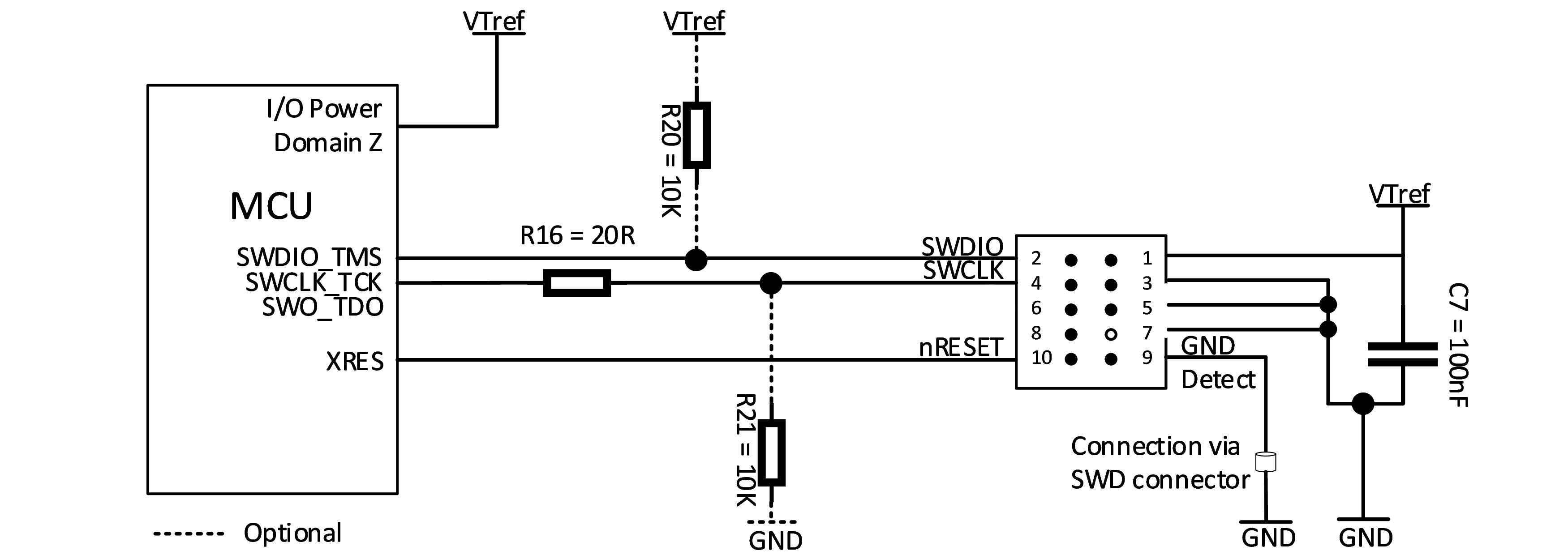
From
Figure 6
, it can be seen that the minimum of four connections (two SWD pins, GND, and VTref) are needed from the target board to the debugger in SWD mode.
JTAG
For JTAG programming and debugging, external debuggers like MiniProg3 or J-Link can be used. Both 4-wire and 5-wire JTAG programming is supported in PSOC™ Control C3.
Note: JTAG is disabled by default and needs to be enabled in the OEM policy.
Embedded Trace Macrocell (ETM)
The Cortex®-M33 CPU in
PSOC™ Control C3
supports parallel trace mode with 1, 2, and 4 data lines.
Figure 7.
20-pin Cortex® debug + ETM connector
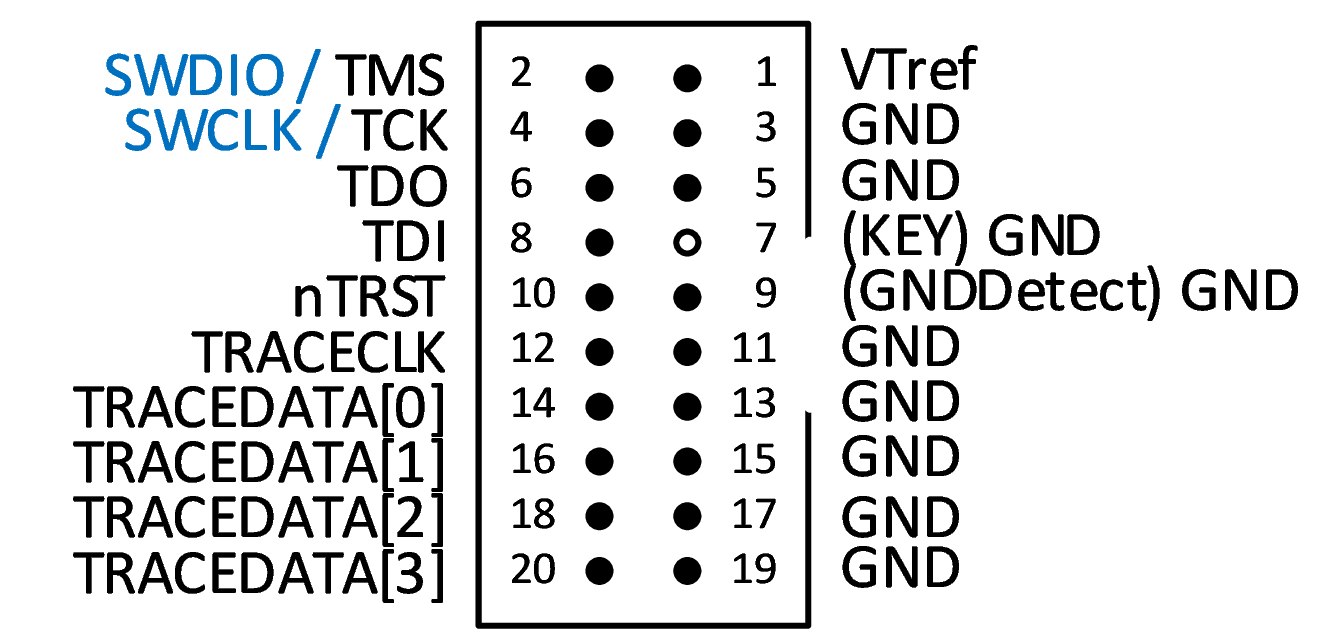
Pin | Name | Functionality |
|---|---|---|
1 | VTref | Target reference voltage. Used by the external debugger/trace tool to set the logic voltage level for communication. |
2 | SWDIO/TMS | SWD interface data pin/JTAG TMS pin |
3 | GND | Ground |
4 | SWCLK/TCK | SWD clock/JTAG clock |
5 | GND | Ground |
6 | TDO | JTAG TDO pin |
7 | (KEY) GND | No pin on the header. Connected to the ground. |
8 | TDI | JTAG TDI pin |
9 | (GNDDetect) GND | GND connection on the debugger/trace tool side. Can be used to disable the onboard debugger. |
10 | nTRST | Used by an external debugger/trace tool to reset the target MCU. Connect to MCU XRES pin. |
11 | GND | Ground |
12 | TRACECLK | Trace clock pin |
13 | GND | Ground |
14 | TRACEDATA[0] | Parallel trace data bit 0 pin. Used in 1-bit, 2-bit, and 4-bit mode. |
15 | GND | Ground |
16 | TRACEDATA[1] | Parallel trace data bit 1 pin. Used in 2-bit and 4-bit mode. |
17 | GND | Ground |
18 | TRACEDATA[2] | Parallel trace data bit 2 pin. Used in 4-bit mode. |
19 | GND | Ground |
20 | TRACEDATA[3] | Parallel trace data bit 3 pin. Used in 4-bit mode. |
Device Firmware Update (DFU)
The device supports BootROM DFU that allows the firmware to be updated over UART, I2C, and SPI interface. DFU is disabled by default and can be enabled in the OEM policy. Once enabled, the following pins are used for the DFU mode selection at the time of power-on or after reset:
P2.3 pin state | P2.2 pin state | DFU mode |
|---|---|---|
High-Z | High-Z | Disable |
High-Z | X | Disable |
X | High-Z | Disable |
Low | Low | Disable |
Low | High | I2C |
High | Low | UART |
High | High | SPI |
P2.2 and P2.3 can be left floating if not used for any other functionality or the default state should be set to low using a pull-down resistor of 1 kΩ or less. This is required to ensure that the chip does not unintentionally enter DFU mode when it is enabled in the OEM policy. Following pins are used for the serial communication when DFU mode is selected:
Pin | I2C | UART | SPI |
|---|---|---|---|
P8.0 | – | – | CS |
P8.1 | SCL | RX | MOSI |
P8.2 | – | – | MISO |
P8.3 | SDA | TX | CLK |
Figure 8 shows a typical application circuit for implementing DFU functionality using the UART interface. P2.2 and P2.3 are floating (High-Z) by default. If DFU is enabled in OEM policy and the DPST switch is pressed at power-on/chip reset, the device will go in DFU mode with UART communication. The host can now initiate flash update over the UART connection using a UART bridge connected to the DFU header. Changing the resistor configuration connected to the DPST switch can enable selecting a different communication interfaces like I2C and SPI as shown in Figure 9 and Figure 10.
Note: VDDIO_0 is the supply for the Port 2 I/O cells (DFU selection) while VDDIO_1 is the supply for the Port 8 I/O cells (DFU communication)
Figure 8.
DFU application circuit using UART
Figure 9.
DFU application circuit for I2C
Figure 10.
DFU application circuit for SPI
Figure 11.
DFU alternate application circuit for UART
Figure 11 shows the possibility of adding the DFU selection pull-up and pull-down resistors on the host side when a single VDDIO supply is used for all ports. A power-on or reset event after connecting the DFU host connector causes the MCU to enter DFU mode. This scheme may be preferred for production programming and field upgrades due to a simpler design on the target side.
Analog subsystem design
The dedicated analog pins AN_A0 to AN_A7 and AN_B0 to AN_B7 as well as the GPIO pins that can be used as analog inputs for ADC and LPComp are mapped sequentially to allow the analog signal paths and associated components to be placed on one side of the MCU away from digital circuits. It is recommended that you keep digital and analog traces well separated during the layout.
SAR ADC
The
PSOC™ Control C3
has a 12-bit ADC with a sampling rate of up to 12 Msps. It features up to 16 dedicated analog input pins: AN_A0 to AN_A7 and AN_B0 to AN_B7. The first 12 pins have a direct path to dedicated samplers while the remaining four analog pins are connected through multiplexers. This allows two of the samplers to be connected to additional GPIO pins for a total of up to 18 analog inputs. The other two samplers can be connected to internal sources.
The direct path for the dedicated analog input pins without multiplexing minimizes parasitic capacitance and internal path resistance. The SAR ADC utilizes an external voltage reference connected to the VAREF_EXT pin. Although the device allows connecting the VAREF_EXT pin to VDDA internally, to use VDDA as the ADC voltage reference, you should connect VAREF_EXT and VDDA pins externally for better accuracy. The VAREF_EXT pin can be connected to an external precision voltage reference for even better accuracy if required.
Active comparators
The
PSOC™ Control C3
features five active comparators featuring a dedicated 10-bit DAC per comparator for setting the reference voltage. AN_A0 to AN_A4 or AN_B0 to AN_B4 pins can be used as input to the active comparators. For possible routing options, see the "HPPASS" section of the architecture reference manual. For the device-specific pinout information, see the respective device datasheet.
Analog inputs may be impacted by digital noise. This needs to be considered during pin assignment and board design.
Low-power comparators
In addition to the active comparators, the
PSOC™ Control C3
features two low-power comparators capable of operating even in Deep Sleep and Hibernate power modes. These comparators can be used to wake up the MCU. Both the inverting and non-inverting comparator input pins are available on fixed GPIO pins. See the
device datasheet
for the low-power comparator input pin mapping. Both the low-power comparators are capable of either comparing two external voltages or comparing an external voltage with an internal reference voltage.
PCB layout recommendations
There are many classic techniques for designing PCBs for low noise and EMC. Some of these techniques are covered in the subsequent sub-sections.
General PCB design guidelines
There are many classic techniques to design PCBs for low noise and EMC. Some of these techniques include:
Multiple layers: Although they are more expensive, it is best to use a multilayer PCB with separate layers dedicated to the VSS and VDD supplies. This gives good decoupling and shielding effects. Separate fills on these layers should be provided for VSSA, VSSD, VDDA, VDDIO, and VDDD. To reduce cost, a two-layer or even a single-layer PCB can be used. In that case, you must have a good layout for all VSS and VDD
Ground and power supply: There should be a single point for gathering all ground returns. Avoid ground loops, or minimize their surface area. All component-free surfaces of the PCB should be filled with additional grounding to create a shield, especially when using two-layer or single-layer PCBs. The power supply should be close to the ground line to minimize the area of the supply loop. The supply loop can act as an antenna and can be a major emitter or receiver of EMI
Decoupling: The standard decoupler for power domains is a 10 µF capacitor. Supplementary 0.1 μF capacitors should be placed as close as possible to the VSS and VDD pins of the device to reduce high-frequency power supply ripple. Generally, you should decouple all sensitive or noisy signals to improve the EMC performance. Decoupling can be both capacitive and inductive
Component position: Separate the circuits on the PCB according to their EMI contribution. This will help reduce cross-coupling on the PCB. For example, separate noisy high-current circuits, low-voltage circuits, and digital components. If an external switching regulator is used to generate the MCU supply, the decoupling capacitors and the inductor (buck inductor) should be placed as close as possible to the external regulator pins with minimum trace resistance
Signal routing: When designing an application, the following areas should be closely studied to improve the EMC performance:
Noisy signals. For example, signals with fast transition times
Sensitive and high-impedance signals
Signals that capture events, such as interrupts and strobe signals
To improve the EMC performance, keep the trace lengths as short as possible and isolate the traces with VSS traces. To avoid crosstalk, do not route them near to or parallel to other noisy and sensitive traces.
Power supply decoupling
Decoupling capacitors are to be placed as close as possible to the supply pins on the same layer as the MCU. If two capacitors are placed on the same supply line, the one with a smaller value should be placed closer followed by the larger value capacitor. The supply decoupling capacitors should be of the X5R or X7R type with a suitable voltage rating as per the operating voltage.
For single or two-layer PCBs, decoupling capacitors for the power supply must be placed within the current flow. The power traces or vias from power and GND planes should first connect to the decoupling capacitor and then the capacitor pads are connected to the MCU supply pins. On the other hand, if there is a direct connection to the MCU power pins which then also goes to the decoupling capacitor, it is not within the current flow path, thereby making it less effective.
For multi-layer PCBs with dedicated GND and power planes, place the capacitor close to the MCU pins and connect the capacitor directly to the GND and power planes using vias; it reduces the impedance of the supply planes. Instead of connecting the MCU supply pins to the capacitor pads, connect them to the GND and power planes directly using vias; it provides the minimum possible impedance for the MCU power and GND connections.
Quartz crystals
Quartz crystals along with the load capacitors should be placed close to the ECO and WCO pins. Using short traces and isolating the two crystal pin traces using a GND trace or grounded copper pour helps minimize stray capacitance. Placing the crystal and the load capacitors on the same layer as the MCU also helps in reducing the stray capacitance.
PCB design
While it is possible to design a two-layer PCB with good performance, a four-layer or six-layer PCB with dedicated GND and power planes will potentially result in better performance. The final choice may depend on the cost vs. performance constraints.
Figure 12.
Example of a good PCB layer stack

shows an example of a good PCB layer stack. Segregating the analog and digital GND/power planes can help minimize noise propagation from the digital domains into the analog side. The MCU EPAD ground can be made the star ground point where the two ground planes meet. In few cases, using a single GND plane while ensuring that the digital and analog components are placed according to the respective MCU sections.
Component placement
Component should be segregated and placed as per their respective sections and proximity to the MCU pins to avoid crossing of signals as far as possible. Analog and high-impedance paths are more prone to noise and should be placed away from high-speed/high-current traces. The flexibility offered by the MCU alternate function mapping and extended routing capabilities using the high-speed I/O matrix (HSIOM) enables further optimization of component placement. For example: it is possible to bring any TCPWM output/complementary output signals to any MCU I/O pin.
Figure 13.
Routing example for PMSM motor control (six TCPWM signals and kill feedback) on a two-layer PCB
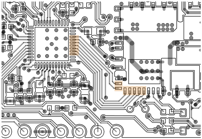
shows the highlighted pins, which are internally routed according to the PWM U, V, W, high and low side signal input sequence of the IPM and the kill output going to the MCU. Any GPIO pin can be used as kill input for multiple TCPWM counters. The internal signal routing flexibility simplifies the PCB layout using the PSOC™ Control C3 MCU especially for two-layer PCB designs.
Signal routing
If only a two-layer PCB is used, one layer can be used for routing traces vertically while the other layer can be used to route traces horizontally. This can minimize crosstalk and also minimizes the possibility of creating discontinuity in the GND planes.
For four-layer or six-layer PCBs, use dedicated layers for signal routing (analog and high-speed digital on the same layer as the MCU as far as possible and auxiliary signals on other layers).
Analog signals
Analog signals are more prone to noise compared to digital signals. The impact of noise may manifest as unwanted variations in the converted ADC value or lead to false triggering in case of comparator inputs. Routing for critical analog signals should be prioritized. Try to route the analog signals away from high speed and high current switching signal.
Discrete RC filters
RC low-pass filters can be added to the ADC inputs to reduce RF noise. The RC time constant should be selected as per the expected signal bandwidth. The RC should be placed close to the analog input pin with the capacitor placed closer to the pin followed by the resistor. The signal trace is connected to the far end of the resistor (away from the MCU pin). The closer resistor pad (to the MCU pin) is connected to the capacitor pad and then the capacitor pad trace is connected to the analog input pin.
Schematic checklist
The following checklists help ensure that important design elements are not overlooked. The answer to each of the entries should be Yes (Y), No (N), or Not Applicable (NA). This checklist does not guarantee 100% coverage of all use cases/scenarios. However, it can be used as a starting point and customized/enhanced further as per individual design requirements.
Power checklist
Item | Y/N/NA | Remark |
|---|---|---|
Are the power pin connections made in accordance with Power pin connections? | ||
Are decoupling capacitors placed as per recommended values on VDDD, VDDIO and VDDA? | ||
Are the voltages (including ripples) at the VDDD and VDDA pins in the range of 1.71 V to 3.6 V? | ||
Is the VCCD pin connected to a 4.7 μF capacitor? | ||
Is the VBACKUP pin connected to an appropriate supply (VDDD or the 1.4 V to 3.6 V source)? |
Clocking checklist
Item | Y/N/NA | Remarks |
|---|---|---|
Is the external clock connected to the EXT_CLK pin? | ||
Is the external clock’s frequency less than or equal to 80 MHz (including tolerance)? | ||
Is the external crystal connected to the ECO pins for ECO operation (4 MHz to 35 MHz)? Are the ECO load capacitors connected? | ||
Is the 32.768 kHz crystal connected to the WCO for RTC operation? Are the WCO load capacitors connected? |
Reset checklist
Item | Y/N/NA | Remarks |
|---|---|---|
Is the reset pin connection made in accordance with XRES? | ||
Is Reset button connected between XRES and GND? |
Programming and debugging checklist
Item | Y/N/NA | Remarks |
|---|---|---|
Are SWD signals connected as described in SWD? | ||
Are JTAG signals connected as described in JTAG? | ||
Are ETM signals connected as described in Embedded Trace Macrocell (ETM)? | ||
Are DFU select and communication pins connected as described in Device Firmware Update (DFU)? |
GPIO pins checklist
Item | Y/N/NA | Remarks |
|---|---|---|
Is the assignment of your GPIO pins done in the sequence described in I/O pin selection? |
SCB and CAN checklist
Item | Y/N/NA | Remarks |
|---|---|---|
Is the assignment of the SCB’s fixed pins in accordance with the device datasheet for the following SCBs: | ||
SCB0? | ||
SCB1? | ||
SCB2? | ||
SCB3? | ||
SCB4? | ||
SCB5? | ||
Is the assignment of the CAN fixed pins in accordance with the device datasheet? |
ADC checklist
Item | Y/N/NA | Remarks |
|---|---|---|
Is the VAREF_EXT pin connected externally to VDDA or a dedicated reference voltage between 1.7 V to VDDA? | ||
Is the VAREF_EXT pin connected to a 2.2 μF capacitor? | ||
Is the connection to ADC analog input pins done per the device datasheet specified pinout? |
Summary
The
PSOC™ Control C3
provides a flexible solution for designing digital and analog applications including, but not limited to, real-time control applications. This application note documents the considerations that need to be considered when building a hardware system around the
PSOC™ Control C3
.
References
For more PSOC™ Control C3 MCU-related documents, see the
PSOC™ Control C3 MCU
,
PSOC™ Control C3P
, and
PSOC™ Control C3M
product webpages.
Architecture reference manual
Device datasheet
Datasheet PSOC™ Control C3- PSC3P5xD, PSC3M5xD
Datasheet PSOC™ Control C3- PSC3P2xD, PSC3M3xD
Revision history
Document revision | Date | Description of changes |
|---|---|---|
** | 2024-05-30 | Initial release |
*A | 2024-12-17 | Updated the following sections:
Added Device Firmware Update (DFU) section |
1
Maximum clock frequency after the corresponding clock source (DPLL/FLL + dividers). All internal tolerances and affects are covered by these frequencies.
2
The minimum permitted clock frequency of HPPASS is 60 MHz.