AN240040 How to use trigger multiplexer in PSOC™ Control C3 MCU
About this document
Scope and purpose
This application note introduces the trigger multiplexer features of the
PSOC™ Control C3
MCU and discusses how to use these peripheral functions in actual applications.
Intended audience
This document is intended for anyone who uses the trigger multiplexer of the
PSOC™ Control C3
MCUs.
Trigger multiplexer introduction
Every peripheral in the PSOC™ Control C3 device is interconnected using trigger signals. Trigger signals are means by which peripherals inform the occurrence of an event or transition to a different state. Trigger signals are used to initiate an action in other peripherals. For example, the TCPWM output signal can be routed to another two TCPWM as a trigger in the signal via the trigger multiplexer group trigger function. The TCPWM output signal can also be routed to the HPPASS SAR ADC as a trigger signal via the trigger multiplexer one-to-one trigger function. Trigger multiplexers are simple multiplexers that are designed to route these trigger signals from the source peripherals to the desired destinations.
In this application note, you will learn how to set up trigger routes from the source peripherals to the desired destinations. To know more about the functionality and terminology used in this application note, see the “Trigger multiplexer (Trigger MUX)” chapter of the PSOC™ Control C3 architecture reference manual.
Trigger component overview
The trigger component triggers signals. The trigger input signals (for a multiplexer) are typically peripheral output signals. The trigger output signals (of a multiplexer) are typically peripheral input signals. In general, a trigger input signal indicates the completion of a peripheral action or a peripheral event. In general, a trigger output signal initiates a peripheral action.
The trigger multiplexer has two group types:
Multiplexer-based group type (multiplexer trigger)
This type connects a peripheral input trigger to multiple peripheral output triggers. The selection is under software control: PERI_TR_GR_TR_CTL.TR_SEL
One-to-one-based group type (one-to-one trigger)
This type connects a peripheral input trigger to a specific output trigger
The trigger component provides 15 multiplexer-based trigger groups and 3 one-to-one trigger groups. Figure 1 shows the trigger component block diagram.
Figure 1.
Trigger component block diagram
The trigger component has the following input and output signals:
TRIG_IN_MUX_x is the input trigger of the multiplexer trigger
TRIG_IN_1TO1_x is the input trigger of the one-to-one trigger
TRIG_OUT_MUX_x is the output trigger of the multiplexer trigger
TRIG_OUT_1TO1_x is the output trigger of the one-to-one trigger
SW control is provided for trigger activation. This control allows for the activation of a specific trigger. For level-sensitive triggers, the trigger activation is completely under SW control. For edge-sensitive triggers, the trigger activation is two high/’1’ cycles on CLK_PERI.
Trigger propagation can be blocked in debug mode (typically when a CPU is halted). This allows it to isolate the trigger consumer peripheral from getting input triggers during a debug halt. The debug mode is indicated by the level trigger input x_DEBUG_FREEZE_TR_IN1, which is connected to a CPUSS CTI trigger output.
The suffix “x” represents the name of the peripheral block. Table 1 shows the output triggers and the input triggers of a multiplexer trigger that can be routed to each other and the availability of routing in the PSOC™ Control C3 device series. However, some combinations cannot be routed to some unit and channel numbers. For details on the units and channels of each peripheral, see the “Trigger multiplexer (Trigger MUX)” chapter of the PSOC™ Control C3 architecture reference manual.
TRIG_IN_MUX_x | Trigger multiplexer | TRIG_OUT_MUX_x |
|---|---|---|
IOSS [0:49] | MOTIF Trigger | TCPWM.motif_in[0:7] |
HPPASS tr_level_out[0:7] | ||
8x16-bit TCPWM [GP1 counter out0, out1] | ||
HPPASS [all] | TCPWM0 Trigger | TCPWM.tr_all[0:3] |
LPCOMP [comp0, comp1] | ||
SCB [all] | TCPWM1 Trigger | TCPWM.tr_all [4:15] |
CPUSS.tr_fault [0] | ||
DW0, DW1 [all] | ||
CANFD.tmp_rpt_out | ||
TCPWM1 [out1 only] | ||
IOSS [0:49] | ||
TCPWM.tr_motif_out[0:7] | ||
IOSS [0:49] | TCPWM2 Trigger | TCPWM.tr_one[trigger 3 (20 x counter)] |
TCPWM1 [out0 only] | TCPWM3 Trigger | TCPWM.tr_one[trigger 4 (20 x counter)] |
TCPWM1 [out1 only] | HPPASS Trigger | HPPASS.tr_muxed_in[all] |
IOSS [0:49] | ||
TCPWM.tr_motif_out[0:7] | ||
TCPWM [all out0] | PDMA0 | DW0 -16 channels |
IOSS [0:49] | ||
SCB [6x3] (all) | ||
HPPASS [all] | ||
LPCOMP [comp0, comp1] | ||
CORDIC.done_mxcordic | ||
CRYPTOLITE.tr_trng_bitstream | ||
CANFD [all] | ||
CPUSS.tr_fault [0] | ||
DEBUG600.CTI_out [0:1] | ||
Same "in" as PDMA0 | PDMA1 | DW1 -16 channels |
DW0 [0-3] | HSIOM0 Trigger | IOSS.peri_tr_io_input_in[0:49] |
DW0 [all] | ||
DW1 [all] | ||
CPUSS. CTI_out [0:1] | ||
SCB [all] | ||
CANFD.tmp_rpt_out | ||
TCPWM [all out1] | ||
TCPWM tr_line [0:19] | ||
TCPWM.tr_motif_out[0:7] | ||
HPPASS [all] | ||
LPCOMP [comp0, comp1] | ||
CORDIC.done_mxcordic | ||
CRYPTOLITE.tr_trng_bitstream | ||
IOSS.peri_tr_io_input_in[0:49] | ||
TCPWM [line][0:3] | HSIOM1 Trigger | IOSS.peri_tr_io_input_in[50:57] |
TCPWM [line_compl ][0:3] | ||
TCPWM [line][256:259] | HSIOM2 Trigger | IOSS.peri_tr_io_input_in[58:65] |
TCPWM [line_compl] [256:259] | ||
TCPWM [line][512:515] | HSIOM3 Trigger | IOSS.peri_tr_io_input_in[66:73] |
TCPWM [line_compl] [512:515] | ||
DW0 [all] | CPUSS_CTI | CPUSS.CTI_in[0:1] |
DW1 [all] | SRSS.debug_freeze_mcwdt | |
DEBUG600.CTI_out [0:1] | ||
CPUSS.tr_fault [0] | ||
TCPWM [all out0, out1] | ||
IOSS [all pads] | ||
SCB [all] | ||
CANFD.tmp_rpt_out [0:1] | ||
HPPASS [all] | ||
LPCOMP [comp0, comp1] | ||
CORDIC.done_mxcordic | ||
CORDIC.start_mxcordic | ||
TCPWM.tr_motif_out[0:7] | ||
DEBUG600.CTI_out [0:1] | PREI_FREEZE | TCPWM.debug_freeze |
CPUSS.tr_fault [0] | ||
CANFD.tmp_rpt_out[0:1] | CANTT | CANFD.evt_swt_in[0:1] |
In a one-to-one group trigger, one input trigger is directly connected to a specific output trigger. For the routing of the one-to-one trigger, see the “Trigger multiplexer (Trigger MUX)” chapter of the PSOC™ Control C3 architecture reference manual.
Multiplexer trigger
For a multiplexer trigger, an input trigger (TRIG_IN_MUX_x) is selected for each output trigger (TRIG_OUT_MUX_x). Figure 2 shows the multiplexer trigger block diagram.
Note: All output triggers in a group share the same input triggers.
Figure 2.
Multiplexer trigger
One of the multiple output signals from the source peripheral is selected. For a specific output trigger in the trigger group, the input trigger can be specified via the PERI[i]_TR_GR[x]_TR_CTL[y] register. Here, ‘i’ is the peri group number, ‘x’ is the trigger group number, and ‘y’ is the output trigger line number from the multiplexer. The input trigger number can be specified by PERI[i]_TR_GR[x]_TR_CTL[y].TR_SEL=j. This section describes an example of group triggers. See the register bit details in
PSOC™ Control C3
MCU registers.
This example demonstrates that the trigger of the 16-bit TCPWM0 Group1 Counter6 starts upon receiving the 16-bit TCPWM0 Group1 Counter5 OUT1 signal. This trigger routing is included in multiplexer group 10. This example is extracted from the
PSOC™ Control C3
architecture reference manual, which provides the trigger group, input trigger, and output trigger.
Table 2
and
Table 3
show the trigger inputs and trigger outputs of multiplexer group 10.
Trigger MUX input | Trigger source label | Description |
|---|---|---|
0 | ZERO | – |
1:16 | PDMA0_TR_OUT[0:15] | P-DMA0 tr_out |
17:32 | PDMA1_TR_OUT[0:15] | P-DMA1 tr_out |
33 | TCPWM0_GRP0_OUT1_[0] | 32-bit TCPWM counters to PDMA1 |
34 | TCPWM0_GRP0_OUT1_[1] | – |
35 | TCPWM0_GRP0_OUT1_[2] | – |
36 | TCPWM0_GRP0_OUT1_[3] | – |
37 | TCPWM0_GRP1_OUT1_[0] | 16-bit TCPWM counters to PDMA1 |
38 | TCPWM0_GRP1_OUT1_[1] | – |
39 | TCPWM0_GRP1_OUT1_[2] | – |
40 | TCPWM0_GRP1_OUT1_[3] | – |
41 | TCPWM0_GRP1_OUT1_[4] | – |
42 | TCPWM0_GRP1_OUT1_[5] | – |
43 | TCPWM0_GRP1_OUT1_[6] | – |
44 | TCPWM0_GRP1_OUT1_[7] | – |
Trigger MUX output | Trigger destination label | Description |
|---|---|---|
0:11 | TCPWM0_TR_IN [4:15] | Triggers to TCPWM0 |
Figure 3.
Trigger routing between two 16-bit TCPWMs
The following explains how to connect TCPWM[0].tr_out[261] and TCPWM[0].tr_all_cnt_in[13].
Configuration register selection
Peripheral group is 10 (i=10)
Multiplexer group is 10 (x=10)
Output trigger TRIG_OUT_MUX_10_TCPWM0_TR_IN[13] (y=9)
Therefore, the register is specified as PERI10_TR_GR10_TR_CTL9
Input trigger selection
Input trigger TRIG_IN_MUX_10_TCPWM0_GRP1_OUT1[5] (j=42)
The configuration will be PERI10_TR_GR10_TR_CTL9.TR_SEL = 42
One-to-one trigger
For a one-to-one trigger, an input trigger (TRIG_IN_1TO1_x) is connected to the output trigger (TRIG_OUT_1TO1_x). A one-to-one group has the AND gate functionality to disable an input trigger.
Figure 4
shows the one-to-one trigger block diagram.
Figure 4.
1-to-1 trigger block diagram
A one-to-one group trigger can be specified by the PERI[i]_TR_GR[x]_TR_CTL[y] register. Here, ‘i’ is the peri group, ‘x’ is the trigger group, and ‘y’ is the output trigger line number from the multiplexer.
PERI[i]_TR_GR[x]_TR_CTL[y]. TR_SEL is used to control the enabling/disabling of the input trigger. If set to ‘1’, the input trigger is enabled. If set to ‘0’, the input trigger is disabled and sets the signal level to a constant ‘0’.
This section describes an example of a one-to-one trigger.
This is an example of how to trigger ADC group 0 channel 7 by a 16-bit TCPWM0 Group1 Counter5 OUT1 signal. This trigger routing is included in one-to-one trigger group 2. The example is based on Table 4 extracted from the PSOC™ Control C3 architecture reference manual that provides trigger input and trigger output for one-to-one trigger group 2.
Trigger MUX input | Trigger Mux label | Description |
|---|---|---|
0 | TCPWM0_GRP0_CNT2_OUT1_TO_HPPASS_TR_IN[0] | TCPWM Group[0], Counter[2], OUT1 to HPPASS |
1 | TCPWM0_GRP0_CNT3_OUT1_TO_HPPASS_TR_IN[1] | TCPWM Group[0], Counter[3], OUT1 to HPPASS |
2 | TCPWM0_GRP1_CNT5_OUT1_TO_HPPASS_TR_IN[2] | TCPWM Group[1], Counter[5], OUT1 to HPPASS |
3 | TCPWM0_GRP1_CNT6_OUT1_TO_HPPASS_TR_IN[3] | TCPWM Group[1], Counter[6], OUT1 to HPPASS |
4 | TCPWM0_GRP1_CNT7_OUT1_TO_HPPASS_TR_IN[4] | TCPWM Group[1], Counter[7], OUT1 to HPPASS |
5 | TCPWM0_GRP2_CNT5_OUT1_TO_HPPASS_TR_IN[5] | TCPWM Group[2], Counter[5], OUT1 to HPPASS |
6 | TCPWM0_GRP2_CNT6_OUT1_TO_HPPASS_TR_IN[6] | TCPWM Group[2], Counter[6], OUT1 to HPPASS |
7 | TCPWM0_GRP2_CNT7_OUT1_TO_HPPASS_TR_IN[7] | TCPWM Group[2], Counter[7], OUT1 to HPPASS |
Figure 5.
One-to-one trigger routing between TCPWM0 and HPPASS
In a one-to-one group trigger, one input trigger is directly connected to a specific output trigger. Thus, specifying only the input trigger number is sufficient to indicate its output trigger.
The following explains how to connect TCPWM[0].tr_out[261] and HPPASS.tr_b_in[2].
Configuration register selection
Peripheral group is 10 (i=10)
Multiplexer one-to-one group is 2 (x=2)
Input trigger TCPWM0_GRP1_CNT5_OUT1, which directly connects to output trigger HPPASS_TR_IN[2] (y=2).Therefore, the register is specified as PERI10_TR_1TO1_GR2_TR_CTL2
Input trigger configuration
Typically, the input trigger of a one-to-one trigger is enabled.
The configuration will be PERI10_TR_1TO1_GR2_TR_CTL2.TR_SEL = 1
Trigger multiplexer control
The input trigger and output trigger for the multiplexer group and the one-to-one group trigger are controlled by RREI[i]_TR_GRP[x]_TR_CTL[y ] and PERI[i]_TR_1TO1_GRP[x]_TR_CTL[y] registers. This section will show registers for each bit in detail. For more related registers, refer to PSOC™ Control C3 MCU registers.
RREI[i]_TR_GRP[x]_TR_CTL[y ] Bits | Name | Description |
|---|---|---|
0:6 | TR_SEL | Specifies the input trigger. Note that input trigger 0 (default value) is typically connected to a constant signal level of '0', and as a result, this will not cause HW activation of the output trigger. Default Value: 0 |
8 | TR_INV | Specifies if the output trigger is inverted. ‘0’: Not inverted ‘1’: Inverted |
9 | TR_EDGE | Specifies if the (inverted) output trigger is treated as a level-sensitive or edge-sensitive trigger. ‘0’: Level-sensitive ‘1’: Edge-sensitive trigger |
12 | DEBUG_FREEZE | Specifies if the output trigger is blocked in debug mode. ‘0’: enable output trigger generation ‘1’: Block output trigger generation |
RREI[i]_TR_1TO1_GRP[x]_TR_CTL[y ] Bits | Name | Description |
|---|---|---|
0:6 | TR_SEL | Specifies input trigger. ‘0’: Constant signal level ‘0’ ‘1’: Input trigger |
8 | TR_INV | Specifies if the output trigger is inverted. ‘0’: Not inverted ‘1’: Inverted |
9 | TR_EDGE | Specifies if the (inverted) output trigger is treated as a level-sensitive or edge-sensitive trigger. ‘0’: Level-sensitive ‘1’: Edge-sensitive trigger |
12 | DEBUG_FREEZE | Specifies if the output trigger is blocked in debug mode. ‘0’: enable output trigger generation ‘1’: Block output trigger generation |
Applications
This section shows how to use the trigger multiplexer signal routing function in ModusToolbox™. This section also describes the following use cases for the multiplexer group trigger and the one-to-one group trigger:
TCPWM trigger two TCPWMs
TCPWM trigger SAR ADC
Three TCPWMs trigger SAR ADC via SMART I/O
TCPWM trigger two TCPWMs
This section explains how to use one TCPWM output signal to trigger another two TCPWMs to start working.
Use case description
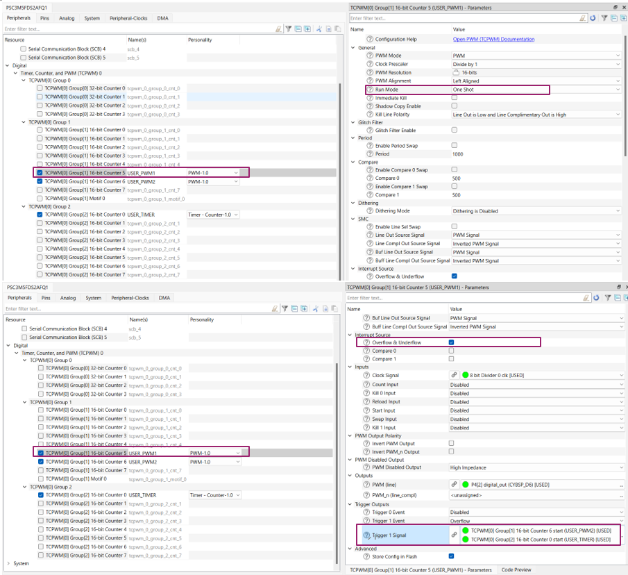
Figure 6 shows an example for TCPWM0 Group1 Counter5 to generate out trigger signal. Connect this out trigger to TCPWM0 Group1 Counter6 and TCPWM0 Group2 Counter0 by trigger multiplexer group 10. Configure the TCPWM0 Group1 Counter5 to USER_PWM 1, set the run mode to one-shot mode, enable the Overflow & Underflow interrupt, set the output trigger 1 event to overflow, and select the output trigger destination to start TCPWM0 Group1 Counter6 (USER_PWM2) and TCPWM0 Group2 Counter0 (USER_Timer). For more details on the TCPWM component, see the “Timer, counter, and pulse-width modulator (TCPWM)” chapter of the
PSOC™ Control C3
architecture reference manual. For trigger input and trigger output connection details, see the “Trigger multiplexer (Trigger MUX)” chapter of the
PSOC™ Control C3
architecture reference manual.
Figure 6.
Example of trigger multiplexer group trigger in PSOC™ C3
Figure 7.
Example of multiplexer group trigger flow in PSOC™ C3
Device configuration design
to
Figure 10
show the USER_PWM1, USER_PWM2, and USER_TIMER peripheral parameter configurations in the ModusToolbox™ IDE device configurator tool.
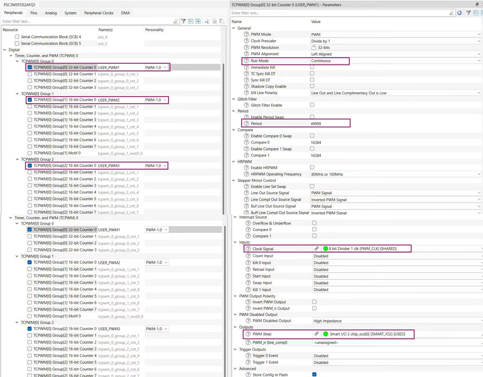
shows the USER_PWM1 set PWM mode with one shot run mode, enable the PWM Overflow & Underflow interrupt source, PWM signal output to P4[2], and the user can observe the PWM waveform via P4[2], enable the overflow trigger out event, and routing to USER_PWM2 and USER_Timer.
Figure 8.
USER_PWM1 configuration
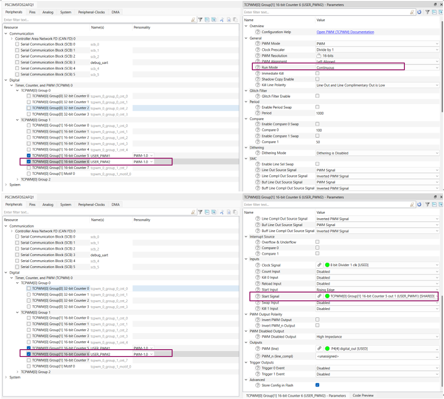
shows the USER_PWM2 set PWM mode with continue run mode; the start signal is connected to USER_PWM1, and the PWM signal output to P4[4]. The user can observe the PWM waveform via P4[4]. Once USER_PWM1 generates the overflow output event, it will start the USER_PWM2 to work.
Figure 9.
USER_PWM2 configuration
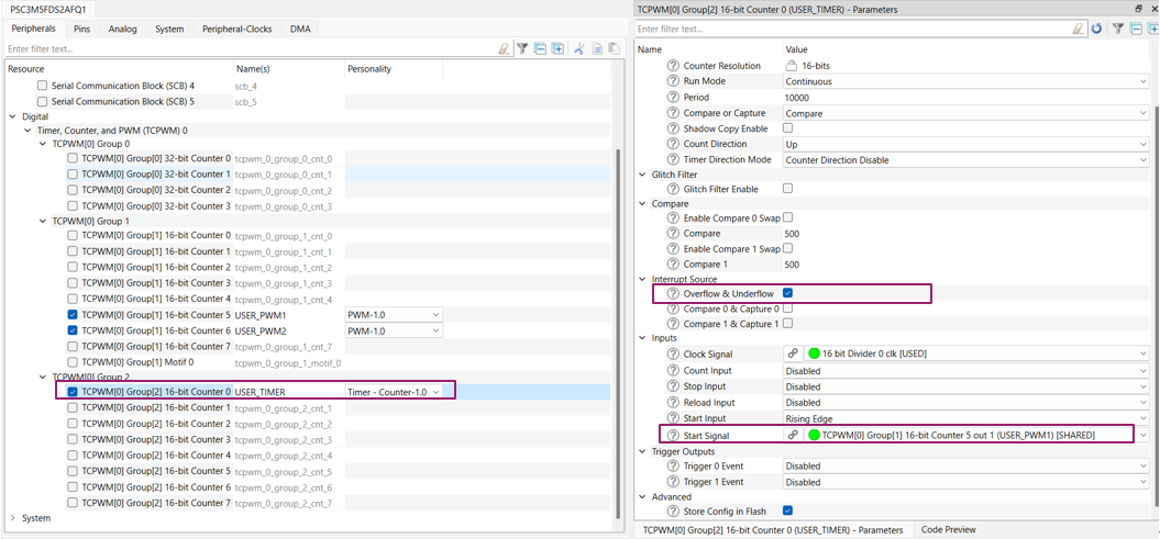
shows USER_Timer set to Timer mode, enabling the Overflow & Underflow interrupt source, and the start signal being connected to USER_PWM1. Once USER_PWM1 generates the overflow output event, it will start the USER_Timer to work.
Figure 10.
USER_Timer configuration
Code snippet
Code listing 1 shows the source codes of this example.
Code listing 1
int main(void)
{
cy_rslt_t result;

/* Initialize the device and board peripherals */
result = cybsp_init();
/* Board init failed. Stop program execution */
if (result != CY_RSLT_SUCCESS)
{
CY_ASSERT(0);
}

result = cy_retarget_io_init_fc(CYBSP_DEBUG_UART_TX, CYBSP_DEBUG_UART_RX,
    CYBSP_DEBUG_UART_CTS,CYBSP_DEBUG_UART_RTS,CY_RETARGET_IO_BAUDRATE);

/* retarget-io init failed. Stop program execution */
if (result != CY_RSLT_SUCCESS)
{
CY_ASSERT(0);
}

/* Initialize PWM 1 using the config structure generated using device configurator*/
if (CY_TCPWM_SUCCESS != Cy_TCPWM_PWM_Init(USER_PWM1_HW, USER_PWM1_NUM, &USER_PWM1_config))
{
CY_ASSERT(0);
}
/* Configure user PWM1 interrupt */
Cy_SysInt_Init(&user_pwm1_intr_config, user_pwm1_intr_handler);
NVIC_EnableIRQ(user_pwm1_intr_config.intrSrc);
/* Enable the initialized PWM1 */
Cy_TCPWM_PWM_Enable(USER_PWM1_HW, USER_PWM1_NUM);

/* Initialize PWM 2 using the config structure generated using device configurator*/
if (CY_TCPWM_SUCCESS != Cy_TCPWM_PWM_Init(USER_PWM2_HW, USER_PWM2_NUM, &USER_PWM2_config))
{
CY_ASSERT(0);
}

/* Initialize timer using the config structure generated using device configurator*/
if (CY_TCPWM_SUCCESS != Cy_TCPWM_Counter_Init(USER_TIMER_HW, USER_TIMER_NUM, &USER_TIMER_config))
{
CY_ASSERT(0);
}
/* Configure user timer interrupt */
Cy_SysInt_Init(&user_timer_intr_config, user_timer_intr_handler);
NVIC_EnableIRQ(user_timer_intr_config.intrSrc);

user_timer_is_running = false;
user_timer_int_flag = false;
user_timer_int_cnt = 0;

/* Enable global interrupts */
__enable_irq();

for (;;)
{
/* Check if 'Enter' key was pressed */
if (cyhal_uart_getc(&cy_retarget_io_uart_obj, &uart_read_value, 1) == CY_RSLT_SUCCESS)
{
    if ((uart_read_value == '\r') && (!user_timer_is_running))
    {
        user_timer_int_cnt = 0;
        user_timer_is_running = true;
        Cy_GPIO_Write(CYBSP_USER_LED_PORT, CYBSP_USER_LED_PIN, CYBSP_LED_STATE_ON);
        /* Enable the initialized PWM2 */
        Cy_TCPWM_PWM_Enable(USER_PWM2_HW, USER_PWM2_NUM);
        /* Enable the initialized TIMER */
        Cy_TCPWM_Counter_Enable(USER_TIMER_HW, USER_TIMER_NUM);
        /* Start PWM1 */
        printf("\r\nStart user PWM1\r\n");
        Cy_TCPWM_TriggerStart_Single(USER_PWM1_HW, USER_PWM1_NUM);
    }
}
/* Check the interrupt flag of user timer */
if(user_timer_int_flag)
{
    user_timer_int_flag = false;
    printf("User timer terminal count (TC) interrupt, toggle USER_LED\r\n");
    /* Toggle user LED */
    Cy_GPIO_Inv(CYBSP_USER_LED_PORT, CYBSP_USER_LED_PIN);
    /* Check the interrupt times of user timer */
    user_timer_int_cnt++;
    if(USER_TIMER_INT_MAX_NUM <= user_timer_int_cnt)
    {
        user_timer_is_running = false;
        Cy_GPIO_Write(CYBSP_USER_LED_PORT, CYBSP_USER_LED_PIN, CYBSP_LED_STATE_OFF);
        /* Disable PWM2 and timer */
        printf("Disable user PWM2 and timer\r\n");
        Cy_TCPWM_PWM_Disable(USER_PWM2_HW, USER_PWM2_NUM);
        Cy_TCPWM_Counter_Disable(USER_TIMER_HW, USER_TIMER_NUM);
    }
}
}
}
TCPWM trigger SAR ADC
This section explains how to use one TCPWM output signal to trigger the SAR ADC to start working.
Use case description
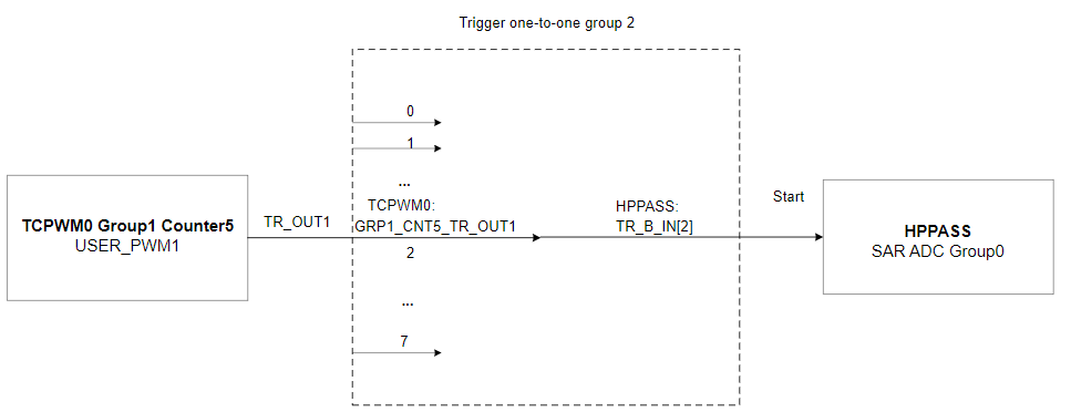
shows an example for TCPWM0 Group1 Counter5 (USER_PWM1) to generate out trigger signal. Connect this out trigger to HPPASS SAR ADC group 0 by trigger one-to-one group 2. Configure the USER_PWM 1, set its run mode to one-shot mode and enable Overflow & Underflow interrupt, set the output trigger 1 event to overflow, and select the output trigger destination to HPPASS input trigger 2. For more details on the HPPASS component, see the “High-performance programmable analog subsystem (HPPASS)” chapter of the
PSOC™ Control C3
architecture reference manual. For trigger input and trigger output connection details, see the
One-to-one trigger
section.
Figure 11.
Example of one-to-one trigger in PSOC™ C3
Device configuration design
and
Figure 13
show the USER_PWM1 and HPPASS peripheral parameter configurations in the ModusToolbox™ IDE device configurator tool.
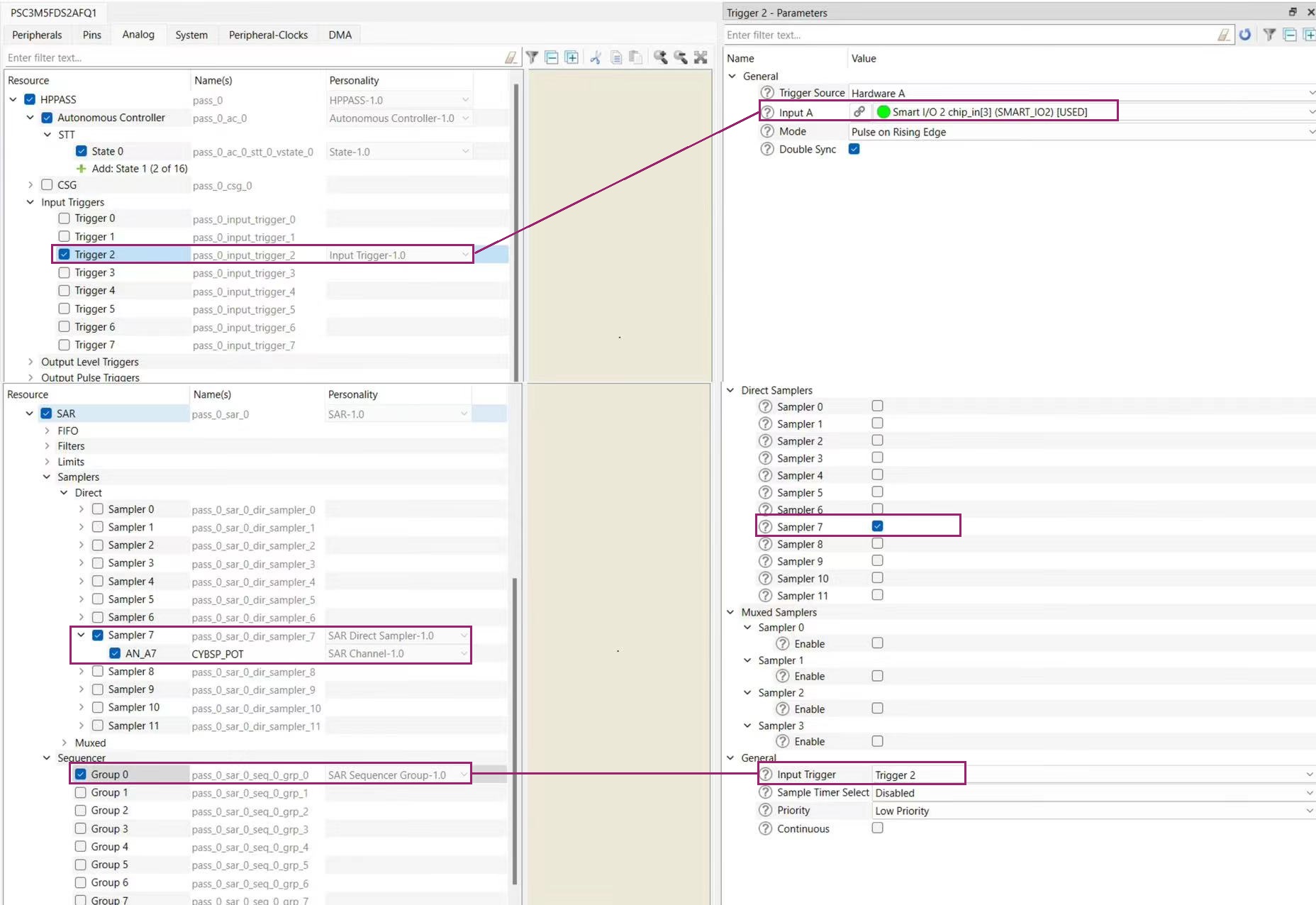
shows the USER_PWM1 set PWM mode with one shot run mode, enable the PWM Overflow & Underflow interrupt source, PWM signal output to P4[2], and the user can observe the PWM waveform via P4[2], enable the overflow trigger out event, and route to HPPASS input trigger 2.
Figure 12.
USER_PWM1 configuration for HPPASS
shows how to configure HPPASS and ADC channel AN_A7, enable ADC sampler 7 in ADC group 0, select HPPASS input trigger 2 for ADC group 0, and set HPPASS input trigger 2 to hardware B (one-to-one trigger). This one-to-one trigger is connected to the USER_PWM1 output trigger.
Figure 13.
HPPASS configuration
Code snippet
shows the source codes of this example.
Code listing 2
int main(void)
{
cy_rslt_t result;

/* Initialize the device and board peripherals */
result = cybsp_init();
/* Board init failed. Stop program execution */
if (result != CY_RSLT_SUCCESS)
{
CY_ASSERT(0);
}

result = cy_retarget_io_init_fc(CYBSP_DEBUG_UART_TX, CYBSP_DEBUG_UART_RX,
    CYBSP_DEBUG_UART_CTS,CYBSP_DEBUG_UART_RTS,CY_RETARGET_IO_BAUDRATE);

/* retarget-io init failed. Stop program execution */
if (result != CY_RSLT_SUCCESS)
{
CY_ASSERT(0);
}

/* Configure ADC group 0 done interrupt */
Cy_HPPASS_SAR_Result_SetInterruptMask(CY_HPPASS_INTR_SAR_RESULT_GROUP_0);
Cy_SysInt_Init(&adc_group0_done_intr_config, adc_group0_done_intr_handler);
NVIC_EnableIRQ(adc_group0_done_intr_config.intrSrc);

/* Start the HPPASS autonomous controller (AC) from state 0 */
if(CY_HPPASS_SUCCESS != Cy_HPPASS_AC_Start(0U, 10000u))
{
CY_ASSERT(0);
}

/* Enable global interrupts */
__enable_irq();

for (;;)
{
/* Check if 'Enter' key was pressed */
if (cyhal_uart_getc(&cy_retarget_io_uart_obj, &uart_read_value, 1) == CY_RSLT_SUCCESS)
{
    if ((uart_read_value == '\r'))
    {
        /* Start PWM1 */
        printf("\r\nStart user PWM1\r\n");
        Cy_TCPWM_TriggerStart_Single(USER_PWM1_HW, USER_PWM1_NUM);
    }
}

/* Check whether the ADC conversion is complete */
if(adc_group0_int_flag)
{
    adc_group0_int_flag = false;
    /* Convert the ADC result to voltage */
    float32_t volts = Cy_HPPASS_SAR_CountsTo_Volts(CY_HPPASS_SAR_CHAN_7_IDX, 3300, adc_result_buf);
    printf("ADC AN_A7 channel result = 0x%x, voltage = %.4fV\r\n", adc_result_buf, volts);
}

}
}
Three TCPWMs trigger SAR ADC via SMART I/O
This section explains how to combine the Trigger Multiplexer and SMART I/O function to trigger activation of the SAR ADC.
Use case description
illustrates an example in which three TCPWM modules route three PWM output line signals to the SMART I/O module. These three signals are then combined via SMART I/O LUT3 to produce a single signal output that triggers the start of the SAR ADC.
TCPWM0 Group 0 Counter 0 (USER_PWM1), TCPWM0 Group 1 Counter 0 (
USER_PWM2
), and TCPWM0 Group 2
Counter 0 (
USER_PWM3) operate at the same clock
frequency (1 MHz) and are configured in PWM continuous mode. Each TCPWM module's PWM
output line signals (TR_LINE0,TR_LINE256, and TR_LINE512) are enabled and routed to the SMART I/O
module as LUT3 inputs. The GPIO PORT2 SMART I/O function is enabled, and its output
signal is configured to route to the HPPASS input trigger 2 to initiate SAR ADC
operation. SAR ADC samples the external 3.3 V voltage and outputs the voltage value to
the UART terminal.
For more details on the HPPASS and SMART I/O components, see the High-performance programmable analog subsystem (HPPASS) and Programmer digital (Smart I/O) chapters of the PSOC™ Control C3 architecture reference manual.
Figure 14.
Three TCPWMs trigger SAR ADC via SMART I/O diagram
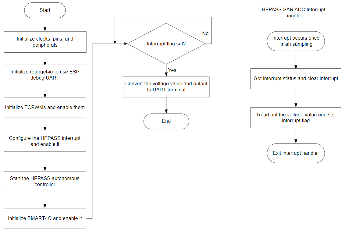
shows the implementation flow for the use case.
Figure 15.
Three TCPWMs trigger SAR ADC via SMART I/O flow
Device configuration design
shows the parameter configurations for the
USER_PWM1
,
USER_PWM2
, and
USER_PWM3
peripherals in the ModusToolbox™ IDE device configurator tool. The TCPWM operates at a clock frequency of 1 MHz in continuous mode with a counter period of 50000. The PWM output lines are enabled and routed to the SMART I/O.
TCPWM0 Group0 Counter0 (
USER_PWM1) PWM output line routing to GPIO PORT2 SMART I/O chip 0 inputTCPWM0 Group1 Counter0 (
USER_PWM2) PWM output line routing to GPIO PORT2 SMART I/O chip 1 inputTCPWM0 Group2 Counter0 (
USER_PWM3) PWM output line routing to GPIO PORT2 SMART I/O chip 2 input
Figure 16.
USER TCPWMs configuration
shows the parameter configuration for the HPPASS module.
The HPPASS autonomous controller (AC) is enabled with default settings, and the AC state0 is added with default settings. Additionally, the SAR is enabled, and the reference voltage is set to 3300 mV from an External (VAREF_EXT) source. Group0 is enabled, and the ADC AN_A7 sample channel and Trigger 2 is set as the input trigger.
Figure 17.
HPPASS configuration
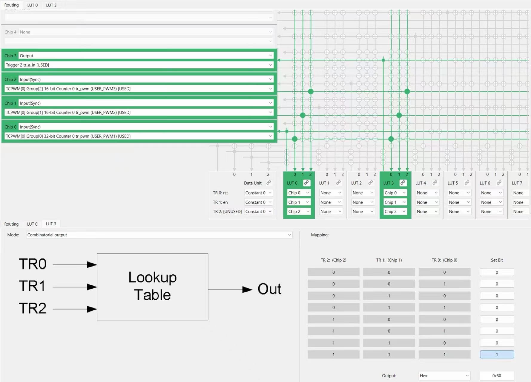
shows the parameter configuration for the SMART I/O module. ModusToolbox™ IDE features a standalone SMART I/O configuration tool. For instructions on how to open and use it, refer to the IDE help documents.
Enable SMART I/O 2 Port and set the peripheral clock divider (ACTIVE) as the clock. Enable the 8-bit divider 0 clk
Configure the SMART I/O input signals from chip0, chip1, and chip2. Enable LUT0 and set the PWM output lines of TCPWM0 Group0 Counter0 (
USER_PWM1), TCPWM0 Group1 Counter0 (USER_PWM2), and TCPWM0 Group2 Counter0 (USER_PWM3) to route to chip0, chip1, and chip2Enable LUT3 and set chip0, chip1, and chip2 as inputs. Configure chip3 as the SMART I/O output signal and connect chip3 to HPPASS trigger 2 input. Configure the LUT3 truth table, ensuring that the signal output is without invert
Figure 18.
SMART I/O configuration
Code snippet
Code Listing 3 shows the source code snippet of TCPWMs trigger SAR ADC via SMART I/O.
Code listing 3
/* The interrupt configuration structure of ADC group 0 done */
cy_stc_sysint_t adc_group0_done_intr_config =
{
.intrSrc = pass_interrupt_sar_entry_done_0_IRQn,
.intrPriority = 0U,
};

/* ADC channel result buffer */
uint16_t adc_result_buf = 0;

/* ADC group 0 interrupt flag */
volatile bool adc_group0_int_flag = false;

/* ADC group 0 done interrupt handler */
void adc_group0_done_intr_handler(void);

int main(void)
{
cy_rslt_t result;
/* Initialize the device and board peripherals */
result = cybsp_init();

/* Board init failed. Stop program execution */
if (result != CY_RSLT_SUCCESS)
{
CY_ASSERT(0);
}

/* Initialize retarget-io to use the debug UART port */
result = cy_retarget_io_init_fc(CYBSP_DEBUG_UART_TX,
                            CYBSP_DEBUG_UART_RX,
                            CYBSP_DEBUG_UART_CTS,
                            CYBSP_DEBUG_UART_RTS,
                            CY_RETARGET_IO_BAUDRATE);

if (result != CY_RSLT_SUCCESS)
{
 CY_ASSERT(0);
}

/* \x1b[2J\x1b[;H - ANSI ESC sequence for clear screen */
printf("\x1b[2J\x1b[;H");
printf("***********************************************************\r\n");
printf("Use case: TriggerMux and Smart I/O\r\n");
printf("***********************************************************\r\n\n");

/* Initialize and enable the TCPWMs block */
Cy_TCPWM_PWM_Init(USER_PWM1_HW, USER_PWM1_NUM, &USER_PWM1_config);
Cy_TCPWM_PWM_Enable(USER_PWM1_HW, USER_PWM1_NUM);

Cy_TCPWM_PWM_Init(USER_PWM2_HW, USER_PWM2_NUM, &USER_PWM2_config);
Cy_TCPWM_PWM_Enable(USER_PWM2_HW, USER_PWM2_NUM);

Cy_TCPWM_PWM_Init(USER_PWM3_HW, USER_PWM3_NUM, &USER_PWM3_config);
Cy_TCPWM_PWM_Enable(USER_PWM3_HW, USER_PWM3_NUM);

/*start TCPWMs*/
Cy_TCPWM_TriggerStart_Single(USER_PWM1_HW, USER_PWM1_NUM);
Cy_TCPWM_TriggerStart_Single(USER_PWM1_HW, USER_PWM2_NUM);
Cy_TCPWM_TriggerStart_Single(USER_PWM1_HW, USER_PWM3_NUM);

/* Configure ADC group 0 done interrupt */
Cy_HPPASS_SAR_Result_SetInterruptMask(CY_HPPASS_INTR_SAR_RESULT_GROUP_0);
Cy_SysInt_Init(&adc_group0_done_intr_config, adc_group0_done_intr_handler);
NVIC_EnableIRQ(adc_group0_done_intr_config.intrSrc);

/* Start the HPPASS autonomous controller (AC) from state 0 */
if(CY_HPPASS_SUCCESS != Cy_HPPASS_AC_Start(0U, 10000u))
  {
      CY_ASSERT(0);
  }

/* Clear global variables */
adc_group0_int_flag = false;

/* Initialize the SmartIO block.*/
Cy_SmartIO_Init(SMART_IO2_HW, &SMART_IO2_config);

/* Enable the Smart I/O */
Cy_SmartIO_Enable(SMART_IO2_HW);

/* Enable global interrupts */
__enable_irq();

for (;;)
{
if(adc_group0_int_flag)
    {
        adc_group0_int_flag = false;
        /* Convert the ADC result to voltage */
        float32_t volts = Cy_HPPASS_SAR_CountsTo_Volts(CY_HPPASS_SAR_CHAN_7_IDX, 3300, adc_result_buf);
        printf("ADC AN_A7 channel result = 0x%x, voltage = %.4fV\r\n", adc_result_buf, volts);
    }
}
}

void adc_group0_done_intr_handler(void)
{
/* Clear SAR result interrupt */
Cy_HPPASS_SAR_Result_ClearInterrupt(CY_HPPASS_INTR_SAR_RESULT_GROUP_0);
/* Read channel result from register */
adc_result_buf = Cy_HPPASS_SAR_Result_ChannelRead(CY_HPPASS_SAR_CHAN_7_IDX);
adc_group0_int_flag = true;
}
HPPAS
High-performance programmable analog subsystem
HPPAS
MUX
Multiplexer
MUX
SAR ADC
Successive Approximation Register Analog-to-Digital Converter
SAR ADC
TCPWM
Timer, Counter, and Pulse Width Modulator
TCPWM
References
The following are the PSOC™ Control C3 series datasheet and reference manuals. Contact Technical support to obtain more documents.
Device datasheet
PSOC™ Control C3
- PSC3P5xD, PSC3M5xD (Document number: 002-36032)
Reference manuals
PSOC™ Control C3 architecture reference manual (Document number: 002-39348)
PSOC™ Control C3 MCU registers reference manual (Document number: 002-39445)
Revision history
Document revision | Date | Description of changes |
|---|---|---|
** | 2024-05-30 | Initial release. |
*A | 2024-06-25 | Added section - Three TCPWMs trigger SAR ADC via SMART I/O. |
*B | 2024-12-05 | Changed distribution from restricted to public. |