AN239969 How to use ADC features of PSOC™ Control C3 MCU for motor control
About this document
Scope and purpose
This application note describes Analog-to-Digital converter (ADC) features of the
PSOC™
Control C3 MCU and explains how to use these features in the motor control application.
Intended audience
This document is intended for anyone using the ADC of the
PSOC™
Control C3 microcontrollers.
Associated part family
All
PSOC™
Control C3 devices.
Introduction
The
PSOC™
Control C3 MCU contains a high-performance programmable analog subsystem (HPPASS). It has one 12-bit SAR ADC with up to 16-parallel sampling channels, designed for real-time control and low-power operations. Some of the target applications are:
Motor control in power tools, home appliances, industrial drives, light electric vehicles, robotics, and drones
Digital power control in switched-mode power supply (SMPS) and power factor correction (PFC) applications for LED lighting, EV chargers, solar inverters, servers, and PC power supplies
Wide bandgap technologies (for example, SiC and GaN) based motor control and power conversion applications
This application note introduces the ADC features of the
PSOC™
Control C3 MCU, ADC configuration and autonomous controller (AC) for motor control application.
PSOC™ Control C3 ADC features
The high-performance programmable analog subsystem (HPPASS) of the
PSOC™
Control C3 MCU has one 12-bit SAR ADC. The SAR ADC has the following features:
When operating in a single-channel, the maximum speed of the ADC is 12 Msps
16 samplers, including 12x direct I/O connections and 4x muxed connections, which can produce simultaneous sampling of external analog signals
All samplers support gains of 1, 3, 6, and 12
Up to 16 dedicated analog pads, connected to up to 16 parallel sample stages
Two additional GPIOs can be used as analog inputs by AMUX
Two internal voltage signals (temperature sensor and DAC output voltage) can be connected to a muxed sampler by AMUX
AMUX can be controlled by a SAR sequencer, firmware, or autonomous controller (AC)
21 channels: 16 channels for dedicated analog inputs, two channels for additional GPIOs, and three channels for internal voltage signals
Post processing
Pseudo differential conversion
Result signed/unsigned format
Two 16-tap finite impulse response (FIR) filters
Hardware averaging (result accumulation, no shifting function) of a configurable number of samples (2, 4, 8, 16)
A 32-entry FIFO that can be subdivided into 1, 2, or 4 FIFOs
Eight limit detection resources
SAR sequencer
Up to eight scan groups
Up to 16 samplers can be enabled for simultaneous sampling in a given group
Every group can select input for four muxed samplers
Every group can be triggered by firmware, triggers from other peripherals (TCPWM and GPIO), or an autonomous controller (AC)
Every group can select one of three available programmable sample times
Two priorities, programmable per group
Every group supports a continuous mode
Self-calibration support for offset, linearity, and gain
Interrupt generation
4 FIFO level triggers, which can trigger other on-chip peripherals (such as DMA, GPIO, and TCPWM)
On-chip temperature sensor
HPPASS block diagram
The following figure shows the HPPASS block diagram. The block consists of a 12-bit SAR ADC and autonomous controller (AC) that provides hardware control and status without the need for CPU or external intervention. Uses of these two blocks in the motor control application are explained in the subsequent sections.
Figure 1.
HPPASS block diagram
ADC block diagram
shows the SAR ADC block diagram. The SAR ADC mainly consists of a SAR sequencer, 16 samplers, the SAR ADC core, and post-processing blocks.
Figure 2.
ADC block diagram
Note: The user can select VDDA or external reference from the VAREF_EXT pin for SAR ADC reference voltage by setting the VREF_SEL fields of the HPPASS_SAR_CFG_CTRL register. To guarantee SAR ADC performance, select the external reference from the VAREF_EXT pin.
For more details on SAR ADC, see the PSOC™ Control C3 MCU architecture reference manual.
ADC channel to sampler mapping
The ADC contains 12 direct samplers and four muxed samplers, which correspond to direct input channels and muxed input channels. It has 28 channel inputs. However, some muxed inputs are reserved, and therefore, the channels are discontinuous in the
PSOC™
Control C3 MCU. See
Table 1
for actual port-to-channel mapping.
Channel number | Sampler | Channel type | Input |
|---|---|---|---|
0 | Sampler 0 | Direct | AN_A0 |
1 | Sampler 1 | Direct | AN_A1 |
2 | Sampler 2 | Direct | AN_A2 |
3 | Sampler 3 | Direct | AN_A3 |
4 | Sampler 4 | Direct | AN_A4 |
5 | Sampler 5 | Direct | AN_A5 |
6 | Sampler 6 | Direct | AN_A6 |
7 | Sampler 7 | Direct | AN_A7 |
8 | Sampler 8 | Direct | AN_B0 |
9 | Sampler 9 | Direct | AN_B1 |
10 | Sampler 10 | Direct | AN_B2 |
11 | Sampler 11 | Direct | AN_B3 |
12 | Sampler 12 for MUX 0 | MUX0 select 0 | AN_B4 |
13 | MUX0 select 1 | CSG DAC OUT | |
14 | MUX0 select 2 | Reserve | |
15 | MUX0 select 3 | Temperature sensor | |
16 | Sampler 13 for MUX 1 | MUX1 select 0 | AN_B5 |
17 | MUX1 select 1 | Reserve | |
18 | MUX1 select 2 | Reserve | |
19 | MUX1 select 3 | Temperature sensor | |
20 | Sampler 14 for MUX 2 | MUX2 select 0 | AN_B6 |
21 | MUX2 select 1 | GPIO_01_AIO | |
22 | MUX2 select 2 | Reserve | |
23 | MUX2 select 3 | Reserve | |
24 | Sampler 15 for MUX 3 | MUX3 select 0 | AN_B7 |
25 | MUX3 select 1 | GPIO_00_AIO | |
26 | MUX3 select 2 | Reserve | |
27 | MUX3 select 3 | Reserve |
ADC startup
The SAR blocks wait for AREF to be ready before they are enabled. The startup sequence is timed by the INFRA startup timer. The following diagram shows the startup flow at power on reset.
Figure 3.
Startup at POR
To start the HPPASS:
Enable the AC (HPPASS_ACTRLR_CTRL.ENABLED = 1)
Set the AC state address (HPPASS_ACTRLR_CMD_STATE) (by default on POR it’s '0')
Run the AC (HPPASS_ACTRLR_CMD_RUN = 1)
The AC enables and sequences the startup of the blocks. Once all the blocks are ready, then the application can start. For detailed SAR startup sequence after power on reset or wake-up from Deep Sleep refer to
PSOC™
Control C3 MCU architecture reference manual.
Sample and conversion time consideration
ADC signals will be used as a feedback signal to adjust the motor operation which is based on real-time performance data. It is very important to consider timing requirement specific to algorithm requirements.
PSOC™
Control C3 ADC sampling and conversion time constraint are explained in the following sections. Which is useful to be considered during motor control algorithm design.
Sample time
PSOC™
Control C3 ADC analog input can connects to sampler through direct analog pad, AMUX, or GPIO. The minimum sampling-time through direct analog pad connection is 4-cycles, through AMUX connection is 20-cycles, and through GPIO is 40-cycles.
The SAR ADC has three sample-times, user can configure the additional sample time for the ADC group. By default, there is no additional sample time after the group is triggered (samplers are transitioned to the HOLD state immediately on a trigger event). If sample time configured for ADC group, samplers are put/kept in SAMPLE state for a number of clocks in sample time programming, then transitioned to HOLD state.
As the ADC samplers are always sampling or holding, additional sample time programming is not always required.
For example, for direct channels, it is rarely required because the sampler is always sampling the input when not converting.
For muxed channels, it depends on the timing and sequence of triggers. For example, if the user is cycling through muxed channels where the MUX select is changing on the trigger, sampling is required. However, if the user is cycling through muxed channels where the MUX select is not changing, additional sampling may not be required.
Conversion time
Once the ADC core is ready and the desired channel has finished sampling an input, the conversion can begin. In
PSOC™
Control C3 conversion is sequential, that is after completion of one conversion ADC will be free for an another conversion. The result is made available at the end of conversion. A single conversion takes 16-cycles. The sampling and conversion sequence of multiple channels are shown in the following figure.
Figure 4.
Conversion time
ADC configuration for motor control
ADC uses for motor control involves converting analog signals like voltage, current, speed, or temperature from sensors or other sources into digital data that a microcontroller can understand and process to control the motor. This section describes how to use various PSOC™ Control C3 ADC features for motor control applications. Features include, multi-channels simultaneous sampling, the difference priority groups conversion, limit detection, averaging and FIR usage, trigger in and out configuration, autonomous controller (AC) usage, on chip temperature sensor, etc. This section also includes ADC configuration for the following motor control topologies.
ADC configuration for three shunt FOC
ADC configuration for single shunt FOC
Overview
The motor control need to measure shunt current, DC bus voltage, analog channel for speed control, various temperatures, etc. The
PSOC™
Control C3 provide a very fast ADC with flexible signal connectivity which makes it ideal for all motor control applications. ADC configuration and uses for different topologies are described in the following sections.
ADC configuration for three shunt FOC
The ADC will sample the analog signals at regular intervals and convert it into a digital value. Once the digital value is obtained, the
PSOC™
Control C3 MCU process it as per algorithm control requirement. The measurement of all three-shunt current in FOC is set at half of the PWM in each PWM cycle where all the low side switches are ON as shown in
Figure 5
.
Figure 5.
Three shunt current measurement
In three shunt FOC, on ADC trigger event, converting 6-ADC channels, these 6-channels are divided into two groups. One group configured as high priority group and other group as low priority group. High priority group contains all current channel whereas low priority group contains bus voltage, speed, and temperature sense channels as shown in
Figure 6
.
Figure 6.
HPPASS configuration for three shunt FOC
On trigger event all channels transition to HOLD state simultaneously, the high-priority samplers are converted first, followed by the low-priority samplers. In
PSOC™
Control C3 group conversion complete can trigger the interrupt service routine (ISR). This ISR can be used for control loop execution.
ModusToolbox™ is used to configure the required input ADC channels. This typically involves selecting the input channels, configuring the ADC trigger source, setting the reference voltage, and configuring other parameters like group configuration, and so on. ModusToolbox™ configuration as described in
Figure 6
are presented in the following figure.
Figure 7.
Device configurator for ADC configuration in ModusToolbox
ADC configuration for single shunt FOC
In single shunt FOC, the measurement is performed twice during each PWM cycle shown in
Figure 8
, at points where different phases are active, relying on the software’s knowledge of the implemented phase modulation pattern. These two measurements allow for the calculation of two phases, whereas the third is calculated by the Kirchhoff current law equation.
Figure 8.
Single shunt current measurement
In single shunt FOC, converting 4-ADC channels, these 4-channels are divided into two groups. One group configured as high priority group (Group-0) and other group as low priority group (Group-1). High priority group contains DC link current channel whereas low priority group contains bus voltage, speed, and temperature sense channels shown in
Figure 9
.
Figure 9.
HPPASS configuration for single shunt FOC
There are two different trigger sources for these groups. ADC trigger timer capture compare 0 (Trigger-1) and capture compare 1 (Trigger-2) event connected to Group-0, to sample DC link current twice in one PWM period, for positive and negative current samples, these samples can be streamed into a given FIFO with an identifying tag without overwriting the samples.
Other ADC channels which are part of Group-1 (low priority group) are sampled in the terminal count event, which make sure there is no switching happening during the sampling.
PWM synchronized ISR can be used to read the captured samples and single shunt FOC control loop can be executed.
ADC result post processing
The
PSOC™
Control C3 ADC has various result post processing features which can be utilized in motor control application in different scenarios, some of the use case provided in the following sections.
Pseudo differential measurement
The SAR ADC differential input in motor control applications is used to enhance the noise immunity and improve signal integrity by measuring the difference between two voltages, thereby canceling out common-mode noise and disturbances that can affect the accuracy of motor control.
Although all the inputs of the
PSOC™
Control C3 MCU ADC are single-ended inputs, but SAR ADC post processing block supports pseudo differential inputs. Based on a given channel configuration, two channels can be specified as differential inputs which are sampled simultaneously, converted and subtracted in hardware and presented to the user as one channel result. See the
PSOC™
Control C3 MCU architecture reference manual for more details of pseudo differential.
The SAR ADC has direct channels and muxed channels, the following descries the channels definition for pseudo differential operation. About the ADC channels, refer the ADC channel to sampler mapping chapter.
Direct channels: Only even/odd sampler pairs supported (where the even sampler is considered the positive input and the odd sampler is the negative input) and therefore pseudo differential configuration may only be specified and is controlled by evenly numbered direct channels. Pseudo differential configuration in the odd direct channels will be ignored
Muxed samplers: Only even/odd MUX sampler pairs are supported and therefore pseudo differential configuration may only be specified in the channels associated with the even MUX0 and MUX2. Pseudo differential configuration in channels associated with MUX1 and MUX3 will be ignored
The pseudo differential can be easily configured in device configurator of ModusToolbox™. The following figure shows the configuration in device configurator where AN_A0 is the differential positive input and AN_A1 is the differential negative input, and enable the samplers in ADC group 0.
Figure 10.
ADC pseudo differential configuration in ModusToolBox
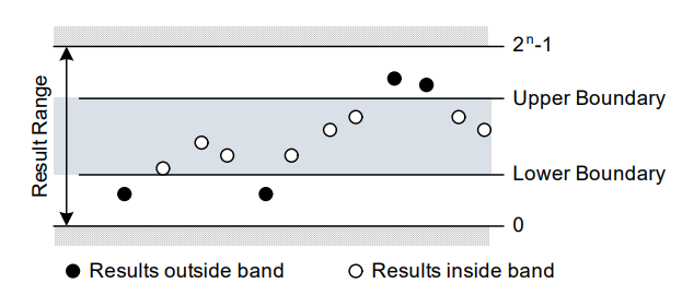
ADC limit detection
In motor control different faults such as over voltage, under voltage, over current, over temperature, etc. can be handled using ADC result monitoring feature with optimum software overhead.
The ADC result monitoring mechanism can automatically compare conversion result to an configured upper and a lower boundary value as shown in the Figure 11 and issue a service requests based on predefined conditions.
Figure 11.
ADC result monitoring through limit checking
Averaging or finite impulse response filters (FIR)
Typically, potentiometer is used for demonstration of motor speed control. Potentiometer sets the analog speed reference set point which is converted by ADC in digital format and process by the MCU. Any noise in the speed reference signal will leads to oscillation in the actual motor speed. Averaging or filter feature of
PSOC™
Control C3 MCU can be used to filter out the unwanted noise from the actual speed set point to avoid the motor speed oscillation. Similarly, these features can be used for temperature sensor and DC bus voltage measurement as well. Noise or fluctuation in these signals can degrade the performance or can result in unstable system behavior.
Averaging can be selected for Group-1, which contains DC bus voltage, temperature sense, and analog speed sense channels. A result is generated and stored every N trigger, as per user configuration.
Ambient temperature measurement
PSOC™
Control C3 MCU has an on-chip temperature sensor that is used to measure the internal die temperature. This on-chip temperature sensor can be used for cost optimized MCU ambient temperature measurement.
The output of the temperature sensor can be routed to SAR ADC through AMUX0 or AMUX1, these correspond to ADC channels 15 and 19, the temperature measurement requires the following ratio:
and can be measured in the following manner:
When either channel 15 or 19 is selected the temperature sensor is biased with a 1 uA current by default, this output corresponds to the measurement
By setting TEMPSENSE_CURRENT_SEL bit to '1' in HPPASS_SAR_CFG_TEMPSENSE_CTRL register, an additional 8 uA flows into the BJT, this corresponds to the measurement
Die temperature can be calculated as given in the following equation:
The constant A, B, C, and D are stored in the registers during factory calibration.
Autonomous controller for motor control
The autonomous controller (AC) provides hardware control without the need for CPU or external intervention.
The AC is a programmable-state machine. Following figure shows the AC simplified block diagram. It consists of a memory-based state transition table, sequencer, and timers.
Figure 12.
Autonomous controller block diagram
Autonomous controller capabilities
The autonomous controller (AC) has the following capabilities:
Enabling and disabling of blocks, providing BLOCK_READY status to the firmware
Ability to be triggered by hardware/firmware and execute programmed actions
Triggering any of the HPPASS internal blocks (SAR groups, CSG slices)
Implementing hardware delays
Taking periodic action (for example, triggering) in a timed loop
Receiving conditions from the HPPASS internal blocks and executing (for example, triggering) on those events
Generating an AC-based interrupt to the CPU
Controlling AROUTE switches (Note: advanced usage only)
Monitoring SAR ADC limit detection condition and taking an action based on the status
AC configuration for 3-shunt FOC
As described in
Figure 6
, 3-shunt FOC algorithm need 6 ADC channels. These 6 channels are divided into two subgroups, Group-0, and Group-1. Group-0 has high-priority and Group-1 has low-priority. In the following state transition table, autonomous controller receive the triggers from timer and trigger ADC conversion for both the group.
STATE:TOP
ACTION=WAIT_FOR   COND=HW_TR0_IN             /* wait for ADC trigger event */

STATE:
SAR_TR=0x01   ACTION= NEXT                   /* Trigger group 0, and jump to next state */

STATE:
ACTION=WAIT_FOR   COND=CNT_DONE   CNT=0x7ff  /* Configure some delay */

STATE:
SAR_TR=0x02   ACTION=NEXT                    /* Trigger Group 1 and jump to next state */

STATE:
ACTION=BRANCH_IF_TRUE   BR_ADDR=TOP   COND=TRUE /* Jump to TOP state */
Note:
The above code fragments are written in an easy-to-read format (versus register writes) in which a state is delimited by the STATE: with optional label, and the code as <FIELD_NAME> = <FIELD_VALUE>, see the
PSOC™
Control C3 MCU architecture reference manual for more details of AC.
Revision history
Document revision | Date | Description of changes |
|---|---|---|
** | 2024-07-04 | Initial release. |
*A | 2024-12-03 | Changed distribution from restricted to public. |