AN239961 Synchronous buck converter with PSOC™ Control C3 MCU
About this document
Scope and purpose
This application note provides information on how a synchronous buck converter can be implemented with PSOC™ Control C3 devices. This document also provides information about power conversion middleware and Power Conversion Configurator (PCC) tool, which is an easy to use software to configure the buck converter. The PSOC™ Control C3M5 Complete System Dual Buck Evaluation Kit along with PCC tool is used as an example to illustrate the implementation of the buck converter in both voltage control mode (VCM) and current control mode (CCM) using PSOC™ Control C3 MCU.
Intended audience
This document is intended for users who are new to PSOC™ Control C3 MCU, PSOC™ Control C3M5 Complete System Dual Buck Evaluation Kit, and PCC tool.
Associated part family
PSOC™ Control C3 devices
Software version
3.3 or above.
Introduction
A buck converter, also referred as "step down converter" is a type of DC-DC converter that generates an output voltage ( ) that is lower than the input voltage ( ). The design of the buck converter is to maintain a stable output voltage regardless of variations in the input voltage or load conditions. Furthermore, buck converters are non-isolating, meaning they share a common ground between the input and output.
Figure 1
shows an asynchronous buck converter circuit diagram.
Figure 1.
Asynchronous buck converter
If better efficiency values are required, replace the rectifying diode (D) by an active switch with a lower voltage drop (resulting in a synchronous buck converter topology). With such a solution, the rectification will be synchronously controlled by a signal that is complementary to the control signal (PWM).
Figure 2
shows the synchronous buck converter circuit diagram.
Figure 2.
Synchronous buck converter
This application note aims to describe the output voltage control of dual buck evaluation kit with voltage control mode (VCM) and peak current control mode (PCCM) in different configurations like single-phase, multi-phase (also known as "interleaved") and multi-instance using PSOC™ Control C3 MCU. It also describes the PCC tool and middleware, developed to generate firmware for different converter topologies with a few mouse clicks. The PSOC™ Control C3 MCU is designed for real-time control application, such as power conversion. Usage of various peripherals which are intended for power conversion application is described in the respective sections of this document.
Key features
The key features of PSOC™ Control C3 MCU, dual buck evaluation kit, PCC tool, and middleware are as follows:
PSOC™ Control C3 MCU:
High performance, low-power, 32-bit single-core Arm® Cortex®-M33 based microcontroller running up to 180 MHz clock frequency. It supports a digital signal processor (DSP), floating point unit (FPU), memory protection unit (MPU), and state-of-the-art security features
High-performance, programmable analog subsystem (HPPASS)
12-bit, 12 Msps SAR ADC block, support 16 analog channels with 16 samplers for synchronous idle sampling
Five analog comparators with <10 ns built-in 10-bit DAC to generate the negative input to the respective comparator
Real-time control peripheral:
Hardware coordinate rotation digital computer (CORDIC) for solving circular (trigonometric), hyperbolic functions, and integrated independent look-up tables to accelerate calculation
Sixteen 16-bit timer, counter, pulse-width modulator (TCPWM)
Four 32-bit TCPWM supporting <80 ps high-resolution pulse width modulation
256 KB read-while-write flash with ECC
64 KB SRAM with ECC support
Communication interface: Six SCB and two CAN FD (one supporting 8 Mbps)
Two DMA controllers with 16 channels each
Supports up to 240 MHz peripheral clock
Up to 50 GPIOs with programmable drive modes, strengths, and slew rates; up to 28 pins support smart I/O programmable logic and up to 18 dedicated analog pins
Dual buck evaluation kit:
Two independent synchronous buck converters that are capable of:
Voltage control mode (VCM) and peak current control mode (PCCM)
Multi-instance/multi-phase (interleaved) synchronous buck converter
Up to four buck channels by connecting a second dual buck evaluation board in a master-slave configuration with a single PSOC™ Control C3M5 Digital Power Control Card
Two onboard variable and transient loads for testing full load and step load responses with the option to connect external electronic loads (e.g., programmable loads) for further advanced testing
Test points for connecting network analyzer for frequency response analysis
Convenient test points for capturing the relevant waveforms (digital and analog) when the buck converter is running
Three LEDs: A POWER LED indicates when the power is supplied, ACT LED or active led indicates when the converter is running, and FAULT LED indicates in case of fault
A general-purpose user button
PCC tool and power conversion middleware:
PCC tool is a graphical user interface (GUI) that combined with the middleware allows to define buck converter operation:
The PCC tool allows to define buck converter parameters, such as input voltage, output voltage, passive components, protection, and control parameters in an easy to use interface
Middleware is the repository of C-level functions used to create the control algorithm that is configured by selection performed in the PCC tool
Support voltage control (VCM) and peak current control mode (PCCM)
Auto-generated control loop and custom (user-defined) control loop modes support
Offers the automatic calculation of regulator coefficients or allows enter coefficient values manually
Generating the frequency response curves for plant, open loop, and compensator according to the converter parameters
For more details on the PSOC™ Control C3 MCU, see the
reference manual
and
datasheet
. For more information on kit and tooling, see the
dual buck evaluation kit
,
PCC tool
, and
middleware
.
Abbreviation and acronyms
The details of abbreviations and acronyms used in the document is given in
Table 1
.
Abbreviation | Description |
|---|---|
ADC | Analog-to-digital converter |
CSG | Comparator and slope generator |
DAC | Digital-to-analog converter |
DSP | Digital signal processor |
FIR | Finite impulse response |
FPU | Floating point unit |
HPPASS | High-performance programmable analog subsystem |
MCU | Microcontroller |
MPU | Memory protection unit |
PCC | Power Conversion Configurator |
PCCM | Peak current control mode |
PWM | Pulse width modulation |
SAR | Successive approximate register |
TCPWM | Timer, counter, and pulse width modulation |
VCM | Voltage control mode |
Buck converter basics
shows a generic block diagram of voltage control mode buck converter. The modulator periodically regulates the duty cycles to maintain the output voltage constant and equal to the reference value. The block diagraswitch-mode power supplym consists of a compensator, the transfer function of which depends on the intended control mode. The compensator's output is then translated into PWM lines by a modulator block and a plant transfer function.
Figure 3.
System control diagram
Compensation:
Action of controlling in the feedback loop a plant quantity, like the output voltage in the buck converter.
Modulation:
Action of translating a numeric field, for example, a duty cycle into a PWM signal.
Voltage control mode vs. peak current control mode
Voltage mode control implies that the output voltage is regulated by direct change in the duty cycle, see
Figure 4
. For detailed information, see the
Voltage control mode buck converter
section.
Figure 4.
Synchronous buck converter with voltage control mode
Peak current mode control implies that the output voltage is regulated by adjusting the peak current flowing through the inductor, PWM is driven by comparison of current in the inductor and an internal generated reference through DAC.
The current mode control features a dual loop circuit: An outer loop to regulate the output voltage and an inner loop to control peak current, see
Figure 5
. For detailed information, see the
Peak current control mode buck converter
section.
Figure 5.
Synchronous buck converter with peak current control mode
compares the advantages and drawbacks of each mode.
Peak current control mode | voltage control mode | |
|---|---|---|
Noise sensitivity For example, voltage and current ripple due to switching | High noise sensitivity | Low noise sensitivity |
Cost | Higher cost | Lower cost |
Resolution | Resolution is limited by the comparator latency and resolution of the internal reference | Resolution is limited by a PWM timer clock |
Easiness of feedback design | Requires slope compensation to reject subharmonic oscillation in case of duty cycle approaches 50% or beyond. | Easy feedback design |
Response to condition changes | Responds immediately to input voltage changes. It cannot handle very wide input voltage variations. | Relatively slow response to input/output condition changes |
Current limiting | Inherent cycle by cycle current limiting | Requires additional current protection (comparator) |
Complexity | More complex | Less complex |
PSOC™ Control C3 MCU
The PSOC™ Control C3 MCU family is designed for real-time control, enhanced sensing, secure, and low-power operation. The MCU includes many peripherals that are especially useful for industrial control, motion control, automation devices, home appliances, switch mode power supply, low-power sensors, etc.
The implementation of a synchronous buck converter solution makes use of the following peripherals of the MCU to achieve optimum performance:
High-performance programmable analog subsystem (HPPASS)
Timer, counter, and pulse width modulation (TCPWM) module
Successive approximate register–analog-to-digital converter (SAR-ADC)
Comparator and slope generator module (CSG)
HPPASS triggers
The following sections provides the detailed description of the peripheral information for the synchronous buck converter solution.
TCPWM generation
The timer, counter, and PWM (TCPWM) block is a multipurpose timer unit for signal monitoring/conditioning and pulse width modulation (PWM) signal generation. It is designed with repetitive structures with multiple timers that have the same base functionality. The internal modularity of the TCPWM translates into software easy to use system for fast code development and portability between applications. TCPWM block consist of three groups (Group 2-0): Group-0 has four 32-bits counters, Group-1 has eight 16-bit counters along with Motion interface (MOTIF) block, and Group-2 has eight 16-bit counters.
TCPWM key features:
Three counter group:
Group 1 and Group 2 support up to 8 counters. Group 0 supports up to 4 counters
Each counter can run in one of the four function modes:
Timer-counter with compare
Timer-counter with capture
Pulse-width modulation
PWM with dead-time
Each group works in left align, right align, center align, asymmetric, asymmetric CC0 and CC1, and center asymmetric CC0 and CC1 modes
A configurable motion interface module can operate in four different modes: quadrature decoder, Hall sensor, stand-alone multi-channel mode, and quadrature mode with stand-alone multi-channel
Supports high-resolution PWM (HRPWM) generation feature in 32-bit TCPWM counters
16- or 32-bit counter, 2 compare/capture (CC0/CC1), and period registers
Up, down, and up/down counting modes
Rising edge, falling edge, combined rising/falling edge detection, or pass-through on all hardware input signals to derive counter events
The start, reload, stop, capture0, and capture1 events can be generated by software
Two output trigger signals for each counter to indicate underflow, overflow, CC0_match, CC1_match. CC0_CC1_match, LINE_OUT, and TC events
Both the period and compare registers have shadow registers
Two PWM complementary output lines for each counter. Dead-time insertion could be 8 bits or 16 bits and independent for two PWM outputs per design configuration
Kill functionality with multiple features to adjust the PWM generation according to the different use cases
HRPWM generation
The HRPWM enhancement allows higher resolution control for power conversion applications. The high resolution PWM generator is an essential module for cutting edge/optimized switch-mode power supply applications development.
The high-resolution generation is only applicable to Group 0 32-bit counters
Supports buffer registers for period, duty cycle, and dead-time for shadow update purpose
Supports <80 ps high-resolution PWM
The HRPWM generation feature is supported in PWM and PWM_DT mode only
To control the high-resolution extension, adjust the lowest six bits of the relevant TCPWM registers
Supports the following PWM outputs: Right align, left align, center align, asymmetric with CC0, asymmetric with CC0 and CC1, and center align asymmetric with CC0 and CC1 for HRPWM features
HPPASS - SAR ADC
The high-performance programmable analog subsystem (HPPASS) can sense voltage and convert it into a digital value, post process the ADC, and therefore, makes first-level decisions as close to the signal source as possible. It can store the processed decision/data and autonomously stream the data to the CPU. It can also operate autonomously (independent of the CPU) with the help of an autonomous controller.
The PSOC™ Control C3 MCU HPPASS has the following features:
A 12-bit SAR ADC
Comparator and slope generators (CSG)
Digital-to-analog converter (DAC)
Autonomous controller (AC)
Input triggers, output level triggers, output pulse triggers
The functionalities of SAR ADC that are useful for digital power control includes:
When converting a single channel, the maximum speed of the ADC is 12 Msps
16 samplers, including 12x direct connections, and 4x muxed connections, which can produce simultaneous sampling of external analog signals
21 channels: 16 external analog inputs, two channels multiplexed with GPIOs, and three channels assigned to internal signals
Up to eight conversion sequence. Every sequence can be triggered by firmware, TCPWM, GPIO, SMARTIO, or autonomous controller
Multiple interrupt generation options from – scan group done, FIR done, and FIFO level, FIFO overflow/underflow, limit detection, result overflow
A 32-entry FIFO that can be subdivided into 1, 2, or 4 FIFOs
HPPASS CSG
With five high-speed comparators and a slope generator (CSG), it is possible to address several power conversion topologies with reduced software interaction. The main features of a comparator and DAC are as follows:
Each CSG slice consists of a 10-bit, 30 Msps DAC, and a 10 ns latency comparator
Each comparator positive input can select one of the two analog inputs and the negative input can select the DAC output or one of the two analog inputs
Multiple interrupt generations from - comparator output, DAC hardware started, DAC slope done, DAC buffer empty
DAC supports multiple modes:
Direct write mode
Buffered mode
Hysteretic mode
Slope generation mode
LUT waveform generation mode
Comparator post processing includes:
Configurable comparator output polarity
Blanking the comparator output
Deglitching the comparator output
Generate a configurable comparator interrupt or AC trigger
Ability to select the comparator output or inverted comparator as an update trigger
HPPASS triggers
Eight input triggers, which can configure to a firmware-level trigger, a firmware pulse trigger, hardware trigger A (multiplexer trigger), or hardware trigger B (one-to-one trigger)
Eight output level triggers, each of which can select a CSG comparator output and a SAR ADC limit detection output
Eight output pulse triggers, each of which can select one pulse trigger from ADC group done, FIR done, and AC trigger
For a detailed description of all the peripherals of the MCU, see the
reference manual
.
PSOC™ Control C3M5 Complete System Dual Buck Evaluation Kit
PSOC™ Control C3M5 Complete System Dual Buck Evaluation Kit demonstrates the wide capabilities of the PSOC™ Control MCUs.
The kit comprises of:
Dual buck evaluation board
PSOC™ Control C3M5 Digital Power Control Card
USB Type-A to Type-C cable
24 V DC power adapter
24-pin daisy chain ribbon cable
Quick start guide
Voltage control mode (VCM) and peak current control mode (PCCM) with slope compensation are supported in multiple configurations, such as single-phase, multi-instance, and multi-phase, allowing you to test MCU features in multiple scenarios.
For more details on the implementation of the digital buck converter in voltage mode and peak current mode control, see the
Voltage control mode buck converter
and
Peak current control mode buck converter
sections respectively. The software project are developed using the
ModusToolbox™
platform.
Specifications
The dual buck evaluation board is targeted for low voltage applications.
Table 3
shows the specifications. See the
user guide
for the schematic diagram of the buck converter stage. By default, the target output voltage and current for both buck circuits is 5 V and 1.2 A maximum IOUT in variable load mode, and 5 V and 2 A maximum IOUT in transient load mode. Nevertheless, as a buck converter, any voltages close to VIN is theoretically possible depending on the driving of the MOSFETs duty cycle.
The inductor value ensures continuous conduction mode (CCM) of the buck converter as far as the 2-pin headers J6 for BUCK1 (24 Ω) and J9 for BUCK2 (24 Ω) are short. In other words, DCM operation occurs only when headers J6 for BUCK1 or J9 for BUCK2 are open, assuming a 400 kHz switching frequency.
Specification | Name | Values |
|---|---|---|
Input voltage | VIN | 24 V DC |
Output voltage | BUCK1_VOUT BUCK2_VOUT | 5 V DC 5 V DC |
Maximum output current | BUCK1_IOUT_max BUCK2_IOUT_max | 1.2 A in variable load and 2 A in transient load 1.2 A in variable load and 2 A in transient load |
Multiphase mode (Short header J14) | VOUT IOUT | 5 V DC 2.4 A in variable load and 4 A in transient load |
The dual buck evaluation board is designed to be operated with an input voltage up to 45 volts. However, the power adapter included in the kit provide 24 volts only.
Specification | Name | Value |
|---|---|---|
Main inductor | BUCK1 L2 BUCK2 L2 | 47 uH 47 uH |
Output capacitor | BUCK1 C15 | | C16 | | C19 BUCK2 C31 | | C32 | | C33 | 47 uF| |47 uF| |22 uF = 116 uF 47 uF| |47 uF| |22 uF = 116 uF |
Gate driver high and low side | BUCK1 U2 BUCK2 U3 | 2EDL8023GXUMA1 |
MOSFETs | BUCK1 Q1, Q2 BUCK2 Q3, Q4 | IPD122N10N3GATMA1 |
Specification | Header | Name | Value |
|---|---|---|---|
Set SW4 to variable load position | Header J5 SHORT and header J6 SHORT | BUCK1_IOUT varies from | 0.2 A to 1 A |
Set SW4 to transient load position | Header J5 SHORT and header J6 SHORT | BUCK1_IOUT toggle between | 0.2 A to 1.8 A |
Set SW5 to variable load position | Header J8 SHORT and header J9 SHORT | BUCK2_IOUT varies from | 0.2 A to 1 A |
Set SW5 to transient load position | Header J8 SHORT and header J9 SHORT | BUCK2_IOUT toggle between | 0.2 A to 1.8 A |
For more information related to switches and jumpers position on board, are shown in
Figure 7
.
System block diagram
This section provides a brief description of the complete system block diagram of the PSOC™ Control C3M5 Dual Buck Evaluation Kit (KIT_PSC3M5_DP1). see
Figure 6
.
Figure 6.
PSOC™ Control C3M5 Complete System Dual Buck Evaluation Kit system overview
KIT_PSC3_DB1 Dual Buck Evaluation Board
Features of the KIT_PSC3_DB1 Dual Buck Evaluation Board (see
Figure 7
) includes:
Two independent synchronous buck converters
Provision for multiple topologies, such as single-phase, multi-instance, and multi-phase
Onboard transient and variable load circuits – one for each buck circuit
Variable load can go from 0.2 A to 1 A
Transient load can switch between 0.2 A to 1.8 A
Option to connect to four buck channels by connecting a second dual buck evaluation board in a master-slave configuration with a single PSOC™ Control C3M5 Digital Power Control Card
Master slave connectors for controlling a second dual buck evaluation board with a single PSOC™ Control C3M5 Digital Power Control Card
Figure 7.
KIT_PSC3_DB1 Dual Buck Evaluation Board
PSOC™ Control C3M5 Digital Power Control Card
Features of the PSOC™ Control C3M5 Digital Power Control Card (KIT_PSC3M5_CC1, see
Figure 8
) includes:
PSOC™ Control C3M5 (Arm® Cortex®-M33 based) MCU PSC3M5FDS2AFQ1, 180 MHz, up to 256 KB flash/64 KB SRAM, E-LQFP-80
Connection to dual buck evaluation board (applicable to other boards) via card edge header
Onboard J-Link debugger and UART virtual COM port with Micro-USB connector
Test points for debugging purpose
Figure 8.
PSOC™ Control C3M5 Digital Power Control Card
Software ecosystem
Infineon provides the
ModusToolbox™
software for firmware/application development based on PSOC™ Control C3 MCUs. ModusToolbox™ software is a modern, extensible development ecosystem supporting a wide range of Infineon microcontroller devices, including PSOC™ Arm® Cortex® MCUs, TRAVEO™ T2G Arm® Cortex® MCU, XMC™ Industrial MCUs, AIROC™ Wi-Fi devices, AIROC™ Bluetooth® devices, and USB-C Power Delivery MCUs. This software includes configuration tools, low-level drivers, middleware libraries, and other packages that enable you to create MCU and wireless applications. All tools run on Windows, macOS, and Linux. ModusToolbox™ includes an Eclipse IDE, which provides an integrated flow with all the ModusToolbox™ tools. Other IDEs such as Visual Studio Code, IAR Embedded Workbench, and Arm® MDK (μVision) are also supported.
ModusToolbox™ software supports stand-alone device and middleware configurators. Use the configurators to set the configuration of different blocks in the device and generate code that can be used in firmware development.
Libraries and enablement software are available on the
GitHub
site.
ModusToolbox™ can be interfaced through the command line. See the "ModusToolbox™ build system" section in the
ModusToolbox™ tools package user guide
for detailed documentation.
Installing the ModusToolbox tools package
Configurators
ModusToolbox™ software provides graphical applications called "configurators" that make it easier to configure a hardware block. For example, instead of having to search through all the documentation to configure a Serial Communication Block (SCB) as a UART with a desired configuration, open the appropriate configurator and set the baud rate, parity, and stop bits. After saving the hardware configuration, the tool generates the "C" code to initialize the hardware with the desired configuration.
There are two types of configurators: BSP configurators that configure items that are specific to the MCU hardware and library configurators that configure options for middleware libraries.
Configurators are independent of each other, but they can be used together to provide flexible configuration options. They can be used as stand-alone, in conjunction with other tools, or within a complete IDE. Configurators are used for:
Setting options and generating code to configure drivers
Setting up connections such as pins and clocks for a peripheral
Setting options and generating code to configure middleware
A few configurators available for PSOC™ Control C3 MCU are:
Device Configurator
: Set up the system (platform) functions, pins, and the peripherals (e.g., HPPASS, LPCOM, PWM, SCB)
Power Conversion Configurator
: Configures the power stage converter and generates the required code. Install ModusToolbox™ Industrial MCU pack from
Infineon Developer Center
to use the Power Conversion Configurator (PCC) tool
Smart I/O Configurator
: Configure smart I/O pins
Each of the above configurators creates their own files (e.g.,
design.modus
for Device Configurator). The configurator files (
design.modus
) are usually provided with the BSP. When an application is created based on a BSP, the files are copied into the application. You can also create custom device configurator files for an application and override the ones provided by the BSP.
ModusToolbox help
The ModusToolbox™ ecosystem provides documentation and training. Launch the Eclipse IDE for ModusToolbox™ software and navigate to the following Help menu items:
Choose Help >
ModusToolbox™ General Documentation:
ModusToolbox™ Documentation Index:
Provides brief descriptions and links to various types of documentation included as part of the ModusToolbox™ software
ModusToolbox™ Installation Guide:
Provides instructions for installing the ModusToolbox™ software
ModusToolbox™ User Guide:
This guide primarily covers the ModusToolbox™ aspects of building, programming, and debugging applications. Additionally, covers various aspects of the tools installed along with the IDE
ModusToolbox™ Training Material:
Links to the training material are available at https://github.com/infineon/training-modustoolbox
Release Notes:
Describes the features and known limitations for the ModusToolbox™ software provided as part of the ModusToolbox™ tools package included with the installer
For documentation on Eclipse IDE for ModusToolbox™, choose
.
User Guide:
Provides descriptions about creating applications as well as building, programming, and debugging them using the Eclipse IDE
Eclipse IDE Survival Guide:
This is a link to a forum with answers for questions about how to get common tasks done
Power Conversion Configurator (PCC) tool
Install the Power Conversion Configurator (PCC) tool from the
ModusToolbox™ Industrial MCU Pack
. For more details of the tool, see the Power Conversion Configurator
user guide
.
The PCC tool is used along with the ModusToolbox™ software intended to generate data structures to configure middleware for provided power-supply design inputs. Its purpose is to offer a framework for estimating and showcasing the expected performance characteristics of a converter.
The tool provides the capabilities to initially configure a switched-mode step-down DC-to-DC converter with the buck topology. Various parameters such as input voltage, output voltage, passive components, protection, and control parameters are easily configured with an easy to use interface. Subsequently, the configurator generates a basic schematic diagram, a Bode plot for user reference, and calculates the controller coefficient values to facilitate the execution of a control loop in the firmware implementation.
The generated firmware will appear in the
cycfg_pwrconv.h
and
cycfg_pwrconv.c
files. The generated files are in the
Generated Source
folder next to the
.modus
file, which contains the user configuration.
Middleware
The Power Conversion Middleware (mtb-pwrconv) consists of the device-agnostic top-level API source code, the power conversion library source code, and the solution personality. Middleware provides integration with the Power Conversion Configurator tool, integration with the Device Configuration tool, generates the power conversion regulator configuration code, and the device-specific hardware configuration code.
The middleware can be added to the project with the help of the library manager. Information regarding how to use a library manager is given in the
ModusToolbox™ Library Manager user guide
.
Voltage control mode buck converter
The voltage control mode in a buck converter is a control strategy used to regulate the output voltage of the converter. The steady state function of a buck converter voltage control is based on . In this mode, the converter operates by adjusting the duty cycle (D) of the power switch to maintain a constant output voltage, despite changes in the input voltage or load current.
The buck converter has a feedback loop that continuously monitors the output voltage and compares it to a reference voltage. If the output voltage deviates from the reference voltage, the controller adjusts the duty cycle of the power switch to increase or decrease the energy transferred to the output. This, in turn, adjusts the output voltage to bring it back to the desired level.
Figure 9
shows the block diagram of buck converter - single-phase in voltage control mode.
The start of the conversion is triggered when the terminal count in the TCPWM slice occurs. Once the conversion result is available, an interrupt service request (ISR) is activated, and the voltage control function is executed in software (H(z)-3P3Z). This function updates the TCPWM slice compare register. A safe update with no glitches on the PWM output is possible due to the shadow transfer update that happens at the terminal count event.
Figure 9.
VCM buck converter - single-phase topology
Timing scheme:
The SAR ADC will start sampling at the terminal count event of the PWM signal and the CPU will execute the control algorithm in ISR triggered by ADC group conversion done event. In voltage control mode, the sensing of inductor current is not required. The waveform of the inductor current is shown in
Figure 10
.
Figure 10.
Voltage control mode with PSOC™ Control MCU - generic timing diagram
Compensator design (3P3Z)
The aim of the compensator in the system is to regulate the output voltage irrespective of the presence of noise, disturbances, and modeling errors. A type-3 (3 poles, 3 zeros) filter is one of the most suitable feedback controllers for voltage-controlled buck converters. Place the poles and zeros of the compensation networks according to the analysis of the control-to-output transfer function, see
Figure 11
for reference.
Type 3 filters have 3 poles and 2 zeros implementing the following transfer function in a continuous time domain (H(s)):
To allow the MCU using the compensator transfer function, a discrete time transformation is needed following the bilinear approach:
Having:
Which, in a linear difference equation:
Where x[n] = reference - feedback
Figure 11.
Designing a type 3 compensator
Voltage control mode implementation
Two boards PSOC™ control C3M5 Power Control Card and dual buck evaluation board are used for the implementation of voltage control mode. The voltage control loop is implemented for single-phase by a classic 3 poles, 3 zeros filter using floating-point values. The filter coefficients are provided and have been selected to have the following controller characteristics:
Switching frequency = 300 kHz
Crossover frequency = 7 kHz
Phase margin = 50 degrees
PWM master clock = 240 MHz*64 (6-bits for HRPWM)
PWM resolution = <80 ps
ADC resolution =12-bits
SAR-ADC group conversion is continuously triggered by the terminal count of TCPWM (set to period value, although you can configure it accordingly).
Once the output voltage has being measured by the SAR-ADC, a group done interrupt is generated. Inside the ISR, the 3 poles, 3 zeros controller are applied and the value for the duty cycle is updated.
Control specification
The Power Conversion Configurator tool allows you to easily specify the different characteristics of a power system to define the related compensator coefficient and theoretical frequency response.
Configure the following parameters using the PCC tool:
The control mode
Coefficient for controller
Switching frequency
Phase margin and crossover frequency
Buck converter parameters - L, C, Vout, Vin, Iout
Blanking time for PWM
Protection parameters and limits
Ramp up time
Pre/post processing function for the system, etc.
For detailed information, see
PCC tool
and
middleware
documents.
Design at peripheral level
Figure 12.
VCM - peripheral interconnectivity for single phase buck converter
shows the peripheral internal-connection diagram for a single phase buck converter in voltage control mode. By using the same concept and other set of peripherals (shown in
Table 8
and
Table 9
), interleaved or multi-instance for 'n' number of buck converters in voltage control mode can also be implemented using a few mouse clicks with the help of PCC tool, Device Configurator, and middleware.
Solutions configuration
The Device Configurator has a tab called "Solutions". The buck converter instances can be added with the help of the '+' symbol and removed by deselecting the check box.
Figure 13
shows the solution tab configuration. The same configuration can be used to configure buck converter with voltage control mode in single-phase topology.
Note:
To make the
Solutions
tab visible, add the power conversion middleware (
mtb-pwrconv
) from Library Manager.
Figure 13.
Solutions tab configuration
A. Solutions:
This tab is used to configure the buck converter instance.
B. Buck converter:
This section shows the active buck converter instance and its configuration PWM, ADC, etc.
C. External Tools:
Button to Launch Power Conversion Configurator tool.
D. Modulator:
It represents the control mode and number of the phases of the active buck converter instance.
E. PWM:
It represents the configuration related to PWM clock, dead-time, switching frequency, passive level output, and option to invert the (high-side/low-side) PWM outputs.
F. Phase 0:
PWM pin and group configuration section to configure the PWM group, counter, and pin numbers.
G. ADC:
ADC channel configuration section to configure the ADC pins.
H. Controller:
This section provides the name of the pre/post processing functions and header files.
I.
Internal Routing:
This section represents the automatically configured output and input triggers according to the above configurations.
Power Conversion Configurator
PCC tools configurations are explained in the following section and comes under the tool bar view. The same configuration can be used to configure buck converter with voltage control mode in single-phase topology.
Converter configuration
shows the converter tab and information of various features are as follows:
Figure 14.
VCM - Converter tab configuration
A. Control mode:
It represents the control mode of the active instance of the buck converter.
B. Buck converter configuration:
Selection of the passive elements values, the target output current, the input, and output voltage.
C. Modulator block:
Press this block to open the modulator tab.
D. Control loop block:
Press this block to open the controller tab.
E. ADC block:
Press this block to jump to the ADC tab.
F. Control parameters:
It configures the number of phases, switching frequency, time delay of buck converter. It also helps to configure the crossover frequency and phase margin.
G. Compensation settings:
It represents the automatically generated poles and zeros of the compensator based on converter configuration. It also provides the options to overwrite the automatic generation by selecting the
Manual
approach and define the poles and zeros manually.
Modulator configuration
shows the modulator tab and information of various features are as follows:
Figure 15.
VCM - Modulator tab configuration
A. PWM instance:
It represents the PWM instance information, such as group, counter number, and pins.
B. Additional PWM configuration:
It configures the dead-time in (ns) between the complementary PWM signals. It also configures the minimum and maximum duty of the PWM signals.
C. Waveforms:
This window gives a pictorial representation of the PWM signals and current waveforms according to configurations.
ADC configuration
shows the ADC tab and information of various features are as follows:
Figure 16.
VCM - ADC tab configuration
A. ⨁ ⊖:
Options to add and remove the ADC channel. To change the channel, it can be done in the
Solutions
tab's ADC section (G), see
Figure 13
.
B. Trigger source:
It configures the conversion trigger source to ADC channel. There are two options, control loop or scheduler.
C. Channel:
It configures the name of the ADC channel.
D. Units:
The units of the measurement of the respective signals. It gives options, such as Volts (V), Amperes (A), and degrees(º).
E. External gain:
It define the attenuation factor to translate the actual quantity in to the equivalent input voltage to the analog pin of the microcontroller.
F. Pin:
It represents the ADC pins, which is configured to measure the respective signals.
G. Protection:
It configures the protection like under and over limits of signals.
Controller configuration
shows the controller tab and information of various features are as follows:
Figure 17.
VCM - Controller tab configuration
A. Controller:
It represents the compensator coefficient generated by the tool according to the configuration. You can copy the coefficient if required.
B. Ramp settings:
It configures the duration and slope of the soft starting period.
C. Pre-processing:
To enable/disable and give the name to the pre-processing user-defined function.
D. Infineon Control Loop:
To enable/disable the Infineon control loop algorithm.
E. Post-process callback:
To enable/disable and give name to the post-processing user-defined functions.
F. Custom Control Loop:
To enable/disable the custom user-defined control loop.
Bode plots
The Bode plots are shown in the separate view. To open the Bode plot, click the view tab, and then Bode plot to analyze the frequency response.
Figure 18
shows the Bode plot and information of various features are as follows:
Figure 18.
VCM - Bode plot
A. Bode plot options:
To hide the legend, zoom in, zoom out, and reset zoom in the Bode plots.
B. Gain plot:
Gain Plot of the system according to the configurations.
C. Phase plot:
Phase plot of the system according to the configurations.
D. Options:
To enable/disable the plant, compensator, and open loop plots.
3P3Z filter implementation
The voltage control loop is implemented by a classic 3 poles 3 zeros filter using floating point values.
Code Listing 1
shows the generated compensator code.
Code Listing 1
__STATIC_FORCEINLINE cy_rslt_t mtb_pwrconv_3p3z_float_process(mtb_stc_pwrconv_reg_3p3z_float_ctx_t * ctx,
                                                      int32_t input, uint32_t * output)
{
float32_t a; /* Accumulator */

/* Filter calculations */
a  = ctx->cfg.b[3] * ctx->dat.i[2]; ctx->dat.i[2] = ctx->dat.i[1];
a += ctx->cfg.b[2] * ctx->dat.i[1]; ctx->dat.i[1] = ctx->dat.i[0];
a += ctx->cfg.b[1] * ctx->dat.i[0]; ctx->dat.i[0] = (float32_t)input;
a += ctx->cfg.b[0] * ctx->dat.i[0];
a += ctx->cfg.a[3] * ctx->dat.o[2]; ctx->dat.o[2] = ctx->dat.o[1];
a += ctx->cfg.a[2] * ctx->dat.o[1]; ctx->dat.o[1] = ctx->dat.o[0];
a += ctx->cfg.a[1] * ctx->dat.o[0];

/* Anti-windup limitations */
a = (a < ctx->cfg.max) ? a : ctx->cfg.max;
a = (a > ctx->cfg.min) ? a : ctx->cfg.min;

ctx->dat.o[0] = a;
*output = (uint32_t)a;

return MTB_PWRCONV_RSLT_SUCCESS; /* For future capability */
}
Interrupt service routine implementation
The
BUCK1_ctrloop_isr ()
routine is used to apply the filter to the ADC measured value and update the TCPWM compare values.
The ADC data will be read inside the ISR and the 3P3Z filter inline function will be called. The filter function produces a 32-bit value to write into the PWM compare register. In the 32-bit value, the upper 26 bits (b31 to b6) are low-resolution data for the HRPWM compare register and the lower 6 bits are the high-resolution data.
Code Listing 2
void BUCK1_ctrloop_isr(void)
{
HPPASS_SAR_RESULT_INTR(HPPASS) = CY_HPPASS_INTR_SAR_RESULT_GROUP_0;
(void) BUCK1_get_error(*CY_HPPASS_SAR_CHAN_RSLT_PTR(0));
buck1_pre_process_callback(); /* Pre-processing callback */
(void) mtb_pwrconv_3p3z_float_process(&BUCK1_regCtx, (int32_t)BUCK1_ctx.err, &BUCK1_ctx.mod);
TCPWM_GRP_CNT_CC0_BUFF(TCPWM0, TCPWM_GRP_CNT_GET_GRP(0U), 0U) = BUCK1_ctx.mod;
}
Execution time of the interrupt service routine and
filter:
shows the experimental results for the execution time of control loop and 3P3Z filter:
Compiler:
ARM_GCC
Optimization:
-Og
Functions | Timings |
|---|---|
BUCK1_CtrLoop_Isr () | 250 CPU cycles (1.4 ) |
3P3Z filter function | 78 CPU cycles (0.434 ) |
Resource allocation - single-phase
The PSOC™ Control C3 MCU peripheral allocated for a typical single-phase voltage control mode solution are captured in
Table 7
.
Peripheral | Usage | Resource allocation |
|---|---|---|
TCPWM | PWM_BUCK_1: HRPWM generation for Buck 1, 32-bit resolution | TCPWM-G0-C0 |
SOFT_START_COUNTER: Used for soft starting purpose, 16-bit resolution | TCPWM-G2-C0 | |
SAR ADC | BUCK1_VOUT: Buck 1 output voltage | AN_A0 |
BUCK1_IOUT: Buck 1 inductor current (optional) | AN_A6 | |
VIN: Input voltage (optional) | AN_A7 | |
BUCK1_TEMP: Buck 1 temperature (optional) | AN_B5 | |
Group 0: Buck 1 | – | |
Interrupt controller (NVIC) | : Group 0 conversion done interrupt | – |
: Timer under flow interrupt for ramp up | – |
Multi-instance implementation
The multi-instance buck converter configuration is also called "single input multiple output configuration". The primary goal of this configuration is to produce multiple, non-isolated, regulated output voltages from a single DC input voltage. This configuration helps in reducing the number of components and overall system complexity while maintaining high efficiency. Each stage operates independently to regulate its specific output voltage.
In this implementation, a single input and two outputs are configured to give a 5 volt output voltage. The converters are working in 180° out of phase.
Figure 19
shows the block diagram of buck converter - multi-instance in voltage control mode.
Figure 19.
VCM buck converter - multi-instance topology
Resource allocation - multi-instance
The PSOC™ Control C3 MCU peripheral allocated for a typical multi-instance voltage control mode solution are captured in
Table 8
.
Peripheral | usage | Resource allocation |
|---|---|---|
TCPWM | PWM_BUCK_1: HRPWM generation for buck 1, 32-bit resolution | TCPWM-G0-C0 |
PWM_BUCK_2: HRPWM generation for buck 2, 32-bit resolution | TCPWM-G0-C1 | |
SOFT_START_COUNTER: Used for soft starting purpose, 16-bit resolution | TCPWM-G2-C0 | |
SAR-ADC | BUCK1_VOUT: Buck 1 output voltage | AN_A0 |
BUCK2_VOUT: Buck 2 output voltage | AN_A5 | |
BUCK1_IOUT: Buck 1 inductor current (optional) | AN_A6 | |
VIN: Input voltage (optional) | AN_A7 | |
BUCK2_IOUT: Buck 2 inductor current (optional) | AN_B4 | |
BUCK1_TEMP: Buck 1 temperature (optional) | AN_B5 | |
BUCK2_TEMP: Buck 2 temperature (optional) | P8.0 | |
Group 0: Buck 1 | – | |
Group 1: Buck 2 | – | |
Interrupt controller (NVIC) | : Group 0 conversion done interrupt | – |
: Group 1 conversion done interrupt | – | |
: Timer under flow interrupt for ramp up. | – |
Multi-phase implementation
The multi-phase buck converter configuration is also called "interleaved buck converter". The primary goal of this configuration is to reduce the size of the filter components. Additionally, it increases the output power of the converter by doubling the current while maintaining the same output voltage. This is equivalent to a parallel combination of two sets of switches, diodes, inductors, and capacitors connected to a common load bank. This configuration helps in reducing the ripple current in the input and out, making it easier to design the input and output filters.
In this example, interleaving is achieved with two buck converters to give a 5 volt output voltage. The converters are working in 180° out of phase, producing inductor currents that are also 180° out of phase (for two-phase).
Figure 20
shows the block diagram of buck converter - multi-phase in voltage control mode.
Figure 20.
VCM buck converter - multi-phase topology
Resource allocation - multi-phase
The PSOC™ control C3 MCU peripheral allocated for a typical multi-phase (two phase) voltage control mode solution are captured in
Table 9
.
Peripheral | usage | Resource allocation |
|---|---|---|
TCPWM | PWM_BUCK_1: HRPWM generation for buck 1, 32-bit resolution | TCPWM-G0-C0 |
PWM_BUCK_2: HRPWM generation for buck 2, 32-bit resolution | TCPWM-G0-C1 | |
SOFT_START_COUNTER: Used for soft starting purpose, 16-bit resolution | TCPWM-G2-C0 | |
SAR-ADC | BUCK1_VOUT: Buck 1 output voltage | AN_A0 |
BUCK1_IOUT: Buck 1 inductor current (optional) | AN_A6 | |
VIN: Input voltage (optional) | AN_A7 | |
BUCK2_IOUT: Buck 2 inductor current (optional) | AN_B4 | |
BUCK1_TEMP: Buck 1 temperature (optional) | AN_B5 | |
Group 0: buck 1 | – | |
Interrupt controller (NVIC) | : Group 0 conversion done interrupt | – |
: Timer under flow interrupt for ramp up. | – |
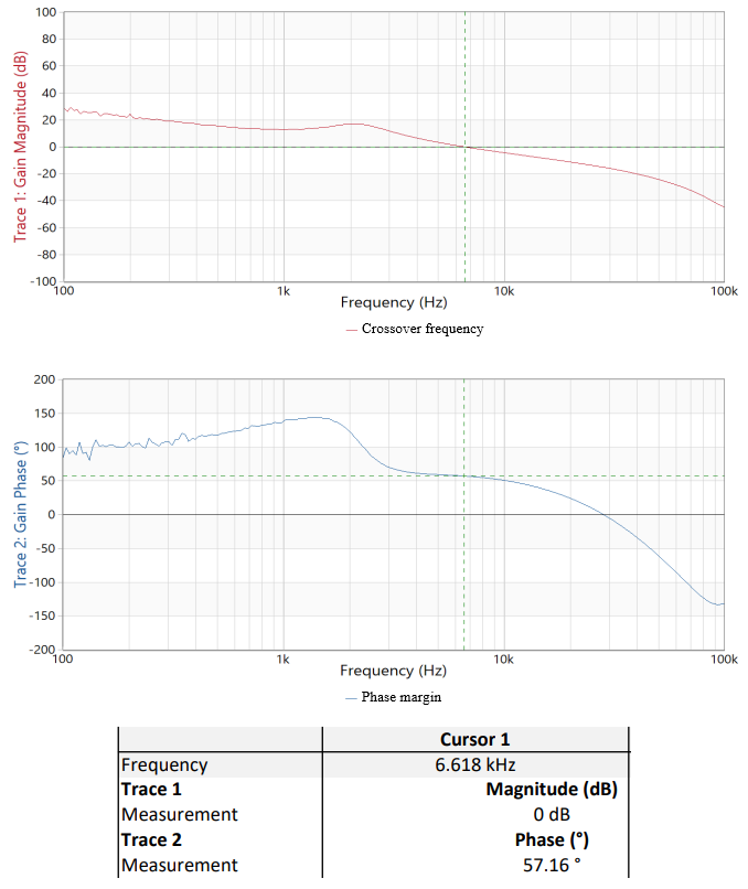
Bode plot and transient response
The Bode plot and waveforms of one phase in voltage control mode is shown in
Figure 21
and
Waveforms
. Stability of the buck voltage mode control is checked using an OMICRON Bode 100 device. The measured phase margin is about 57.16 degrees, and the crossover frequency is 6.618 kHz.
For the setup of the Bode 100 network analyzer, see the
OMICRON Bode 100 kit guide
and the
PSOC™ Control C3M5 Complete System Dual Buck Evaluation Kit user guide
.
Frequency analysis
Figure 21.
VCM Bode plot
Waveforms
Figure 22.
Voltage control mode - variable load
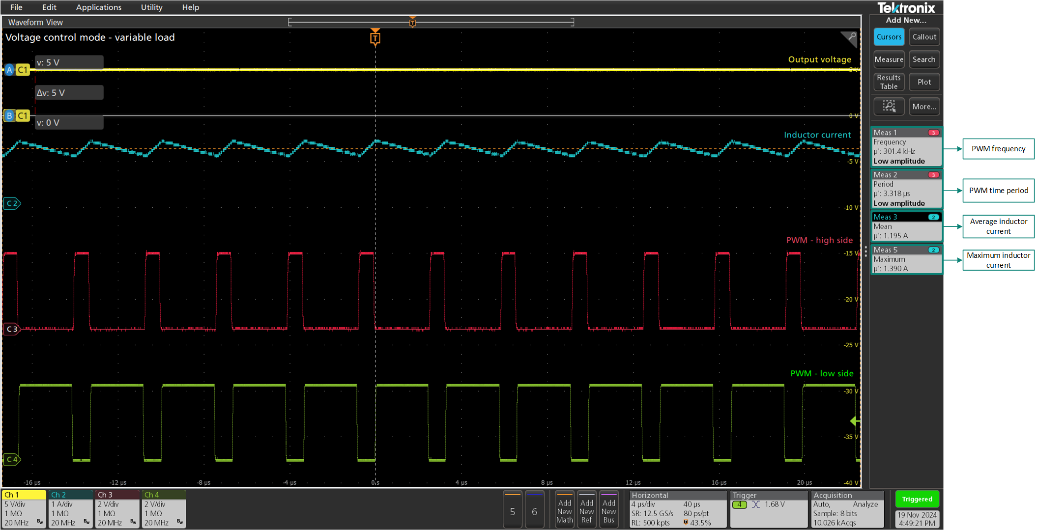
The reference output voltage is 5 volts.
Figure 22
shows the output voltage waveform in maximum load condition. The output voltage is steady at 5 V with the PWM frequency of 300 kHz. The average inductor current is 1.195 A but the maximum inductor current is 1.39 A.
Figure 23.
Voltage control mode - transient load - overshoot
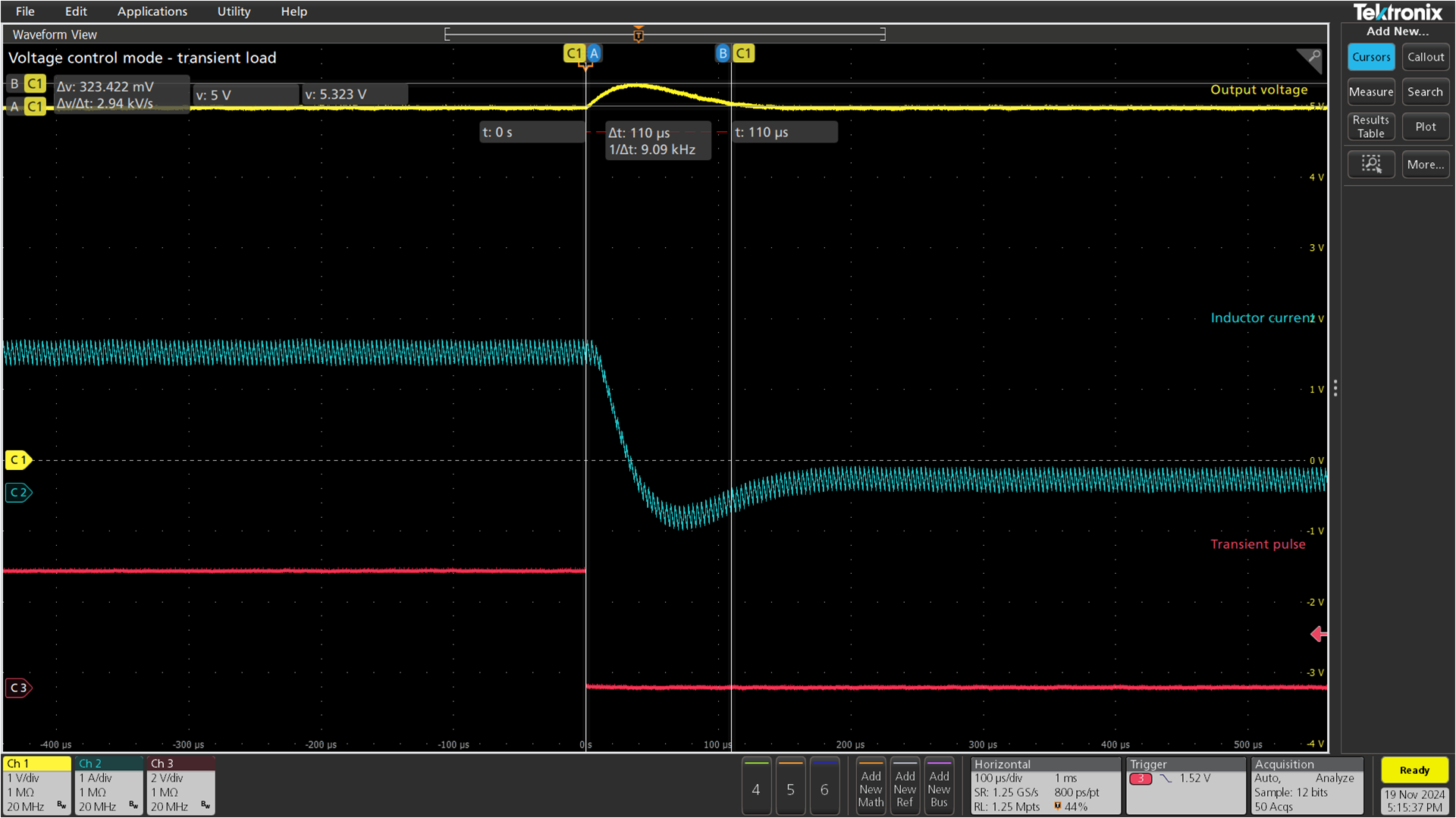
The output voltage waveform at a transient load condition (overshoot) is shown in the Figure 23. Due to the sudden change in load, the overshoot in voltage is 323.422 mV and settling time is 110 μs.
Figure 24.
Voltage control mode - transient load - undershoot
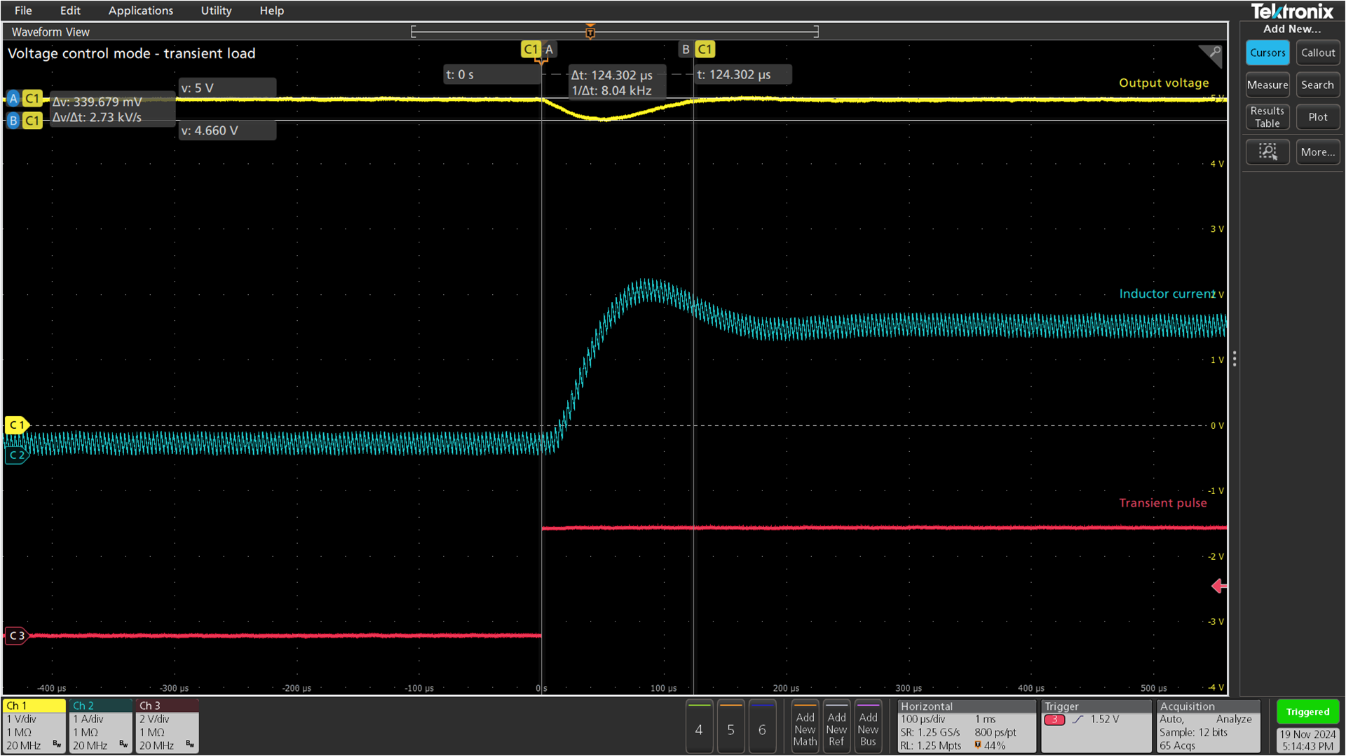
The output voltage waveform at a transient load condition is shown in the Figure 24. Due to the sudden change in load, the overshoot in voltage is 339.679 mV and settling time is 124.302 μs.
Peak current control mode buck converter
During peak current control, the output voltage is maintained by two essential loops:
A digital voltage control loop executed at a defined control frequency which updates the peak current reference
An analog current control loop based on DAC and comparator is provided in the analog peripheral of the PSOC™ Control C3 device
The peak current control mode works by continuously monitoring the high-side switch current through the use of a current transformer (CT). The microcontroller compares the high-side switch current to a predetermined peak current limit. When the high side switch current reaches this limit, the controller turns off the switch, disconnecting the input voltage from the inductor. The switch remains off until the start of the next cycle. At this point, the controller turns the switch back on, reconnecting the input voltage to the inductor, and the cycle repeats. This process is known as a switching cycle and it is repeated continuously to regulate the output voltage.
Figure 25
shows the block diagram of buck converter - single phase in peak current control mode.
The peak current control mode has advantages, including fast transient response, good stability, and overcurrent protection. The peak current control mode stability can be affected by sub-harmonic oscillation if slope compensation is not used. Slope compensation adds an extra complexity that can be solved using the HPPASS-CSG block of PSOC™ Control C3 MCU.
Note:
During the "on time" of the converter (Q1 - on and Q2
- off) the high-side switch current is the same as the inductor current. In this section, high-side switch current and inductor current are used synonymously.
Figure 25.
PCCM buck converter - single phase topology
Timing scheme
During the on time of the PWM, the inductor current rises. Once this current reaches the peak current reference level, the PWM on-time period is terminated by a clear/kill. The output voltage is sampled periodically. Any difference to the reference voltage is compensated for and supplied as the peak current reference, see
Figure 26
.
Figure 26.
Peak current control timing scheme
Sub-harmonic oscillations and its solution
Subharmonic oscillation is a phenomenon that can occur in peak current mode control of buck converters, leading to instability and affecting the overall performance of the converter. Due to fluctuations in the control voltage, disturbance start appearing in the current waveform. The disturbance in the inductor current persists and increase cycle by cycle when the converter is operating at duty cycle greater than 50%. For the operation at duty cycle less than 50%, the perturbed inductor current settles down to the steady state value in subsequent cycles. The sub-harmonic oscillations are easily detected as duty cycle asymmetry between consecutive drives pulses in the power stage, see
Figure 27
.
Figure 27.
Perturbed inductor current for (D > 50%) and (D < 50%)
Slope compensation technique is used to solve the problem of perturbation in inductor current as shown in
Figure 28
.
Figure 28.
Peak current control with slope compensation
Compensator design (2P2Z)
Place the poles and zeros of the compensation networks according to the analysis of the control-to-output transfer function, see
Figure 29
.
Type 2 filters have 2 poles and 1 zero, implementing the following transfer function in a continuous time domain (H(s)):
To allow the MCU using the compensator transfer function, a discrete time transformation is needed following the bilinear approach:
Having:
Which, in a linear difference equation:
Where x[n] = reference - feedback
Figure 29.
Designing a type 2 compensator
Peak current control mode implementation example
Using PSOC™ Control C3 devices, with integrated comparator, slope generator, and blanking functionality, the fast peak current control loop can be realized cost effectively. It supports:
Reduce bill of materials (BOM) cost with integrated comparator and slope generator
No DMA/data transfer is required for slope generation unlike a typical system. This means that the MCU resources can be used for critical tasks instead of performing data transfer
The filter coefficients provided have been selected to have the following controller characteristics:
Switching frequency = 300 kHz
Crossover frequency = 6 kHz
Phase margin = 60 degrees
PWM master clock = 240 MHz
ADC resolution =12 bits
The hardware boards used are PSOC™ Control C3M5 Power Control Card and dual buck evaluation board. The voltage loop controller used is 2 poles, 2 zeros filter. The control loop is executed every cycle of the PWM generation.
Control specification
The Power Conversion Configurator (PCC) tool allows you to easily specify the different characteristics of a power system to define the related compensator coefficient and theoretical frequency response.
Configure the following parameters using the PCC tool:
The control mode
Coefficient for controller
Switching frequency
Phase margin and crossover frequency
Buck converter parameters - L, C, Vout, Vin, Iout
Blanking time for PWM
DAC settings
Protection parameters and limits
Ramp up time
Pre/post processing function for the system, etc.
For detailed information, see the
PCC tool
and
middleware
documents.
Design at peripheral level
Figure 30.
PCCM - peripheral interconnectivity for single phase buck converter
shows the peripheral internal-connection diagram for a single phase buck converter in peak current control mode. By using the same concept and other set of peripherals (shown in
Table 12
and
Table 13
), interleaved or multi-instance for 'n' number of buck converters in peak current control mode can also be implemented using a few mouse clicks with the help of PCC tool, Device Configurator, and middleware.
Solutions configuration
The Device Configurator has a tab called "Solutions". The buck converter instances can be added with the help of the '+' symbol and removed by deselecting the check box.
Figure 31
shows the solution tab configuration. The same configuration can be used to configure buck converter with peak current control mode in single-phase topology.
Note:
To make the
Solutions
tab visible, add the power conversion middleware (
mtb-pwrconv
) from Library Manager.
Figure 31.
Solutions tab configuration
A. Solutions:
This tab is used to configure the buck converter instance.
B. Buck converter:
This tab shows the active buck converter instance and its configuration PWM, ADC, etc.
C. External Tools:
Button to Launch Power Conversion Configurator tool.
D. Modulator:
It represents the mode of control and the switching frequency.
E. DAC:
It represents the DAC clock, start, step, and stop slope values.
F. PWM:
It represents the PWM configuration clock, passive level output, and options to invert the PWMs.
G. Phase 0:
PWM pin and group configuration section to configure the PWM group, counter, and pin numbers.
H. ADC:
ADC channel configuration section to configure the ADC pins.
I. Controller:
This section provides the name of the pre/post processing functions and header files.
J. Internal Routing:
This section represents the automatically configured output and input triggers according to the above configurations.
Power Conversion Configurator
PCC tools configurations are explained in the following sections and comes under the tool bar view. The same configuration can be used to configure buck converter with peak current control mode in single-phase topology.
Converter configuration
shows the converter tab and information of various features are as follows:
Figure 32.
PCCM - Converter tab configuration
A. Control mode:
It represents the control mode of the active instance of the buck converter.
B. Buck converter configuration:
Selection of the passive elements values, the target output current, the input, and output voltage.
C. Modulator block:
Press this block to open the modulator tab.
D. Control loop block:
Press this block to open the controller tab.
E. ADC block:
Press this block to jump to the ADC tab.
F. Control parameters:
It configures the number of phases, switching frequency, time delay of buck converter. It also helps to configure the crossover frequency and phase margin.
G. Compensation settings:
It represents the automatically generated pole and zeros of the compensator based on converter configuration. It also provides the options to overwrite the automatic generation by selecting the
Manual
approach and define the poles and zeros manually.
Modulator configuration
shows the modulator tab and information of various features are as follows:
Figure 33.
PCCM - Modulator tab configuration
A. PWM instance:
It represents the PWM instance information, such as group, counter number, and pins.
B. PWM:
It configures the dead-time in (ns) between the complementary PWM signals. It also configures the minimum and maximum duty of the PWM signals.
C. Comparator (CMP):
It configures the blanking time of the comparator.
D. DAC settings:
It configures the slope value of the DAC. Supports three slope modes, namely stable, responsive, and custom.
E. Waveforms:
This window gives a pictorial representation of the PWM signals and current waveforms according to configurations.
ADC configuration
shows the ADC tab and information of various features are as follows:
Figure 34.
PCCM - ADC tab configuration
A. ⨁⊖:
Options to add and remove the ADC channel. To change the channel, it can be done in the solution tab in the ADC section (H), see
Figure 31
.
B. Trigger source:
It configures the conversion trigger source to ADC channel. There are two options, control loop or scheduler.
C. Channel:
It configures the name of the ADC channel.
D. Units:
The units of the measurement of the respective signals. It gives options, such as Volts (V), Amperes (A), degrees (º).
E. External gain:
It define the attenuation factor to translate the actual quantity in to the equivalent input voltage to the analog pin of the microcontroller.
F. ADC pin:
It represents the ADC pins, which are configured to measure the respective signals.
G. Protection:
It configures the protection like under and over limits of signals.
Controller configuration
shows the controller tab and information of various features are as follows:
Figure 35.
PCCM - Controller tab configuration
A. Controller:
It represents the compensator coefficient generated by the tool according to the configuration. You can copy the coefficient for its use.
B. Ramp settings:
It configures the duration and slope of the soft starting period.
C. Pre-processing:
To enable/disable and give the name to the pre-processing user-defined function.
D. Infineon Control Loop:
To enable/disable the Infineon control loop algorithm.
E. Post process callback:
To enable/disable and give name to the post processing user-defined functions.
F. Custom Control Loop:
To enable/disable the custom user-defined control loop.
Bode plots
The Bode plots are shown in the separate view. To open the Bode plot, click on the view tab, and then Bode plot to analyze the frequency response.
Figure 36
shows the Bode plot and information of various features are as follows:
Figure 36.
PCCM - Bode plot
A. Bode plot options:
To hide the legend, zoom in, zoom out, and reset zoom in the Bode plots.
B. Gain plot:
Gain plot of the system according to the configurations.
C. Phase plot:
Phase plot of the system according to the configurations.
D. Options:
To enable/disable the plant, compensator, and open loop plots.
2P2Z filter implementation
The voltage control loop is implemented by a classic 2 poles 2 zeros filter using floating point values.
Code Listing 3
shows the generated compensator code.
Code Listing 3
__STATIC_FORCEINLINE cy_rslt_t mtb_pwrconv_2p2z_float_process(mtb_stc_pwrconv_reg_2p2z_float_ctx_t * ctx,
                                                      int32_t input, uint32_t * output)
{
float32_t a; /* Accumulator */

/* Filter calculations */
a  = ctx->cfg.b[2] * ctx->dat.i[1]; ctx->dat.i[1] = ctx->dat.i[0];
a += ctx->cfg.b[1] * ctx->dat.i[0]; ctx->dat.i[0] = (float32_t)input;
a += ctx->cfg.b[0] * ctx->dat.i[0];
a += ctx->cfg.a[2] * ctx->dat.o[1]; ctx->dat.o[1] = ctx->dat.o[0];
a += ctx->cfg.a[1] * ctx->dat.o[0];

/* Anti-windup limitations */
a = (a < ctx->cfg.max) ? a : ctx->cfg.max;
a = (a > ctx->cfg.min) ? a : ctx->cfg.min;

ctx->dat.o[0] = a;
*output = (uint32_t)a;

return MTB_PWRCONV_RSLT_SUCCESS; /* For future capability */
}
Interrupt service routine implementation
The
BUCK1_ctrloop_isr ()
routine is used to apply the filter to the ADC measured value and update the DAC start value for the slope compensation generation.
Code Listing 4
void BUCK1_ctrloop_isr(void)
{
HPPASS_SAR_RESULT_INTR(HPPASS) = CY_HPPASS_INTR_SAR_RESULT_GROUP_1;
(void) BUCK1_get_error(*CY_HPPASS_SAR_CHAN_RSLT_PTR(0));
buck1_pre_process_callback(); /* Pre-processing callback */
(void) mtb_pwrconv_2p2z_float_process(&BUCK1_regCtx, (int32_t)BUCK1_ctx.err, &BUCK1_ctx.mod);
uint32_t locStop = (((int32_t)BUCK1_ctx.mod - (int32_t)BUCK1_SLOPE_DELTA) < (int32_t)BUCK1_SLOPE_STOP_MIN) ? BUCK1_SLOPE_STOP_MIN : (uint32_t)(BUCK1_ctx.mod - BUCK1_SLOPE_DELTA);
HPPASS_CSG_SLICE_DAC_VAL_A(HPPASS, 1U) = (uint16_t)BUCK1_ctx.mod;
HPPASS_CSG_SLICE_DAC_VAL_B(HPPASS, 1U) = locStop;
}
Execution time of the interrupt service routine and
filter:
Compiler:
ARM_GCC
Optimization:
-Og
shows the experimental results for the execution time of control loop and 3P3Z filter.
Functions | Timing |
|---|---|
BUCK1_CtrLoop_Isr () | 244 CPU cycles (1.36 ) |
2P2Z filter function | 66 CPU cycles (0.367 ) |
Resource allocation - single-phase
The PSOC™ Control C3 MCU peripheral allocated for the single-phase peak current control mode solution are captured in
Table 11
.
Peripheral | Usage | Resource allocation |
|---|---|---|
TCPWM | PWM_BUCK_1: PWM generation for Buck 1, 32-bit resolution | TCPWM-G0-C0 |
BUCK1_BLANK_PULSE: Pulse generation for blanking comparator, 16-bit resolution | TCPWM-G1-C1 | |
SOFT_START_COUNTER: Used for soft starting purpose, 16-bit resolution | TCPWM-G2-C0 | |
SAR ADC | BUCK1_VOUT: Buck 1 output voltage | AN_A0 |
BUCK1_IOUT: Buck 1 inductor current (optional) | AN_A6 | |
VIN: Input voltage (optional) | AN_A7 | |
BUCK1_TEMP: Buck 1 temperature (optional) | AN_B5 | |
Group 0: Buck 1 | – | |
CSG | BUCK1_CSG_IND_CUR: Buck1 high-side switch current | Slice 1 - AN_A1 |
Interrupt controller (NVIC) | : Group 0 conversion done interrupt | – |
: Timer under flow interrupt for ramp up | – |
Multi-instance implementation
The multi-instance buck converter configuration is also called as "single input multiple output configuration". The primary goal of this configuration is to produce multiple, non-isolated, regulated output voltages from a single DC input voltage. This configuration helps in reducing the number of components and overall system complexity while maintaining high efficiency. Each stage operates independently to regulate its specific output voltage.
In this implementation, a single input and two outputs are configured to give a 5 volt output voltage. The converters are working in 180° out of phase.
Figure 37
shows the block diagram of buck converter - multi-instance in peak current control mode.
Figure 37.
PCCM buck converter - multi-instance topology
Resource allocation - multi-instance
The PSOC™ Control C3 MCU peripheral allocated for the multi-instance peak current control mode solution are captured in
Table 12
.
Peripheral | usage | Resource allocation |
|---|---|---|
TCPWM | PWM_BUCK_1: PWM generation for buck 1, 32-bit resolution | TCPWM-G0-C0 |
PWM_BUCK_2: PWM generation for buck 2, 32-bit resolution | TCPWM-G0-C1 | |
BUCK1_BLANK_PULSE: Pulse generation for blanking of comparator for buck1, 16-bit resolution. | TCPWM-G1-C1 | |
BUCK2_BLANK_PULSE: Pulse generation for blanking of comparator for buck2, 16-bit resolution. | TCPWM-G1-C2 | |
SOFT_START_COUNTER: Used for soft starting purpose, 16-bit resolution | TCPWM-G2-C0 | |
SAR-ADC | BUCK1_VOUT: Buck 1 output voltage | AN_A0 |
BUCK2_VOUT: Buck 2 output voltage | AN_A5 | |
BUCK1_IOUT: Buck 1 inductor current (optional) | AN_A6 | |
VIN: Input voltage (optional) | AN_A7 | |
BUCK2_IOUT: Buck 2 inductor current (optional) | AN_B4 | |
BUCK1_TEMP: Buck 1 temperature (optional) | AN_B5 | |
BUCK2_TEMP: Buck 2 temperature (optional) | P8.0 | |
Group 0: buck 1 | – | |
Group 1: buck 2 | – | |
CSG | BUCK1_CSG_IND_CUR: Buck1 high side switch current | Slice 1 - AN_A1 |
BUCK2_CSG_IND_CUR: Buck2 high side switch current | Slice 3 - AN_A3 | |
Interrupt controller (NVIC) | : Group 0 conversion done interrupt | – |
: Group 1 conversion done interrupt | – | |
: Timer under flow interrupt for ramp up. | – |
Multi-phase implementation
The multi-phase buck converter configuration is also called "interleaved buck converter". The primary goal of this configuration is to reduce the size of the filter components. Additionally, it increases the output power of the converter by doubling the current while maintaining the same output voltage. This is equivalent to a parallel combination of two sets of switches, diodes, inductors, and capacitors connected to a common load bank. This configuration helps in reducing the ripple current in the input and out, making it easier to design the input and output filters.
In this example, interleaving is achieved with two buck converters to give a 5 volt output voltage. The converters are working in 180° out of phase, producing inductor currents that are also 180° out of phase.
Figure 38
shows the block diagram of buck converter - multi-phase in peak current control mode is shown in.
Figure 38.
PCCM buck converter - multi-phase topology
Resource allocation - multi-phase
The PSOC™ Control C3 MCU peripheral allocated for the multi-phase peak current control mode solution are captured in
Table 13
.
Peripheral | usage | Resource allocation |
|---|---|---|
TCPWM | PWM_BUCK_1: PWM generation for buck 1, 32-bit resolution | TCPWM-G0-C0 |
PWM_BUCK_2: PWM generation for buck 2, 32-bit resolution | TCPWM-G0-C1 | |
BUCK1_BLANK_PULSE: Pulse generation for blanking of comparator for buck1, 16-bit resolution. | TCPWM-G1-C1 | |
BUCK2_BLANK_PULSE: Pulse generation for blanking of comparator for buck 2, 16-bit resolution. | TCPWM-G1-C2 | |
SOFT_START_COUNTER: Used for soft starting purpose, 16-bit resolution | TCPWM-G2-C0 | |
SAR-ADC | BUCK1_VOUT: Buck 1 output voltage | AN_A0 |
BUCK1_IOUT: Buck 1 inductor current | AN_A6 | |
VIN: Input voltage | AN_A7 | |
BUCK2_IOUT: Buck 2 inductor current | AN_B4 | |
BUCK1_TEMP: Buck 1 temperature | AN_B5 | |
Group 0: Buck 1 | – | |
CSG | BUCK1_CSG_IND_CUR: Buck 1 high-side switch current | Slice 1 - AN_A1 |
BUCK2_CSG_IND_CUR: Buck 2 high-side switch current | Slice 3 - AN_A3 | |
Interrupt controller (NVIC) | : Group 0 conversion done interrupt | – |
: Timer under flow interrupt for ramp up. | – |
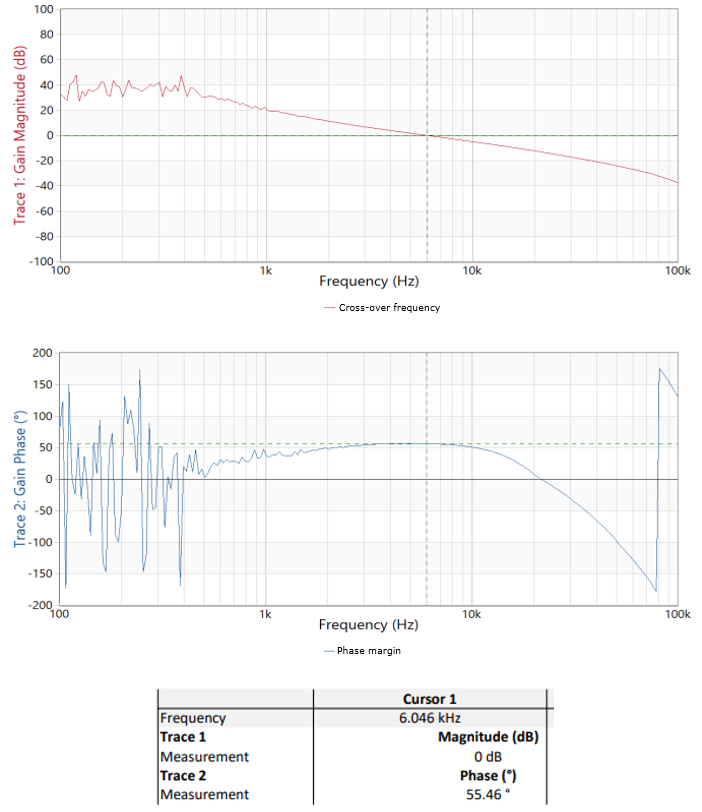
Bode plot and transient response
The Bode plot and transient response of one phase in voltage control mode is shown in
Figure 39
and
waveforms
stability of the buck peak current control mode is checked using an OMICRON Bode 100 device. The measured phase margin is about 55.46 degrees and the crossover frequency is 6.046 kHz.
For the setup of the Bode 100 network analyzer, see the OMICRON Bode 100 user manual and the PSOC™ Control Dual Buck Evaluation platform user guide.
Frequency analysis
Figure 39.
PCCM Bode plot
Waveforms
Figure 40.
Peak current control mode - variable load

The reference output voltage is 5 volts.
Figure 40
shows the output voltage waveform in maximum load condition. The output voltage is steady at 5 V with the PWM frequency of 300 kHz. The average inductor current is 1.185 A but the maximum inductor current is 1.39 A.
Figure 41.
Peak current control mode - transient load - overshoot
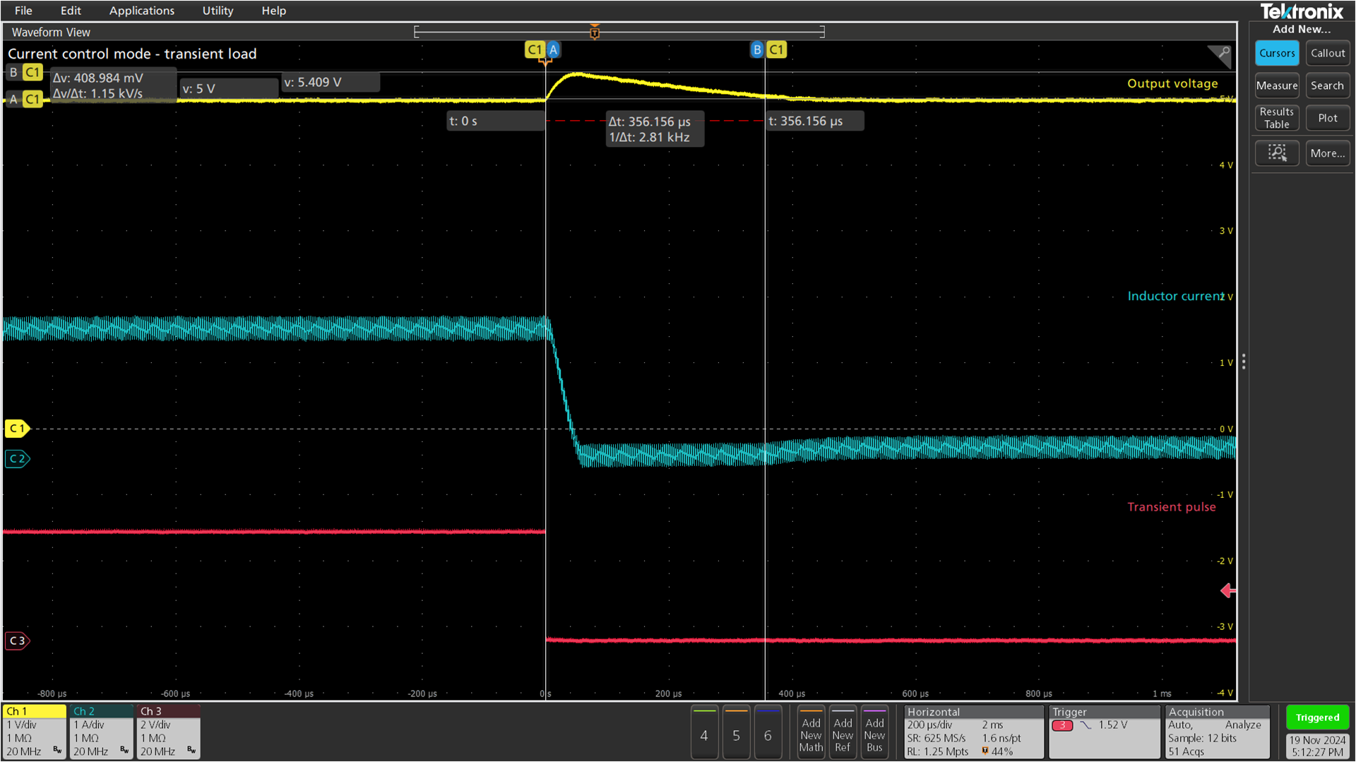
The output voltage waveform at a transient load condition (overshoot) is shown in the
Figure 41
. Due to the sudden change in load the overshoot in voltage is 408.984 mV and settling time is 356.156 μs.
Figure 42.
Peak current control mode - transient load - undershoot
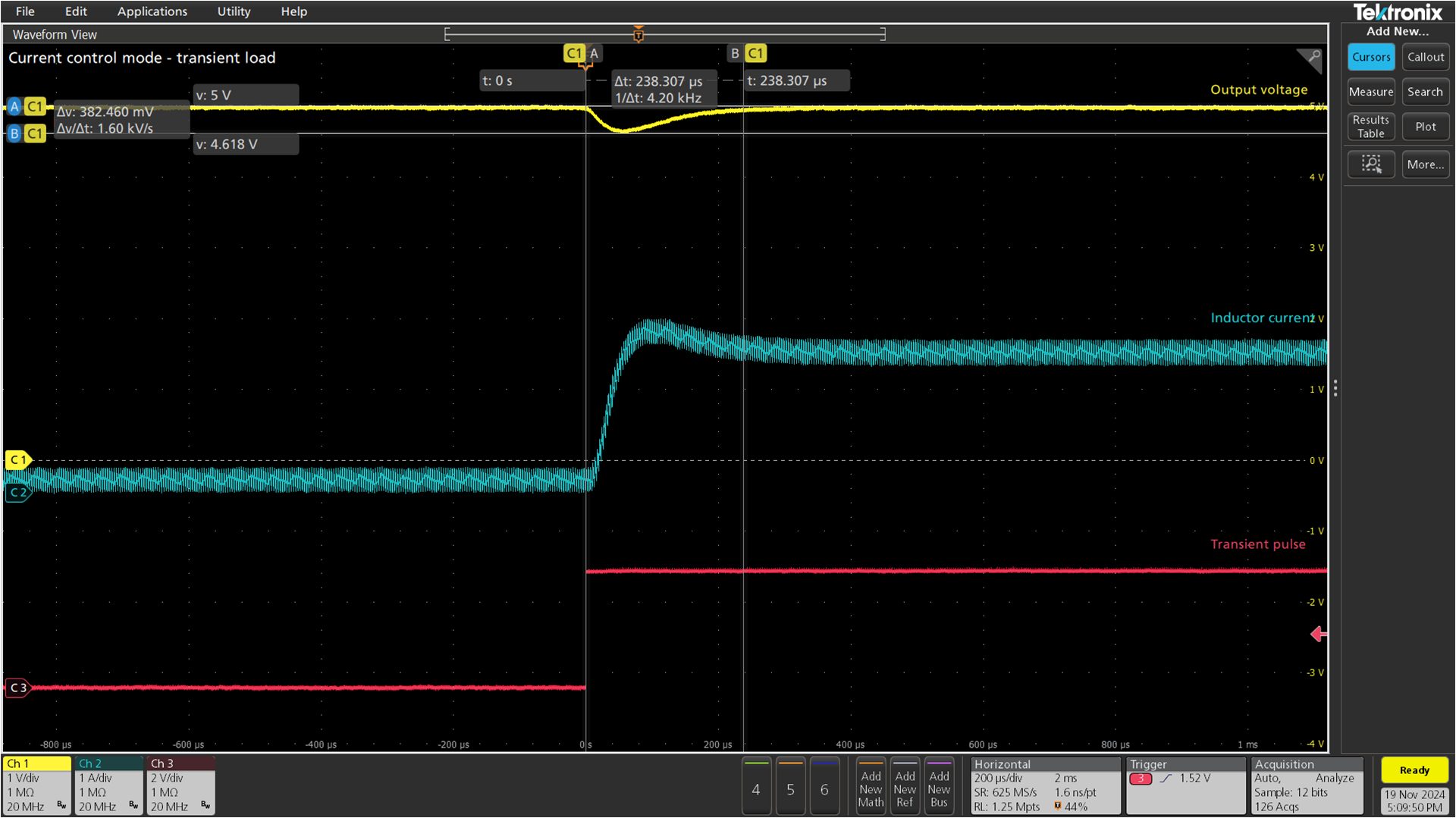
The output voltage waveform at a transient load condition is shown in the
Figure 42
. Due to the sudden change in load the overshoot in voltage is 382.460 mV and settling time is 238.307 μs.
Getting started with a power conversion code example
This section explains how to use the power conversion code examples available for PSOC™ Control C3 MCU in ModusToolbox™. It also explains the hardware setup, software setup, ModusToolbox™ project creation, and flashing/debugging the code.
Hardware setup
The configuration of the dual buck evaluation board to use the code example are discussed in the following section.
Hardware configuration
This section gives information about the header connections and load settings to use with the code examples.
The dual buck evaluation board integrates onboard transient load and linear load circuits, providing individual load control for each buck circuit, see
Figure 43
.
An SPDT switch, SW4 for Buck1 and SW5 for Buck2, provides an easy selection between the transient load and the linear DC load circuits, allowing for flexible load management.
Header J6 for Buck1 and J9 for Buck2 default to a short with a 24 Ω at 5 V output voltage, ensuring continuous conduction mode (CCM) for the buck regulator. Additionally, header J5 for Buck1 and J8 for Buck2 offer control to connect or disconnect the transient and linear load.
For higher buck output voltages, you must disconnect the onboard load from connectors J5, J6 for Buck1 and J8, J9 for Buck2, and make use of external load on connectors J7 for Buck1 and J10 for Buck2.
To use the dual buck evaluation board in multi-phase topology, short the J14 header. Keep the header J14 disconnected for all other loop topologies.
To use the buck converter solution using PCCM multi-instance code example, short header J5, J6 for Buck1 and J8, J9 for Buck2 keeping the header J14 disconnected.
Figure 43.
Load information
Note:
Do not switch from the transient load to variable load using SPDT switches when the converter is running. It will cause the converter to generate a fault signal. Only change it when the converter is in the OFF state.
Test points
To verify and analyze the performance and waveform, 39 test points are provided on the dual buck evaluation board. A few important test points are mentioned in
Table 14
.
Test point | Description |
|---|---|
TP23 | Buck1 output voltage (VOUT) |
TP27 | Buck2 output voltage (VOUT) |
TP5 | Buck1 line PWM |
TP7 | Buck1 complementary PWM |
TP14 | Buck2 line PWM |
TP16 | Buck2 complementary PWM |
TP21 | Buck1 transient load pulse |
TP25 | Buck2 transient load pulse |
For more information about the dual buck evaluation board, see the
kit user guide
.
Creating ModusToolbox project
Follow these steps to create the example project using ModusToolbox™.
Open Eclipse IDE for ModusToolbox™, create a workspace and select the
Launch
Figure 44.
Eclipse IDE launcher
Select
New Application
in the
Quick Panel
Figure 45.
Quick panel
Select
KIT_PSC3M5_CC1
from
PSOC™ Control BSPs
and click
Next >
Figure 46.
BSP selection
Select
PCCM buck converter multi-instance
within the Power conversion to create a PCCM multi-instance project for
KIT_PSC3M5_CC1
Figure 47.
Code example selection
The created project is shown in the
Figure 48
. The important files are highlighted. To launch the PCC tool, click on the
Power Conversion Configurator
. The generated code is available in the
bsps
folder.
Figure 48.
Example project
Example code for buck converter
Note:
This sample code implemented for understanding purpose only.
main.c file
See the
Code Listing 5
and
Code Listing 6
for sample code for the buck converter.
Code Listing 5
shows the
main.c
file. In this file, the initializing, enabling, and start functions are performed using middleware.
Code Listing 5
/*******************************************************************************
* Header files
*******************************************************************************/
#include "cy_pdl.h"
#include "buck_protection.h"
/*******************************************************************************
* Global variables
*******************************************************************************/
/* Interrupt configuration structure of soft start. */
cy_stc_sysint_t soft_start_irq_cfg =
{
.intrSrc = SOFT_START_COUNTER_IRQ,
.intrPriority = 2UL,
};

/* Variables for protection for converter 1. */
float32_t buck1_vout_adc_res          = 0;
float32_t buck1_iout_adc_res          = 0;
float32_t buck1_temp_adc_res          = 0;
float32_t vin_adc_res                 = 0;
float32_t buck1_vout_avg              = 0;
float32_t buck1_iout_avg              = 0;
float32_t buck1_temp_avg              = 0;
float32_t vin_avg                     = 0;
uint32_t buck1_enable_protection      = false;

/*******************************************************************************
* Function name: soft_start_intr_handler
*********************************************************************************
* Summary:
* This is the interrupt service routine (ISR) for the soft start counter interrupt.
* It will be executed only until the completion of the soft start. It gradually
* increases the reference values until reaching the calculated final reference
* values in converters.
*******************************************************************************/
void soft_start_intr_handler(void)
{
/* Clears soft start interrupt. */
Cy_TCPWM_ClearInterrupt(SOFT_START_COUNTER_HW, SOFT_START_COUNTER_NUM, CY_TCPWM_INT_ON_TC);

/* Increments the reference value for buck1 and buck2. */
BUCK1_ramp();

/* Stops the counter when both counters are reached the reference value. */
if(BUCK1_ctx.res >= BUCK1_ctx.targ)
{
 /* Disables soft start IRQ after the completion of soft start. */
 Cy_TCPWM_TriggerStopOrKill_Single(SOFT_START_COUNTER_HW, SOFT_START_COUNTER_NUM);
}
}

/*******************************************************************************
* Function name: hardware_init
*********************************************************************************
* Summary:
* This is the hardware peripheral initialization and enabling function.
* In this function all peripheral including TCPWM, HPPASS, and interrupt are configured.
*******************************************************************************/
void hardware_init(void)
{
cy_rslt_t result;

/* Initializes the timer for soft starting. */
result = Cy_TCPWM_Counter_Init(SOFT_START_COUNTER_HW, SOFT_START_COUNTER_NUM, &SOFT_START_COUNTER_config);
if (result != CY_RSLT_SUCCESS)
{
 CY_ASSERT(0);
}

/* Initializes the interrupt for a soft start. */
result = Cy_SysInt_Init(&soft_start_irq_cfg, soft_start_intr_handler);
if (result != CY_RSLT_SUCCESS)
{
 CY_ASSERT(0);
}

/* Clears all pending interrupts before configuring interrupts. */
NVIC_ClearPendingIRQ(soft_start_irq_cfg.intrSrc);

/* Enables all interrupts. */
NVIC_EnableIRQ(soft_start_irq_cfg.intrSrc);

/* Enables all timer channels. */
Cy_TCPWM_Counter_Enable(SOFT_START_COUNTER_HW, SOFT_START_COUNTER_NUM);
}

/*******************************************************************************
* Function name: main
********************************************************************************
* Summary:
* This is the main function of the code example. It performs the initialization
* and printing of the message.
*******************************************************************************/
int main(void)
{
cy_rslt_t result;

/* Initializes the device and board peripherals. */
result = cybsp_init();

/* Board init failed. Stop program execution. */
if (result != CY_RSLT_SUCCESS)
{
 CY_ASSERT(0);
}

/* Enables global interrupts. */
__enable_irq();

/* Initializes the peripherals. */
hardware_init();

/* Enables the buck converters. */
BUCK1_enable(); /* buck1 */

/* Starts the buck converters simultaneously. */
BUCK1_start();

/* Starts the soft start of the converter. */
Cy_TCPWM_TriggerStart_Single(SOFT_START_COUNTER_HW, SOFT_START_COUNTER_NUM);

for (;;)
{

}
}
/* [] END OF FILE */
buck_protection.h file:
This is a separate file used for safety purpose. In this, a pre-processor callback function is implemented in which the ADC values are read and moving average is performed on these values. If the averaged values is greater than the threshold values, the buck converter is disabled.
Code Listing 6
/*******************************************************************************
* Header Files
*******************************************************************************/
#ifndef BUCK_PROTECTION_H
#define BUCK_PROTECTION_H

#include "cybsp.h"

/*******************************************************************************
* Macros
*******************************************************************************/
/* Number of samples for averaging the parameters used for overload protection */
#define AVERAGING_SAMPLES     (8U)
/*******************************************************************************
* Global Variables
*******************************************************************************/
/* Variables used for Protection for converter 1*/ /* buck1 */
extern float32_t buck1_vout_adc_res;
extern float32_t buck1_iout_adc_res;
extern float32_t buck1_temp_adc_res;
extern float32_t vin_adc_res;
extern float32_t buck1_vout_avg;
extern float32_t buck1_iout_avg;
extern float32_t buck1_temp_avg;
extern float32_t vin_avg;
extern uint32_t buck1_enable_protection;

/*******************************************************************************
* Function Name: buck1_pre_process_callback
*********************************************************************************
* Summary:
* This is the callback from the buck1 ISR running the control loop. In this
* function, protection logic for buck1 is implemented.
*******************************************************************************/
__STATIC_INLINE void buck1_pre_process_callback(void)
{
/* Read result from ADC result register. */
buck1_vout_adc_res = BUCK1_Vout_get_result();
vin_adc_res        = BUCK1_Vin_get_result();
buck1_iout_adc_res = BUCK1_Iout_get_result();
buck1_temp_adc_res = BUCK1_Temp_get_result();

/*Moving Average calculation*/
buck1_vout_avg = (float32_t)((buck1_vout_avg - ((buck1_vout_avg - buck1_vout_adc_res) / AVERAGING_SAMPLES)));
buck1_iout_avg = (float32_t)((buck1_iout_avg - ((buck1_iout_avg - buck1_iout_adc_res) / AVERAGING_SAMPLES)));
buck1_temp_avg = (float32_t)((buck1_temp_avg - ((buck1_temp_avg - buck1_temp_adc_res) / AVERAGING_SAMPLES)));
vin_avg        = (float32_t)((vin_avg        - ((vin_avg        - vin_adc_res)        / AVERAGING_SAMPLES)));

/* Check if load protection is turned ON */
if (buck1_enable_protection == true)
{
 /* Check for under & over boundaries */
 if(((buck1_vout_avg < BUCK1_Vout_MIN) || (buck1_vout_avg > BUCK1_Vout_MAX)) ||
    ((buck1_iout_avg < BUCK1_Iout_MIN) || (buck1_iout_avg > BUCK1_Iout_MAX)) ||
    ((vin_avg        < BUCK1_Vin_MIN)  || (vin_avg        > BUCK1_Vin_MAX))  ||
     (buck1_temp_avg > BUCK1_Temp_MAX))
 {
     /* Disable the buck converter when protection condition passed. */
     BUCK1_disable();

     /* Turn OFF fault LED. */
     Cy_GPIO_Clr(FAULT_LED_PORT, FAULT_LED_NUM);
 }
}
/* Check if load protection can be turned ON */
else if (buck1_vout_avg > BUCK1.ctx->targ)
{
 buck1_enable_protection = true;
}
}

#endif  /* BUCK_PROTECTION_H */
/* [] END OF FILE */
The sample code uses multiple middleware functions as follows:
BUCK1_ramp()
: This is a function used for soft start purpose. The function is used in the timer's interrupt service routine. This function is gradually increasing the reference value until the final calculated reference value of the controlled parameter. The duration of the soft start is configured in the controller tab of the PCC tool
BUCK1_enable()
: This function is used for enabling the buck converter
BUCK1_start()
: This function is used for starting the buck converter
BUCK1_disable()
: This function is used for disabling the buck converter
BUCK1_Vout_get_result()
: This function is used to read output voltage value
BUCK1_Vin_get_result()
: This function is used to read input voltage value
BUCK1_Iout_get_result()
: This function is used to read output current value
BUCK1_Temp_get_result()
: This function is used to read temperature value
The threshold values in the sample code is configured in the PCC tool and an equivalent variable is generated by the middleware
A detailed state machine is implemented in the released code example which explores all the features of the kit, middleware, and PCC tool. For more information, see the
middleware
and
PCC tool
documentation.
Summary
This application note explored the synchronous buck converters, the PSOC™ Control C3 MCU device architecture, associated development tools, and buck converter implementation using the PSOC™ Control C3 MCU and PCC tool. The PSOC™ Control C3 MCU is a truly programmable embedded system-on-chip with configurable analog and digital peripheral functions, memory, and a powerful processor on a chip. The integrated features and low power modes make the PSOC™ Control C3 MCU an ideal choice for the power conversion and motor control solutions.
References
For a complete and up-to-date list of PSOC™ Control C3 MCU code examples, see
Infineon GitHub page
. For additional PSOC™ Control C3 MCU-related documents, see the
PSOC™ Control C3 MCU
webpage.
For power conversion application documents, see
PSOC™ Control C3P
For motor control applications documents, see
PSOC™ Control C3M
For dual buck evaluation kit information, see
KIT_PSC3M5_DP1
002-39715: KIT_PSC3M5_CC1 PSOC™ Control C3M5 Digital Power Control Card user guide
002-39714: KIT_PSC3M5_DP1 PSOC™ Control C3M5 Complete System Dual Buck Evaluation Kit user guide
AN238329 - Getting started with PSOC™ Control C3 MCU on ModusToolbox™ software
Middleware documents on
GitHub
PCC tool
user guide
ModusToolbox™ Industrial MCU Pack
OMICRON Bode 100 quick start guide
Glossary
This section lists the most commonly used terms that you might encounter while working with PSOC™ Control MCUs.
Board support package (BSP):
A BSP is the layer of firmware containing board-specific drivers and other functions. The board support package is a set of libraries that provide firmware APIs to initialize the board and provide access to board level peripherals
Personality:
A personality expresses the configurability of a resource for a functionality. For example, the SCB resource can be configured to be an UART, SPI, or I2C personalities
Middleware:
Middleware is a set of firmware modules that provide specific capabilities to an application. Some middleware may provide network protocols (e.g., CAN FD), and some may provide high-level software interfaces to device features (e.g., TCPWM, HPPASS)
ModusToolbox™
: An Eclipse-based embedded design platform for embedded systems designers that provides a single, coherent, and familiar design experience, combining the industry’s most deployed Wi-Fi and Bluetooth® technologies, and the lowest power, most flexible MCUs with best-in-class sensing
Peripheral Driver Library (PDL):
The PDL simplifies software development for the PSOC™ Control C3 MCU architecture. The PDL reduces the need to understand register usage and bit structures, so easing software development for the extensive set of peripherals available
Revision history
Document revision | Date | Description of changes |
|---|---|---|
** | 2024-12-06 | Initial release |
Trademarks
The Bluetooth® word mark and logos are registered trademarks owned by Bluetooth SIG, Inc., and any use of such marks by Infineon is under license.