AN240106 Getting started with PSOC™ Control C3 security
About this document
This application note provides information on how to get started with security on the PSOC™ Control C3 MCU out of the box. It contains guidance on how to provision and program a secure application. It introduces the security architecture of the PSOC™ Control MCU, consisting of an Arm® Trust Zone-enabled Cortex®-M33. This document provides a brief overview of the security features available on the device.
Intended audience
This document is intended for customers who want to start with enabling secured boot and explore security feature implementation on PSOC™ Control MCU devices.
Overview of PSOC™ Control C3 MCU
The PSOC™ Control C3 MCU is a single core device that contains Arm® TrustZone enabled Cortex® M33, SONOS flash, a range of peripherals, including high-performance programmable analog subsystem (HPPASS), coordinate rotation digital computer (CORDIC), ADC, UART, SPI, I2C, CAN FD, crypto accelerators, and several other blocks. The CM33 allows for both a secure programming environment (SPE) and a non-secure programming environment (NSPE). Although a single CPU is used, individual SPE and NSPE projects can be created. The BootROM is responsible for the initial secure boot and the root of trust (RoT). The main function of the BootROM is to configure the system information, authenticate the application, and transfer control to the application.
Figure 1
shows the basic hardware cores and boot flow of the PSOC™ Control C3 MCU.
Figure 1.
Basic hardware blocks and boot flow
Sl. No. | Security features | Comments |
|---|---|---|
1 | Secure boot | The chain of trust includes up to the first Original Equipment Manufacturer (OEM) code. The policy file parameter determines if secure boot is extended to the first OEM code. |
2 | Secured debug | Yes. supported |
3 | Secured firmware upgrade | Yes, BootROM supports an in-built device firmware update (DFU) serial interface |
4 | OEM policies | Yes, supported |
5 | Transition to production LCS | Yes |
6 | Transition to RMA LCS | Yes, with authentication |
7 | OpenRMA with debug token | Yes, and signed by Infineon |
8 | OEM RoT keys (pub keys) | Yes, it supports initial and alternate keys in case of key revocation is required |
Ease of development
Device lifecycle stages (LCS)
Devices are shipped in the development stage, which allows the device to be provisioned and programmed as many times as needed to develop the final application. Devices are shipped with a default policy that defines all debug ports as open and allow application execution without code authorization. This allows you to program, evaluate, and debug the parts prior to any knowledge about security or code signing.
During the development stage, the OEM can take ownership of the part, allowing it to replace the default policy file with a custom policy. All aspects of the production stage can be simulated, including locking down the CPU access ports, which will lock out any attempt to connect the debugger to the part. The only difference between the development and production stages from a code operation point of view is that the SYS_AP (system access port) cannot be disabled in the development stage. This ensures that the developer cannot be locked out of the part and can, at any time, recover from a device configuration error and even return the device to its original state. When the firmware is ready for production, the device can be advanced to the production stage.
The production stage locks down the device owner, meaning that the key used to authenticate the firmware can no longer be changed from what was programmed into the device. The debug ports, including SYS_AP, can all be disabled or left enabled as per your requirement. Devices can be advanced to the production stage after receiving them from Infineon. This is the typical model once the OEM starts to ship their product. There is no need to transfer ownership in the development stage; instead, you can take ownership and advance the device to the production stage in a single step as part of provisioning the device.
The RMA stage is only used in the event that a problem is found in the hardware and the device must be shipped back to Infineon for failure analysis (FA).
Figure 2
shows the flow from development to RMA.
Note: Blowing eFuses to change LCS requires VDDIO0 to be 2.5 V. See the datasheet for more details.
BootROM execution flow depends on the lifecycle stage at which the MCU is running. LCS is dictated by blowing eFuse bit values in to the device. During provisioning, the LCS can be moved for the device. Infineon signed RAM applications are used to provision the assets into the device and change the device LCS. RAM applications and the associated input parameters are loaded into the device SRAM through a SWD or DFU serial interface. RAM applications are authenticated by BootROM before it execute from device SRAM. The LCS is sequential and cannot be reverted back to the previous stage, since the LCS is maintained in the eFuse memory. Device DAP access restriction shall be based on a deployed policy, which will be applicable for both production and development LCS.
Figure 2
shows the LCS transition in the PSOC™ Control C3 device.
Figure 2.
LCS transition
Development LCS
Device shipped to customer in development LCS by default
OEM policy assets will be provisioned in this LCS
Transition allowed in this stage is production or RMA
cyapp_prov_oem RAM application will be used to do the device LCS transition from development to production
Device can be provisioned again until the prov_oem_complete parameter is false. See the
policy_oem_provisioning.json
file
Production LCS
This is a lifecycle stage of a secured device
OEM policy assets (example, SECURE_HASH) will be provisioned prior moving to this LCS
Device will launch the customer application only when authentication is success
Production LCS is mandated for a secured device and it protects the customer application from tampering
The only transition allowed in this stage is production to RMA LCS
After the device transition to production LCS, the protection state is set to SECURE
RMA LCS
RMA LCS allows Infineon to do failure analysis (FA)
For FA, customer transitions the device LCS to RMA and ship the device to Infineon
RMA transition is allowed only when the device is in production LCS
RMA transition in production LCS requires a certificate signed with the OEM_ROT_KEY
cyapp_to_rma RMA application will be used to transition the device in to RMA LCS
During the RMA transition, the following list of assets will be cleared from the device
HUK
IAK
MPN_KEY and MPN_ROT_KEY_01_HASH
OEM policies
All user flash contents
PROT_FW policy
Infineon policies
After the device moved to RMA state, the device will not boot the OEM application
Boot policy update
Boot policy is one of the input parameters for the RAM application, which is used to provision the device
The RAM applications are signed by Infineon and the input parameters are not, but it is bundled as a downloadable module (DLM) packet using a provisioning tool
The RAM application bundle can be sent to the device SRAM location via DFU serial interface or SWD using the Edge Protect Tools
Note: Edge Protect Tools support only SWD or DFU serial interface (UART, I2C, SPI) for provisioning the device
These SWD/ DFU ports are invoked by a provisioning tool
Note:
BootROM has a built-in DFU-supported serial interface to receive RAM application
After the RAM application is moved to SRAM, the BootROM authenticates the RAM application and gives control to the RAM application
Further, the RAM application will provision the device. At the end of the RAM application, the device will go reset and the BootROM will execute/branch based on the boot policy configured
Figure 3.
Boot policy update
Development flow
The typical development flow for a PSOC™ Control C3 device is the same work flow as most other systems.
Provision the device
Design, develop, and modify the project code
Compile/link
Program the device
Run/debug on the device
Getting started
Infineon ships the device with development LCS and provisioned with BOOT_SIMPLE_APP configuration, which the BootROM can expect the first user application to be in raw format and launches the application without authentication.
General application development instructions are available in the Application development instructions section of the
Getting started with PSOC™ Control C3 MCU on ModusToolbox™ software
document. Once you are ready to provision the device with a secure boot configuration, do the following:
Initialize application directory
Generate two key pairs (private/public optional)
Edit policy file
Provision the device
Infineon’s Edge Protect Tools is a set of command-line tools used to perform the needed functions for key signing, key generation, provisioning the device, and so on. These tools are executed from inside a shell tool. It is recommended to use the modus-shell, which is installed along with Edge Protect Suite. Before using these tools, change the directory to the top level of your application folder, the same level as the application project directories.
Note:
Ensure that the KitProg3/MiniProg4 on your PSOC™ Control C3 device is updated to firmware version 2.60.1412 or later.
For more information about the KitProg3, see the
Getting started with PSOC™ Control C3 MCU on ModusToolbox™ software
document.
Initialize the application directory
When initializing the application folder for using Infineon’s
Edge Protect Tools
, several folders will be created in your application directory. The following is a list of these folders and their contents.
keys:
Any keys that you create with the Edge Protect Tools will be placed in this directory. If you prefer to create your own keys, you must place the keys in this directory
logs:
Each time you run the Edge Protect Tools, creates a time and date log files. These files can assist in debugging any problems with the tools that can occur. This directory is created for the first time that you execute an Edge Protect Tools command after initialization
packets:
Some commands generate JSON-formatted packets that are downloaded into the device or will be used by another command. These files are placed in this folder
policy:
Contains some sample policy files that can be modified or copied as required. Eventually, each one will have a custom policy file that fits their application
The following command will initialize the application directory and prepare it for all the following Edge Protect Tools commands, it will be executed once per application.
edgeprotecttools -t psoc_c3 init
Execute the following command once per session to configure the connection between the tool and a MiniProg4 or kit SWD port.
edgeprotecttools
set
-ocd --name openocd --
path
<openocd_path>
Replace
<openocd_path>
with the path to the openocd directory installed when the Early Access Pack is installed. Typically, will be in the
C:/Users/username/ModusToolbox/packs/ModusToolbox-PSOC-C3-Early-Access-Pack/tools/openocd
. Replace the username with the equivalent on your system.
Note:
If you are using modus-shell on a macOS system, the recommended usage for EdgeProtectTool is as follows:
arch -arm64 edgeprotecttools <command>
Key generation
You need to create two key pairs that are private and public keys. The second key pair is useful if you need to revoke the first key due to a private key security breach. The following two commands generate two keys that will be placed in the key's directory.
edgeprotecttools create-key --key-type ECDSA-P256 --output keys/oem_private_key_0.pem keys/oem_public_key_0.pems
edgeprotecttools create-key --key-type ECDSA-P256 --output keys/oem_private_key_0.pem keys/oem_public_key_0.pem
The keys generated are 256-bit ECC keys and the output is in the .pem format. This is a common ASCII format compatible with many public-domain tools.
Application structure
This section shows a typical folder structure for an application. The term "application" refers to one or more projects that run on this CPU. Although the CM33 is a single CPU, it includes TrustZone, so there will be two projects associated with it as follows:
A Secure Processing Environment (SPE)
Non-Secure Processing Environment (NSPE) project
It is an option to support NSPE project if required. Each application can contain four additional folders that are generated when the Edge Protect Tools that are used to initialize the application for provisioning. These folders include:
policy
keys
packets
logs
They contain the default policy files, the generated or stored keys, packets generated by the tools, and log files generated each time you execute the Edge Protect Tools. See the Getting started for more details about Edge Protect Tools and these folders.
Figure 4.
File structure
Basic application structure
In the default application structure, only one SPE project will be created and presented, this default structure can be used if you need only an SPE-based project, see
Figure 4
(a). Additionally, you can add an NSPE project if needed, see
Figure 4
(b).
The first application will be authenticated by BootROM and the application must be signed if the boot configuration is BOOT_ONE_SLOT, BOOT_TWO_SLOTS, BOOT_THREE_SLOTS, and BOOT_IDLE configurations. Signing the first application is a mandate for production LCS.
If the Edge Protect Bootloader (EPB) is used, it will be viewed as a separate application within ModusToolbox™ 3.3 and it will be compiled, linked, and programmed separately from the main application, see
Figure 4
(c). The main application will contain the CM33 SPE and CM33 NSPE project. Note that in this configuration, only the EPB application directory includes the four folders required when provisioning the device. This is because when the device boots up, the secure boot sequence only extends the chain of trust to the next application. In this case, the next application is the EPB. EPB is responsible for extending the chain of trust to the next application by authenticating the code. Provisioning and the policy file only directly affect the first OEM application that is the EPB. Keys used to authenticate the main application can have been loaded into the device during provisioning or can be stored in the EPB; this is up to you and the application requirements.
Boot flow
BootROM executes the code from the beginning of power-on reset (POR) until the launch of an OEM application. The main functionality of BootROM is to authenticate and launch the next stage application. BootROM consists of ROM_BOOT and FLASH_BOOT.
Boot sequence
After reset, the ROM_BOOT applies basic trim, configures clocks, and validates the SFLASH
ROM_BOOT execution jumps to FLASH_BOOT on successful validation
FLASH_BOOT authenticates the next stage application (OEM)
FLASH_BOOT prepares to launch the application on successful authentication
If authentication fails, the device will go to the DEAD branch
shows the steps involved in the BootROM root of trust.
Figure 5.
Root of trust
shows the elements used to validate each stage of BootROM validation.
Step | Element | Checked by | Using |
|---|---|---|---|
1 | ROM | N/A immutable | N/A immutable |
2 | ASSET_HASH | ROM_BOOT | eFUSE zeroes |
3 | SFLASH_BOOT code | ROM_BOOT | ASSET_HASH |
4 | OEM_ROT_KEY | SFLASH_BOOT code | eFUSE_HASH |
5 | OEM Application | SFLASH_BOOT code | OEM_ROT_KEY |
The device internal user flash region can have multiple images based on the BOOT_CFG_ID parameter present in the boot policy. The boot policy will be configured during device provisioning.
BOOT_CONFIG_ID parameter will have the following allowed configuration.
BOOT_SIMPLE_APP
BOOT_ONE_SLOT
BOOT_TWO_SLOTS
BOOT_THREE_SLOTS
BOOT_IDLE
BOOT_SIMPLE_APP
Simple OEM application is a default BootROM configuration
One OEM application will be present in the user flash region with basic application format (interrupt table and code, no MCUboot format)
OEM application start address is the start of internal flash
BootROM will not authenticate the OEM application in this configuration
Figure 6.
Boot simple app
Secure boot
The process of verifying and validating the integrity and authenticity of firmware as a prerequisite to their execution. At each stage of the boot process checks that code is authorized to run before execution.
PSOC™ Control C3 BootROM authenticates user application based on boot configuration.
boot_cfg_id | Description |
|---|---|
BOOT_ONE_SLOT | BootROM authenticates the first OEM application present in the use flash. |
BOOT_TWO_SLOTS | BootROM authenticates the two (primary, staging) OEM application present in the use flash and launch the primary application. |
BOOT_THREE_SLOTS | BootROM authenticates the three OEM application present in the use flash and launch the first OEM application. |
BOOT_ONE_SLOT
One OEM application can be present in the user flash region with the MCUboot format
BOOT_APP_LAYOUT[0] contains start address and size for the application
BootROM will authenticate and launch the OEM application
Figure 7.
Boot one slot
BOOT_TWO_SLOTS
Two OEM applications can be present in the user flash region
BOOT_APP_LAYOUT[0 to 1] contain the start address and size for the primary and secondary/staging images
Primary slot is for boot and the secondary slot is for update the image
BootROM will authenticate a secondary image and update it in to the primary slot on successful authentication
Further BootROM launches OEM application from primary location
Figure 8.
Boot two slots
BOOT_THREE_SLOTS
Three OEM applications can be present in the user flash region
BOOT_APP_LAYOUT[0 to 2] contain the start address and size correspondingly for the first application (Example: TF-M) application, second application (OEM App) primary slot, and secondary slot
Here the first application can be either TF-M software or EdgeProtectBootloader based OEM bootloader or protected firmware
Using the multi-image authentication feature, the BootROM will authenticate each stage of the application and launch the primary image
If the first image is invalid or both of the primary and secondary images are invalid, the device will go to dead branch
Figure 9.
Boot three slots
Dual bank application
The user flash regions can be split into two equal regions. Both regions will have dual bank counter offset and an OEM application
BootROM can read the dual bank counter offset value and identify the active bank region
BootROM will then authenticate the active bank region and execute the application
Figure 10.
Dual bank configuration
Code signing and verification
Code signing and verification must for secure boot configuration. In other words, the user application must be signed for BOOT_ONE_SLOT, BOOT_TWO_SLOTS, and BOOT_THREE_SLOTS configurations.
Code signing
To verify the user application, create a digital signature and append it to the end of the project binary during build time. The user code is not encrypted, but the digital signature is the encrypted digest one. The digital signature is generated by encrypting the digest with the ECDSA private key. In this case, it is the OEM_ROT_PRIVATE_KEY. The digest is generated by running the user project binary through an SHA-256 hash function. This method guarantees that a third party without access to the OEM’s private key cannot properly sign the application code, which is therefore only created and signed by the OEM.
Note:
The MCUboot-based Project Header consists of image attributes and Project Trailer consists of image trailer TLV information.
Figure 11.
Code signing
Code validation
When secured boot is enabled through provisioning, whether the device is in production or development LCS, the BootROM must verify the OEM code prior to execution. The project binary image must be signed by the OEM_ROT_PRIVATE_KEY before loaded into the device. BootROM verifies the OEM code by first calculating the hash of the project binary image. It then uses the calculated hash, the project digital signature that is appended to the end of the code, and the OEM_ROT_PUBLIC_KEY to verify if the OEM code is authentic. If the code fails verification, the BootROM will not jump to the user code but will wait in an endless loop until the device has been reset.
Figure 12
shows a graphical representation of this process.
Figure 12.
ECDSA code verification
Edge Protect Tools
Overview
Edge Protect Tools is a comprehensive security tools package built on Python, offering a command-line interface to interact with MCUs for various purposes. These purposes include: provisioning, device integrity checks, RMA transition, and more. The tools are developed using the Python programming language and leverage several third-party Python modules to handle different tasks. For instance, these modules are used to manage configuration files in JSON format, object files in ELF format, and perform cryptographic operations.
Use any shell command-line tool to interact with Edge Protect Tools. However, Infineon recommends using modus-shell, which comes bundled with the ModusToolbox™ installation package for a seamless interaction experience. When executing commands that require interaction with the MCU, such as provisioning, the tools prepare the necessary provisioning packets and communicate with the device using programming tools like OpenOCD via the SWD interface or the DFU Host Tool via serial interfaces like I2C, SPI, and UART.
Figure 13
shows the provisioning flow between OEM and MCU through Edge Protect Tool (EPT).
Figure 13.
PSOC™ Control C3 MCU provisioning flow
The Edge Protect Tools package supports a range of operations that cater to various security-related needs. Some of the key operations supported by the tools include:
Provisioning, which involves injecting keys and policy into the device, ensuring a secure setup
Re-provisioning allows for modifying certain configurations post-provisioning and providing flexibility in device management
Enables a Device Integrity Exam, which verifies the authenticity of the device and ensures it is in a known state, thereby preventing any potential security breaches
In addition, the Edge Protect Tools facilitate key pair generation, creating key pairs that can be utilized for provisioning, and image signing purposes. Certificate generation is another supported operation, which generates certificates that can be used for debugging and RMA transition
The tools support signing images with the OEM key, ensuring the integrity and authenticity of the images used in the device
Figure 14.
Edge Protect Tools design flow
Device communication
The Edge Protect Tools package supports communication with the device using programming tools such as the OpenOCD tool via the SWD interface on the device, or by utilizing the DFU Host Tool via serial interfaces like I2C, SPI, UART, or USB. The Edge Protect Tools package does not directly call the programming tool commands, but instead utilizes a wrapper mechanism to interface with the programming tools. This model has the potential to be further extendible to other programming tools, although this is currently outside the scope of the tool's current version.
Packaged assets
OEM policy - The OEM policy (
policy_oem_provisioning.json
) file can be used to configure the device policy configurations, which is located in the policy folder as part of the Edge Protect Tools package.
Edge Protect Tools package for PSOC™ Control C3
The Edge Protect Tools is packaged as a part of the Edge Protect Security Suite for the PSOC™ Control C3 device. Follow these steps to setup Edge Protect Security Suite.
Download and install the Infineon Developer Center Launcher
Login using your Infineon credentials
Download and install the “ModusToolbox™ Edge Protect Security Suite” from Developer Center Launcher
Note:
The default installation directory of the Edge Protect Security Suite in Windows operating system is
C:/Users/
<USER>
/Infineon/Tools
. After installing the Edge Protect Security Suite, add the Edge protect tools executable to system PATH variable (
/ModusToolbox-Edge-Protect-Security-Suite-
<version>
/tools/edgeprotecttools/bin
)
To utilize the executable file, find the executable file in the
./bin
directory, which is compatible with Windows, Linux, and macOS. To use it directly, add the executable path to your system's environment variable PATH.
Note:
You need to install Python separately. The Edge Protect Tools support Python versions ranging from 3.8 to 3.12.
Once you have installed the Edge Protect Tools package, initialize it for a specific target device. For example, to initialize it for the PSOC™ Control C3 device, navigate to your working directory and execute the following command in a shell CLI:
edgeprotecttools.exe -t psoc_c3 init
After that, set up the OpenOCD path to be used by the tools. Run the following command:
edgeprotecttools.exe set-ocd --name openocd --path <openocd path>
replacing <openocd path> with the actual path to the OpenOCD tool on your system. After initialization, a specific folder structure will be created in your working directory.
To provision the device, execute a specific command using the Edge Protect Tools utility. The basic command is as follows:
edgeprotecttools -t psoc_c3 provision-device -p policy/policy_oem_provisioning.json
However, if you are using an external MiniProg, specify the probe ID in the command. To find the probe ID, run the following command:
~/ModusToolbox/tools_
3.3
/fw-loader/bin/fw-loader.exe --device-list
This will provide you with a connected device, including their respective probe IDs. If you have multiple MiniProgs connected to your system, specify the correct probe ID in the provision-device command. For example,
edgeprotecttools -t psoc_c3 provision-device -p policy/policy_oem_provisioning.json --probe-id
061003
B803260400
If you want to lock in the policy parameters and prevent any further modifications to the configuration, you can set the
prov_oem_complete
parameter to
true
in the
policy_oem_provisioning.json
file and provision the device. Once this parameter is set to true, the device is essentially "locked" and cannot be provisioned again in normal provisioned LCS. This ensures that the configured policy parameters remain unchanged and secure.
Code Listing 6
"prov_oem_complete": {
"description": "Indicates OEM assets are finalized in SFLASH",
"warning": "Once the 'prov_oem_complete' parameter value is set to true, it cannot be changed! No further updates to SFLASH are allowed",
"value": true
},
To transition a device to the production LCS, set the
target_lcs
parameter to
SECURE
and provision the device. Once the device is moved to the secure LCS, it is locked into this stage and cannot be provisioned again. Additionally, it is mandatory that the user application be in MCUboot format, as the device will only launch authenticated applications during the secure LCS. This ensures that only trusted and verified applications can run on the device.
Code Listing 7
     "device_policy": {
  "target_lcs": {
  "description": "The LCS to which the transition should be done",
  "applicable_conf": "NORMAL_PROVISIONED, SECURE",
  "value": "SECURE"
  },
     }
Note:
The terms NORMAL_PROVISIONED LCS and DEVELOPMENT LCS are interchangeable, and similarly, SECURE LCS is equivalent to PRODUCTION LCS. The key distinction between DEVELOPMENT LCS and PRODUCTION LCS remain in the requirement for secure boot. In DEVELOPMENT LCS, secure boot is not mandatory, whereas in PRODUCTION LCS, secure boot is a requirement.
Processing, memory, and peripheral isolation
The Cortex® M33 CPU of PSOC™ Control C3 MCU has the Arm® TrustZone-M security extension enabled. The extension allows partitioning of the system's resources into two worlds: Secure and Non-secure. Additionally, the extension introduces Secure and Non-secure states to the CPU. In the Secure state, the CPU has access to all the resources on the MCU while in the Non-secure state the CPU has access only to the Non-secure resources. The TrustZone extension adds new access restrictions which isolates resources into Secure and Non-secure worlds at the hardware level.
The TrustZone-M security extension enables you to create an isolated execution environment and execute Secure and Non-secure software on the same M33 CPU. Since the Secure and Non-secure worlds are isolated at a hardware level, there is no information leakage from Secure to Non-secure software. Typically the software, such as bootloader, cryptography service, secure storage service, etc. are executed in the Secure world. The Non-secure software handle communication with the external world and other user tasks. If the Non-secure software requires some service from Secure software, the TrustZone allows it to create Secure entry points to call Secure software from Non-secure software.
The isolation provided by TrustZone is address space based. The memory and peripherals are aliased into two regions in the address space, i.e., same memory/peripheral is mapped in multiple regions in the 4 GB address space. The aliasing is done using the bit 28 of the address. If bit 28 = 0, the address is Non-secure and if bit 28 = 1, the address is Secure. The CPU in Secure state must use the Secure alias for code execution and peripheral access, while in Non-secure state, the CPU must use the Non-secure alias.
Table 4
shows how the 256 KB flash, 64 KB RAM, and peripherals of the MCU are mapped to multiple address ranges.
Memory/peripheral | Address range | Alias |
|---|---|---|
Flash | 0x0200_0000 -0x0203_FFFF / 0x2200_0000 - 0x2203_FFFF | Non-secure |
0x1200_0000 - 0x1203_FFFF / 0x3200_0000 - 0x3203_FFFF | Secure | |
RAM | 0x0400_0000 - 0x0400_FFFF / 0x2400_0000 - 0x24200_FFFF | Non-secure |
0x1400_0000 - 0x1400_FFFF / 0x3400_0000 - 0x3400_FFFF | Secure | |
Peripherals | 0x4200_0000 - 0x43FF_FFFF | Non-secure |
0x5200_0000 - 0x53FF_FFFF | Secure |
On top of TrustZone, protection context (PC) is implemented in PSOC™ Control C3 MCU for additional security. Protection context is a protection mechanism, which provides the ability to restrict memory and peripheral resources between multiple masters or from the same master executing multiple applications. Protection context adds an additional attribute to bus masters on top of the Non-Secure (NS) and Privilege attribute. This additional attribute is used for isolating resources by memory protection controller (MPC) and peripheral protection controller (PPC).
After reset, the M33 CPU starts in Secure state and the BootROM executes in Secure state. The BootROM later transfers the control to the user application. The BootROM does not change the CPU state. The CPU continues to run in a Secure state, therefore, it is required that the first user application must be a Secure application. Depending on the use case, you can build the entire application as Secure software or it can be split into Secure and Non-secure software. If the application is split into Secure and Non-secure software, then ensure that the memory and peripherals are partitioned such that the Non-secure software has access to its resources. The next section describes how the memory is partitioned to enable Non-secure software execution.
Note:
The majority of the code example for PSOC™ Control C3 are demonstrated as "secure software".
See the "TrustZone" and "Protection units" sections from
PSOC™ Control C3 architecture reference manual
for more information about TrustZone and protection context and its isolation capabilities.
Memory isolation
Memory isolation (partitioning) in PSOC™ C3 MCU is controlled with implementation-defined attribution unit (IDAU), secure attribution unit (SAU), and memory protection controller (MPC). The memory can be partitioned into Secure, Non-secure, or Non-secure callable (NSC: A special type of Secure region is used for calling Secure software from Non-secure software) regions by configuring these protection units.
IDAU:
It provides a fixed (non-configurable) implementation to indicate whether an address is Secure or Non-secure. It indicates an address as Secure if the 28th bit of address is '1' else, it is marked as Non-secure. The security attribute indication by IDAU is aligned with the address aliasing scheme shown in
Table 4
.
SAU:
It has eight programmable regions to indicate certain address ranges as Secure, Non-secure, or Non-secure callable. CMSIS provides the necessary assets (APIs and device headers) required to program SAU. SAU and IDAU are implemented as part of TrustZone extension and the attribution units work together to indicate whether an address is Secure or Non-secure, the higher security among the two is used as indication.
MPC:
It divides the flash and SRAM on to smaller blocks of 2 KB and configures Non-secure (NS), Read (R), and Write (W) attributes of each memory block for each protection context. If a memory block is marked as Secure, then it can be accessed by Secure alias address and if a memory block is marked as Non-secure, it can be accessed using Non-secure alias address. MPC configuration is stored in the MCU during the device provisioning process through the OEM policy.
The BootROM reads the OEM policy during device initialization and configures the SAU and MPC. After device initialization, the MPC configuration cannot be updated in the run time, the device must be re-provisioned to change it. SAU can be reconfigured in run time by Secure privileged software. Ensure that SAU and MPC configuration are aligned, that is they mark the same set of address range as Secure or Non-secure. In case of conflicting configuration, the program execution can end up in fault.
Depending on the application's needs, you can choose the isolation level required between Secure and Non-secure software. You can either rely only on TrustZone or use the additional isolation capability of protection context on top of TrustZone. If the context switching latency between Non-secure and Secure is critical, then it is recommended to use TrustZone isolation, as the protection context switching adds an additional overhead, which cannot be desired in certain applications. If security is the utmost priority, then use the additional protection context isolation.
Taking an example to demonstrate how the device memory can be partitioned by configuring SAU and MPC. Assume that a use case requires both Secure (PC2) and Non-secure (PC3) projects and the memory requirements for this application are as shown in
Figure 15
.
Figure 15.
Example memory partitioning
By default, TrustZone marks the entire memory as secure. SAU registers must be programmed with CMSIS to configure Non-secure and Non-secure callable regions. On Arm® TrustZone technology, see the
Armv8-M architecture reference manual
and see how SAU registers are configured to create Non-secure and Non-secure callable regions.
This section focuses on how to configure MPC memory access restrictions via the OEM policy.
Secure memory:
Secure memory uses Secure software in the Secure alias range. Out of reset, all the memory is marked as Secure with read/write access for all PCs that is Non-secure access to the memory is not allowed. Therefore, it is not required to configure the Secure regions in the OEM policy. Non-secure callable region is a type of Secure region and should be treated as Secure region in the MPC configuration. Optionally, you can restrict the Secure access to the memory to PC0-2. To enforce such restrictions, specify the NS, R, and W attributes for each PC. MPC configuration objects must be populated in
mpc_struct_ram
and
mpc_struct_flash
in the OEM policy to configure MPC.
The following objects show how the earlier mentioned memory access restriction can be implemented to configure secure memory regions in SRAM and flash respectively.
Code Listing 1
{
"description": "SRAM MPC configuration for secure region. Offset and size in KB. The values must be multiple of 2 (e.g. 0 KB, 2 KB, 4 KB, 8 KB, ...)",
"offset": "0 KB",
"size": "16 KB",
"attr": {
"description": "The MPC attributes for this memory region",
"comment_1": "WRN allow write, read, and NS only access",
"comment_2": "-RN allow read, NS-only access",
"comment_3": "--- and --N, no access",
"comment_4": "WR- read and write access, but NS=0 only",
"value": {
"pc0": "WR-",
"pc1": "WR-",
"pc2": "WR-",
"pc3": "---",
"pc4": "---",
"pc5": "---",
"pc6": "---",
"pc7": "---"
}
}
}
Code Listing 2
{
"description": "Flash MPC configuration for secure region. Offset and size in KB. The values must be multiple of 2 (e.g. 0 KB, 2 KB, 4 KB, 8 KB, ...)",
"offset": "0 KB",
"size": "64 KB",
"attr": {
"description": "The MPC attributes for this memory region",
"comment_1": "WRN allow read, write, and NS only access",
"comment_2": "-RN allow read, NS-only access",
"comment_3": "--- and --N, no access",
"comment_4": "WR- read and write access, but NS=0 only",
"value": {
"pc0": "WR-",
"pc1": "WR-",
"pc2": "WR-",
"pc3": "---",
"pc4": "---",
"pc5": "---",
"pc6": "---",
"pc7": "---"
}
}
}
Here, you must specify the start offset of the memory region that they want to
configure and the size of the region. As the MPC divides the memory in blocks of 2 KB
(both flash and SRAM), both the start offset and size must be a multiple of 2 KB. After
setting the offset and size, the value field must be configured. The attr object is used to set up access
restrictions for each PC from 0–7. In this case, the region can be accessible by Secure
software from PC0-2. So, for "pc0", "pc1", and "pc2", set the value to WR-
, which means to write and read access
for Secure software. For the rest of the PC that is, "pc3" to "pc7", set their value to
---, which means no access to this
region by any software. As mentioned earlier, restricting access to only PC0-2 is
optional. If not required, then there is no need to configure Secure regions in the
policy.
Note:
The PC0 MPC restrictions configured through the OEM policy are not applied by BootROM. The BootROM executes in PC0, therefore, the PC0 configuration is locked and cannot be configured.
Non-secure memory: Non-secure memory is used by Non-secure software in the Non-secure alias range. If the application contains a Non-secure project, the OEM policy must be configured to create Non-secure regions. In this example, the two projects running in PC2 and PC3. The following objects show how Non-secure region can be set for PC2, 3 according to Figure 15 in SRAM and flash respectively.
Code Listing 3
{
"description": "SRAM MPC configuration for non-secure region. Offset and size in KB. The values must be multiple of 2 (e.g. 0 KB, 2 KB, 4 KB, 8 KB, ...)",
"offset": "16 KB",
"size": "44 KB",
"attr": {
 "description": "The MPC attributes for this memory region",
 "comment_1": "WRN allow write, read, and NS only access",
 "comment_2": "-RN allow read, NS-only access",
 "comment_3": "--- and --N, no access",
 "comment_4": "WR- read and write access, but NS=0 only",
 "value": {
     "pc0": "WR-",
     "pc1": "WR-",
     "pc2": "WRN",
     "pc3": "WRN",
     "pc4": "WR-",
     "pc5": "WR-",
     "pc6": "WR-",
     "pc7": "WR-"
 }
}
}
Code Listing 4
{
"description": "Flash MPC configuration for non-secure region. Offset and size in KB. The values must be multiple of 2 (e.g. 0 KB, 2 KB, 4 KB, 8 KB, ...)",
"offset": "64 KB",
"size": "192 KB",
"attr": {
 "description": "The MPC attributes for this memory region",
 "comment_1": "WRN allow read, write, and NS only access",
 "comment_2": "-RN allow read, NS-only access",
 "comment_3": "--- and --N, no access",
 "comment_4": "WR- read and write access, but NS=0 only",
 "value": {
     "pc0": "WR-",
     "pc1": "WR-",
     "pc2": "WRN",
     "pc3": "WRN",
     "pc4": "WR-",
     "pc5": "WR-",
     "pc6": "WR-",
     "pc7": "WR-"
 }
}
}
To configure memory as Non-secure, the start offset and size must be set up in
the JSON objects. After that, the region's attributes can be defined in attr object. Here, the memory to be
Non-secure is accessible for PC2 and 3 so, "pc2" and "pc3" must be set to WRN
. The access to the rest of the PCs can either be set to
WRN
for Non-secure access from other PCs or set to
WR-
so that the memory is Secure accessible from other PCs. If
required, the access to other PCs can be removed by setting --- or --N for those PCs.
Note:
Secure software can access Non-secure memory using a Non-secure alias address. For example, in this use case, the flash offset 64 KB to 256 KB is Non-secure. Secure software can access it by using flash based Non-secure address (0x2200_0000) + 64 KB to 256 KB offset that is, 0x2201_0000 - 0x2203_FFFF.
Shared memory:
It is also possible to set a certain region of memory to be Secure accessible from one PC and Non-secure accessible from another PC. A shared memory can be configured using such access restrictions. In this example use case, shared memory is set up in last 4 KB SRAM. The PC2 access must be set to
WR-
for Secure software access and PC3 access must be set to
WRN
for Non-secure access. The following configuration object shows an example configuration for such a shared memory use case.
Code Listing 5
{
    "description": "SRAM MPC configuration for shared memory. Offset and size in KB. The values must be multiple of 2 (e.g. 0 KB, 2 KB, 4 KB, 8 KB, ...)",
    "offset": "60 KB",
    "size": "4 KB",
    "attr": {
        "description": "The MPC attributes for this memory region",
        "comment_1": "WRN allow read, write, and NS only access",
        "comment_2": "R-N allow read, NS-only access",
        "comment_3": "--- and --N, no access",
        "comment_4": "WR- read and write access, but NS=0 only",
        "value": {
            "pc0": "WR-",
            "pc1": "WR-",
            "pc2": "WR-",
            "pc3": "WRN",
            "pc4": "--N",
            "pc5": "--N",
            "pc6": "--N",
            "pc7": "--N"
        }
    }
}
Non-secure callable: If the Non-secure software wish to make a call to Secure software, then it is imperative to define the NSC region where NSC veneers can be placed. An NSC veneer is an intermediate target of branch while transitioning from Non-secure to Secure state. When non-secure software makes a call to secure software, it actually branches to the NSC veneer which holds the special SG instruction that performs the security state change and then branches to the actual secure function. If an NSC region is required, use SAU to define those regions in the Secure alias range. CMSIS can be used to write such a code. Ensure that the veneers are placed in NSC regions and not in the normal Secure region. In this example use case, configure one SAU entry to mark the 0x1200_FF00 - 0x1200_FFF address range as NSC. On Arm® TrustZone technology, see the
Armv8-M architecture reference manual
for SAU programming model.
For getting started with a two project application with Secure and Non-secure projects, use the
PSOC™ Control MCU: Non-secure empty app template
as a starter template. The example project provides a minimal Secure application, which performs basic security configurations and transfers control to a Non-secure application.
See the
PSOC™ Control C3 MCU: Memory isolation
code example to see how partitioned memory regions can be accessed from Secure and Non-secure perspectives.
Note:
If PC isolation is not required, that is both Secure and Non-secure applications running in PC2, the MPC configuration can be done in a similar way. In such cases, configure the Secure and Non-secure regions only for PC2.
Peripheral isolation
The peripherals of the PSOC™ Control C3 MCU are mapped and aliased into the 0x4200_0000 - 0x43FF_FFFF/0x5200_0000 - 0x53FF_FFFF address space. Similar to memory, the peripherals can be configured for Secure or Non-secure access. Partitioning using TrustZone alone is not enough because of limited SAU entries. For fine grain access control, PPC is available in the MCU. The PPC divides the peripheral address space into fixed size smaller regions. A PPC region protects the MMIO registers of a peripheral. PPC is configurable at run time by Secure privileged software. For each PPC region, configure the NS attribute, PC_MASK (which PCs can access the region), and privileged/unprivileged access restrictions. Secure peripherals can be accessed by Secure software using Secure alias address and Non-secure peripherals can be accessed by both Secure and Non-secure software using Non-secure alias.
Security aware peripheral protection controller (PPC) regions
There are certain special PPC region whose access control rules differ from the normal PPC region. If the special, aka security aware, PPC region's NS attribute is configured as Non-secure, then the PPC allows the peripheral to be accessed from both Secure and Non-secure alias. The security aware PPC regions are implemented for peripherals, which either understand the Non-secure access attribute or shared between Secure and Non-secure software.
The I/O subsystem of the PSOC™ Control C3 MCU is a security aware peripheral. The I/O subsystem (IOSS) can differentiate between Secure and Non-secure access and can take the decision whether to respond to access. Each I/O pin of the device can be configured as Secure or Non-secure. The behavior of IOSS is as follows:
If a pin is configured as Secure, it can be accessed only with a Secure alias address
If a pin is configured as Non-secure, it can be accessed only with a Non-secure alias
If a Secure pin is accessed with Non-secure alias address or a Non-secure pin is accessed with Secure alias address, the pin's response is Read Zero Write Ignore (RZWI)
This behavior ensures that if Secure and Non-secure pins are configured on the same GPIO port, then a Secure access to the port does not affect the Non-secure pin and a Non-secure access does not affect the Secure pins. The
PSOC™ Control MCU: Security aware GPIO
code example demonstrates how the PPC can be configured for IOSS to configure a Secure and Non-secure pin on the same port. The example also demonstrates how to configure interrupts for Secure and Non-secure pins.
Security aware PPC regions are also available for Inter-Processor Communication (IPC) peripheral, which can be used for communication between Secure and Non-secure software. In such cases, an IPC channel will be shared between Secure and Non-secure worlds and it should be accessible to both the worlds.
To know more about protection units, see the "Protection units" section of the
PSOC™ Control C3 architecture reference manual.
Firmware upgrade
The PSOC™ Control C3 MCU offers firmware upgrade capabilities through its Device Firmware Update (DFU) serial interface, which can be accessed via two distinct methods.
The first method involves utilizing the BootROM DFU serial interface, which provides a direct pathway for upgrading the firmware
The second method uses the user application (DFU MW: device firmware upgrade middleware) serial interface, offering an alternative route for firmware upgrades
BootROM DFU serial interface
For factory programming and upgrading images with reset, the BootROM-based method is highly recommended. This approach leverages the immutable BootROM, which has built-in support for Infineon's custom serial DFU protocol, enabling firmware upgrades. The DFU serial interface is versatile, accommodating UART, I2C, and SPI ports.
The selection of the DFU serial interface port is determined by the state of two GPIO pins, specifically Port P2.2 and P2.3, which are scanned during power cycles, resets, and not during run time. When DFU is enabled through OEM policy and the P2.2 and P2.3 GPIO pins meet specific conditions, the BootROM launches DFU mode.
Connect the DFU serial interface selection GPIO pins in to pulled high (Vdd) or low (Vss) state according to the DFU port selection table.
Establish the communication between host (DFU Host Tool) and PSOC™ C3 MCU target according to serial interface pins.
DFU serial interface selection | P2.3 = Vss | P2.2 = Vdd | P2.3 = High-Z |
|---|---|---|---|
P2.2 = Vss | Serial disable | UART | Serial disable |
P2.2 = Vdd | I2C | SPI | Serial disable |
P2.2 = High-Z | Serial disable | Serial disable | Serial disable |
Note:
To set the DFU select pins (P2.2, P2.3) HIGH or LOW, use external pull-up or pull-down resistors of 1 kΩ or less.
Pin | UART | SPI | I2C |
|---|---|---|---|
P8.0 | – | SS | – |
P8.1 | Rx | MOSI | SCL |
P8.2 | – | MISO | – |
P8.3 | Tx | CLK | SDA |
Once the image is loaded through the DFU Host Tool, the BootROM authenticates it based on the boot configuration and successfully launches the user application.
Figure 16
shows the firmware upgrade process through the BootROM DFU flow.
Figure 16.
Firmware upgrade through BootROM DFU
Connect the DFU serial interface selection GPIO pins in to pulled high (Vdd) or low(Vss) state according to
Table 5
.
User application (DFU MW) serial interface
For field firmware upgrades, the user application (DFU MW) method is highly recommended. This approach allows to develop the end application using the DFU MW library, which is provided by Infineon as part of the ModusToolbox™ Library manager. Alternatively, you can create your own custom protocol to perform firmware upgrades.
Figure 17
shows the firmware upgrade process through the user application using the DFU MW protocol library. Notably, the DFU MW serial interface supports a range of ports, including UART, I2C, SPI, and CAN FD.
One of the key benefits of using the DFU MW library is that it abstracts the underlying complexity of the firmware upgrade process, providing a higher-level interface to interact with. This makes it easier to integrate firmware upgrade capabilities into the user application, without requiring extensive knowledge of the underlying hardware or firmware upgrade protocols.
Figure 17.
Firmware upgrade through DFU middleware
In both the BootROM-based and user application (DFU MW) methods, the Infineon provided PC-based DFU Host tool supports transferring the firmware image to the device. The tool uses the DFU protocol format to transfer the image packet by packet, ensuring a reliable and efficient upgrade process.
The boot configuration of the device determines whether the new image should be signed or unsigned. There are four possible boot configurations: BOOT_SIMPLE_APPLICATION, BOOT_ONE_SLOT, BOOT_TWO_SLOTS, and BOOT_THREE_SLOTS.
For the BOOT_SIMPLE_APPLICATION configuration, the BootROM does not perform authentication of the image, and the image is expected to be in raw format. This means that the image is not encrypted or signed, and the BootROM will load it directly into the device.
In contrast, for the BOOT_ONE_SLOT, BOOT_TWO_SLOTS, and BOOT_THREE_SLOTS configurations, the image must be signed with the MCUboot format. This ensures that the image is authenticated and verified before it is loaded into the device. The Infineon provided EdgeProtectTool is a useful utility that supports signing the image using the MCUboot format, making it easier to create secure and authenticated firmware images.
shows the MCUboot image structure.
Figure 18.
MCUboot format
Once the firmware image is prepared, it can be loaded onto the device using the DFU Host Tool via a serial interface. This interface enables the transfer of the image to the device, where it can be authenticated and loaded into memory.
For more information on the image signing process, it is recommended to see the
PSOC™ Control MCU: Basic secure application
code example and the
Edge Protect Tools
section. These resources provide detailed guidance on how to sign the image using the MCUboot format, ensuring that the firmware is secure and authenticated.
The PSOC™ Control MCU: Basic secure application code example offers a comprehensive overview of the secure boot process, including the steps involved in signing and verifying the firmware image. The Edge Protect Tools section, on the other hand, provides a detailed guide on how to use the Edge Protect Tool to sign and encrypt the firmware image.
BOOT configuration | BOOTROM authentication | Description |
|---|---|---|
BOOT_SIMPLE_APPLICATION | No | In this configuration, the BootROM does not perform authentication of the new image. Instead, the new image is simply overwritten onto the existing firmware via the serial interface. This configuration is straightforward, but it does not provide any security features to ensure the authenticity of the firmware. |
BOOT_ONE_SLOT | Yes | In this configuration, the BootROM performs
authentication of the new image. The one slot address is set during
provisioning, and the |
BOOT_TWO_SLOTS | Yes | In this configuration, the BootROM also performs authentication of the new image. The primary and staging/secondary slot addresses and sizes are set in boot_app_layout during provisioning. Additionally, the oem_provisioning_policy.json file is referenced, which contains the provisioning policy for the device. This configuration provides a higher level of security, with two separate slots for the firmware image. |
BOOT_THREE_SLOTS | Yes | In this configuration, the BootROM performs authentication of the new image, and all three slot addresses and sizes are set in boot_app_layout during provisioning. Again, the oem_provisioning_policy.json file is referenced, which contains the provisioning policy for the device. This configuration provides the highest level of security, with three separate slots for the firmware image. |
Table 8
shows the list of tools/packages used in firmware upgrade.
Tool/package | Purpose |
|---|---|
DFU middleware package | This library provides support for the DFU protocol and enables flash read and write operations. |
DFU Host Tool | This is a PC-based host tool used to upload the firmware image to the device through a serial interface. The tool offers both a graphical user interface (GUI) and a command-line interface (CLI) for user convenience. |
EdgeProtectTool | This tool is used for signing the firmware image, ensuring its authenticity and integrity. |
Firmware upgrade sequence
Prerequisite
The PSOC™ Control C3 MCU must be in the development or production lifecycle stage (LCS). See the
Edge Protect Tools
section to provision the device.
BootROM DFU serial interface
Develop the new firmware ( PSOC™ Control MCU: Basic secure application code example) image according to the boot configuration and boot app layout
Provision the device with the
dfu_enableparameter set to "true". If the device is already provisioned with thedfu_enableflag set to true, skip this stepNote: If using the SWD interface for provisioning, ensure that the DFU port selection pin is in serial disable state. If using a serial interface for provisioning, ensure that the DFU port selection pin is in the respective serial interface enable state
Set the DFU port selection pin according to Table 5 for the selected serial interface
Note: If using KitProg, UART and I2C pins are routed through KitProg for DFU communication by default. For SPI upgrade, establish a hardware connection for the SPI interface. See the EVK schematic for the DFU wiring diagram
Power cycle or reset the device
The device's BootROM launches the DFU based on the selected serial interface
Open the DFU Host Tool and select the port
Configure the serial port parameters:
UART: Baud rate = 115200, Number of Bits = 8, Stop Bits = 1, RTS/CTS = No, Parity = None
I2C: Speed = 400K, Mode = Slave, 7-bit addr, address = 0x35
SPI: Mode = Slave, Motorola 00 (CPHA = 0, CPOL = 0), Speed <= 12Mbps
Select the new firmware image hex file
Click the Program button to upload the image to the device. Monitor the firmware upgrade progress in the DFU HT Log window
After successful image load, reconnect the serial interface selection pins to the serial disable state
Power cycle the device. The BootROM launches the new application image successfully
Through user application (DFU MW) serial interface
Develop the new firmware ( PSOC™ Control MCU: Firmware upgrade through DFU MW code example) image according to the boot configuration and boot app layout
Load the DFU middleware library from the ModusToolbox™ Quick panel
Develop code with reference to
mtb_shared/dfu/release-v5.1.1/docs/html/index.html
For more information on developing DFU MW-based code example, see the AN236282 - Device Firmware Update (DFU) middleware (MW) for ModusToolbox™
At this stage, you have a working DFU MW-based firmware code loaded on the device's primary slot through the SWD/serial interface
Power cycle the device
Open the DFU Host Tool and configure the serial port parameters:
UART:
Baud rate = 115200, Number of Bits = 8, Stop Bits = 1, RTS/CTS = No, Parity = None
I2C:
Speed = 400K, Mode = Slave, 7-bit addr, address = 0x35
SPI:
Mode = Slave, Motorola 00 (CPHA = 0, CPOL = 0), Speed <= 12Mbps
Select the new firmware image hex file
Click the Program button to upload the image to the device. Monitor the firmware upgrade progress in the DFU HT Log window
After successful image load, reconnect the serial interface selection pins to the serial disable state
Power cycle the device. The BootROM launches the new application image successfully
Live firmware update
The live firmware update method enables downloading the new firmware and launching it without a device reset. This update mechanism can be employed when the device down time is critical.
The flash in the PSOC™ Control C3 MCU support dual bank mode. The dual bank feature is key for live firmware update. In dual bank mode, the flash is divided into two equal sized banks called as bank 0 and bank 1.
Flash mode | Address |
|---|---|
Single | 0x1200_0000 – 0x1204_0000 |
Dual | 0x1200_0000 – 0x1202_0000 |
0x1280_0000 – 0x1282_0000 |
The two banks have separate address mapping and are not contiguous in address space. Two mapping modes are available in dual bank mode - mapping A and mapping B. In mapping A, the bank 0 is available at the lower address and bank 1 is at the higher address. In mapping B, the bank 0 is at the higher address and bank 1 is at the lower address. The bank at the lower address is referred to as "Main Bank" and the one at the higher address is referred as "Alternate Bank".
Figure 19.
Flash dual bank mode
The bank mode and mapping mode can be controlled via the OEM policy, which must be injected in the device through provisioning. The configuration provided in the policy is applied by the BootROM during the device boot process.
To perform a live firmware update, active firmware is placed and executed from the main bank while the new firmware is downloaded in an alternate bank. The new version of firmware must be downloaded in an alternate bank at the same offset as the active firmware in the main bank. For example, if the active firmware is placed at 0x1200_1000 which is at an offset of 0x1000 in the main bank, then the new firmware must be placed at the same offset in the alternate bank, which is at address 0x1280_1000. When the new firmware is downloaded and authenticated (optional) successfully, the active firmware performs a bank mapping change operation. This operation swaps the location on bank 0 and bank 1 such that the new firmware is moved to the same address from where the previous firmware was executed. Once the mapping is changed, control can be transferred to new firmware (without reset) by calling its "Reset Vector".
Note:The code required for bank mapping change should be executed from SRAM.
This change in firmware version must be conveyed to BootROM so that on the next power cycle the BootROM sets the appropriate bank mapping option such that the new firmware is available in the main bank and can be authenticated (optional) and launched. This is done by incrementing the counter value of the new firmware image. See
OEM provisioning parameters
for a detailed explanation. Once the bank mapping selection is finalized, the BootROM always launches firmware from a fixed address (in the main bank) specified in OEM policy, therefore, it is essential to place every new firmware at the same offset in an alternate bank so that it is moved to the same address after a bank mapping change is performed.
This method of firmware offers the following:
Lower downtime compared to other upgrade mechanisms as reset is not required for upgrade operation
Increases flash life as there is no copy operation. Bank mapping change moves the new firmware to the execution address (main bank address)
Uses Read While Write (RWW) feature of flash. Allows for code execution during flash write on alternate bank. This ensures that all critical interrupts are serviced on time
The following section describes the OEM provisioning parameters to enable dual bank mode for a live firmware update.
OEM provisioning parameters
The following parameters in the OEM policy must be configured to enable dual bank mode:
boot_dual_bank_enable: Set this to “true” to enable dual bank mode during device startupboot_bank_ctr_offset: This parameter indicates the address of version/counter of the image. A value between 0–0x1FFFF can be set. The BootROM looks for a counter value at this offset in both bank 0 and bank 1 and compares their value. If the value of the counter is greater in bank 0 than bank 1, the BootROM selects mapping A. If the value of the counter is higher in bank 1 than bank 0, the boot ROM selects mapping B
The counter is a 32-bit number. The upper 16 bits should have a tag value of 0x5A3C and the lower 16 bits for counter value. If the tag is absent/incorrect, the counter is identified as incorrect by BootROM and will not boot to that bank.
Maintaining the correct counter value is the responsibility of users. It can be implemented as part of an image or can be incremented at run time.
shows the flow for bank mapping selection.
Figure 20.
Bank mapping selection
Dual bank mode works with both signed and unsigned images. To use signed images, set the following additional parameters in the OEM policy.
boot_cfg_id: Set this to BOOT_ONE_SLOT for signed images. Else set to BOOT_SIMPLE_APP for unsigned imagesboot_app_layout.address: Specify the start address of the signed imageboot_app_layout.size: Specify the slot size of the signed image
Firmware upgrade sequence
Prerequisite
The PSOC™ C3 MCU should be in development or production lifecycle stage (LCS). The dual bank feature must be enabled through OEM policy provisioning. See the
Edge Protect Tools
section to provision the device.
Live firmware update through user application (DFU
MW) serial interface
Develop a base version of firmware with counter value 1 using DFU middleware (for firmware download) and program in the main bank
At this stage, you have a working DFU MW based firmware code loaded on device main bank which can download new firmware through a serial interface
Prepare new firmware image with respect to boot configuration and boot app layout with programming address of alternate bank. The new firmware must start at the same offset in alternate bank and have a counter value greater than 1
Load the new firmware using the DFU Host Tool from ModusToolbox™ Quick panel
Authenticate (optional) and launch the new firmware by changing the bank mapping mode via an SRAM function
Verify that the new firmware is launched successfully
If the device is power cycled, verify that the new firmware is launched by boot ROM
For a list of supported serial interfaces and more information on developing DFU MW based CE, see
AN236282 -Device Firmware Update (DFU) middleware (MW) for ModusToolbox™
.
The
PSOC™ Control MCU: DFU live firmware update
code example serves as a starting point for developing an application with live firmware.
Debug token
A debug token is a signed package stored in RAM that contains values in the control word, which are used to modify debug port settings in AP_CTL. However, note that a debug token cannot override AP that has been permanently disabled by the debug policy.
The debug token serves as a versatile tool, enabling the device to transition into RMA mode, open the Device Access Port (DAP), or facilitate debugging of RAM, or user applications. Notably, the format of the debug token remains consistent across various use cases, including debugging RAM applications, user applications, transitioning to RMA, and opening DAPs during the RMA lifecycle.
Ensure the authenticity of these tokens by signing them with the appropriate keys. Specifically, both the debug token and the transit to RMA token must be signed with the OEM key, whereas the open RMA token requires signing with the Infineon vendor (IC vendor) key.
The debug certificate format is a critical aspect of this process. The debug token must include the public key, which allows the BootROM to verify the digital signature by matching it with the stored hash. The boot firmware determines which public key hash to use for verification based on the flow, whether it is the OEM or ICV public key embedded in the debug token.
Debug tokens provide access to RAM and MMIO registers through Sys-AP, while CM33-AP offers additional access to CM33 internals, including registers and Arm® MMIO.
Debug token use cases
There are several use cases for debug tokens, including:
OEM debug token: Signed by the OEM_ROT_KEY, used for OEM-specific debugging
To RMA token: A debug token for transitioning to RMA LCS, signed by the OEM_ROT_KEY, and used as an input parameter for cyapp_to_rma
OpenRMA token: A debug token to open access to the system in RMA LCS, signed by the ICV_ROT_KEY, and authenticates that only ICV has full access to the system in RMA LCS
The BootROM detects whether a certificate should be signed by the OEM_ROT_KEY based on the BOOT_DLM_CTL.REQUEST value, with two indicating an OEM debug token signed by OEM_ROT_KEY.
Code Listing 8: Debug token template
(
"version": "1.0.0.0",
"device_id": (
"silicon_id": "0xFFFF",
"family_id": "0xFFF",
"revision_id": "0x01"
),
"control_word": (
"cm33_ap": "Enable",
"sys_ap": "Enable",
"rma": "Enable"
),
"die_id": (
"max": (
"day": 255,
"lot": 16777215,
"month": 255,
"wafer": 255,
"xpos": 255,
"year": 255,
"ypos": 255,
"sort": 255
),
"min": (
"day": 0,
"lot": 0,
"month": 0,
"wafer": 0,
"xpos": 0,
"year": 0,
"ypos": 0,
"sort": 0
)
)
)
Generating a debug certificate
The template information is available in the
project/packets/debug_token.json
. Before generating a debug certificate, complete the following steps:
Manually enter the device_id data, which can be obtained by executing the device-info command
$edgeprotecttools -t psoc_c3 device-info
Configure the control_word section according to your specific requirements
Manually provide the die_id data, which can be retrieved by running the die-id command
$ edgeprotecttools -t psoc_c3 read-die-id
After these steps are complete, you can use the CLI or API to create the signed debug certificate.
Create a non-signed token
$edgeprotecttools -t psoc_c3 debug-token --template packets/debug_token.json --output debug_token_unsigned.bin
Get the signature using HSM
Add a signature returned by the HSM to the token.
edgeprotecttools merge-bin --image debug_token_unsigned.bin --image signature_hsm.bin --output debug_token_signed.bin
If you need to generate a key and token for development purposes, utilize the Edge Protect Tools and execute the following command, which will facilitate the generation of the required key and token.
edgeprotecttools -t psoc_c3 debug-token –template packets/debug_token.json -o packets/debug_token.bin --key keys/oem_rot_priv_key_0.pem
Configuring the policy
By default, the CM33_DAP and SYS_DAP debug ports are open, which poses a security risk. To secure these ports, configure the debug section of the policy accordingly. To enable authenticated debug, modify the debug policy for CM33_DAP and SYS_DAP as follows:
In this configuration, set CM33_DAP to 'Enable', which allows CM33 debugging. However, the 'Enable' field is then set to 'Disable', indicating that a valid debug certificate is required to access the debug ports. Note that if you set the field to 'Permanently Disable', even a valid certificate will not grant access to the CM33 port
Table 10 summarizes the debug port status based on the debug policy parameter configuration:
Table 10.
Debug port status and debug port policy
Use case
ap_cm33
system ap
Debug port status
1
Enable
Enable
Port open, user debug the device
2
Disable
Enable
Port closed, the user cannot debug the device (but can open with a valid debug token/certificate)
3
Permanently Disable
Enable
Port closed, the user cannot debug the device (even with a valid debug token/certificate)
4
Enable/Disable/Permanently Disable
Disable
Port closed, the user cannot debug the device (with or without a valid debug token/certificate)
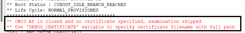
Figure 21 displays the error log in the ModusToolbox™ console for the scenario where the debug port is closed (use case 2) and no valid debug certificate is provided
Figure 21.
Console log for debug port closed
Place the generated file in the ModusToolbox™ debug configuration (Go to ) as shown in Figure 22
Figure 22.
Debug certificate navigation in ModusToolbox™
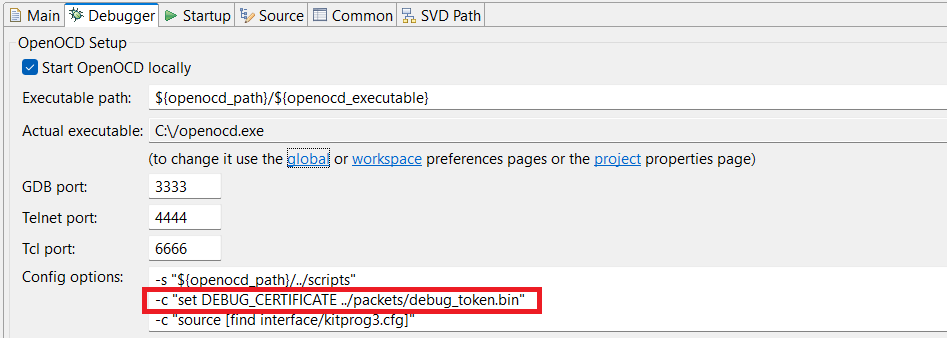
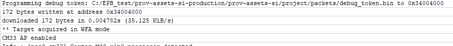
Figure 23 displays the log in the ModusToolbox™ console for the scenario where the debug port is open (use case 2) and a valid debug certificate is provided
Figure 23.
Console log for CM33 AP port enabled
Generating RMA certificate
To create an RMA token
Ensure the "rma" field in the packet/debug_token.json template is Enable
From the project directory, run the following command to generate the token
edgeprotecttools -t psoc_c3 debug-token --template packets/debug_token.json --key keys/oem_rot_priv_key_0. pem -o packets/debug_token.bin
To transition the device to RMA LCS
Ensure that the device is in NORMAL_PROVISIONED or SECURE LCS
For transition into RMA LCS, use the token generated in the previous step. From the project directory, run the following command
edgeprotecttools -t psoc_c3 transit-to-rma --token packets/debug_token.bin
Default debug_token.json file
Code Listing 9
{
"version": "1.0.0.0",
"silicon_id": "0xEE40",
"family_id": "0x0118",
"si_revision_id": "0x11",
"control_word": {
"cm33_ap": "Enable",
"sys_ap": "Enable",
"cm33_dbg": "Enable",
"cm33_nid": "Enable",
"cm33_spid": "Enable",
"cm33_spnid": "Enable",
"cm33_secure": "Enable",
"sys_secure": "Enable",
"rma": "Enable"
},
"die_id": {
"min": {
"lot": 0,
"wafer": 0,
"xpos": 0,
"ypos": 0,
"sort": 0,
"minor": 0,
"day": 0,
"month": 0,
"year": 0
},
"max": {
"lot": 16777215,
"wafer": 255,
"xpos": 255,
"ypos": 255,
"sort": 255,
"minor": 255,
"day": 255,
"month": 255,
"year": 255
}
}
}
Edge Protect Bootloader
The Edge Protect Bootloader (EPB) is a secure bootloader designed to provide a robust and reliable solution for the PSOC™ Control C3 MCU. The key benefits of Edge Protect Bootloader is that Infineon provides it with its source code, giving you the flexibility to choose and customize the bootloader according to your end-product requirements. This bootloader offers a range of advanced features, including seamless software upgrades, image encryption, serial logging, and upgrade by swap capabilities.
Boot flow
OEM will use the Edge Protect Bootloader as an optional bootloader. Its primary functions include: initializing the minimal required hardware, authenticating the next stage application, and launching the application.
Figure 24.
Edge Protect Bootloader with boot one slot configuration
Architecture
Edge Protect Bootloader is based on an open-source MCUboot bootloader library as its foundation and integrates with a range of other components. These include Mbed TLS for secure communication, cryptography hardware driver for cryptographic operations, retarget-io for input/output management, and Peripheral Driver Library (PDL) for peripheral control.
Figure 25.
Edge Protect Bootloader architecture
The Edge Protect Bootloader always boots the application from the primary slot and overwrite/swap the image from the secondary slot into the primary slot when an upgrade is requested.
Edge Protect Bootloader features
The Edge Protect Bootloader offers customizable features that can be tailored to meet specific user requirements through the use of JSON configuration files. These JSON files are located in the
platforms\PSC3\memory_maps
directory and are denoted by the *
.json
extension. By modifying these files, you can configure the Edge Protect Bootloader's features to suit your needs.
After the feature set has been modified, it is necessary to rebuild the application, and reload it onto the device to apply the changes. This ensures that the updated configuration takes effect and the Edge Protect Bootloader operates according to the new settings.
File name | Description |
|---|---|
feature_config.json | Features can be configured by 'set ' or 'false' |
platform.json | Edge Protect Bootloader memory attributes can be configured in this file |
overwrite_single_flash.json | Single image firmware upgrade by overwrite feature can be configured in this file |
overwrite_multi2_flash.json | Multi image firmware upgrade overwrite feature can be configured in this file |
swap_single_flash.json | Single image firmware upgrade by swap feature can be configured in this file |
swap_multi2_flash.json | Multi image firmware upgrade by swap feature can be configured in this file |
Power fail-safe update
If the Edge Protect Bootloader resets in the middle of a swap operation, the two images may be discontiguous in user flash memory. Bootutil recovers from this condition by using the image trailers to determine how the image parts are distributed in flash. The first step is to determine where the relevant swap status region is located. Because this region is embedded within the image slots, its location in the flash changes during a swap operation, see the
reset recovery
. After the swap operation has been complete, the Edge Protect Bootloader proceeds as though it had just been started.
Multi image authentication
The Edge Protect Bootloader offers enabling authentication and upgrade of multiple images before launching the primary application. This process can be configured to either overwrite or swap images, depending on the specified settings. These settings are defined through a JSON file, which provides a flexible and customizable approach to image management.
In the case of the multi-image overwrite method, users are required to configure the
overwrite_multi2_flash.jsonfile
Code listing 10
{
"bootloader":
{
"bootloader_area":
{
    "address"           : "0x32000000",
    "size"              : "0x18000"
},

"ram":
{
    "address"           : "0x34000000",
    "size"              : "0xF000"
},

"shared_data":
{
    "address"           : "0x3400F000",
    "size"              : "0x1000"
}
},

"application_1":
{
"slots":
{
    "boot"              : "0x32018000",
    "upgrade"           : "0x32020000",
    "size"              : "0x8000"
},

"ram":
{
    "address"           : "0x34000000",
    "size"              : "0xF000"
}
},

"application_2":
{
"slots":
{
    "boot"              : "0x32028000",
    "upgrade"           : "0x32030000",
    "size"              : "0x8000"
},

"ram":
{
    "address"           : "0x34000000",
    "size"              : "0xF000"
}
}
}
In the case of the multi-image swap method, configure the
swap_multi2_flash.jsonfile. These files serves as a crucial component in the image upgrade process, allowing you to tailor the overwrite or swap behavior to the specific needs
Code Listing 11
{
"bootloader":
{
"bootloader_area":
{
    "address"           : "0x32000000",
    "size"              : "0x18000"
},

"scratch_area":
{
    "address"           : "0x32038000",
    "size"              : "0x2000"
},

"status_area":
{
    "address"           : "0x3203A000",
    "size"              : "0x2800"
},

"ram":
{
    "address"           : "0x34000000",
    "size"              : "0xF000"
},

"shared_data":
{
    "address"           : "0x3400F000",
    "size"              : "0x1000"
}
},

"application_1":
{
"slots":
{
    "boot"              : "0x32018000",
    "upgrade"           : "0x32020000",
    "size"              : "0x8000"
},

"ram":
{
    "address"           : "0x34000000",
    "size"              : "0xF000"
}
},

"application_2":
{
"slots":
{
    "boot"              : "0x32028000",
    "upgrade"           : "0x32030000",
    "size"              : "0x8000"
},

"ram":
{
    "address"           : "0x34000000",
    "size"              : "0xF000"
}
}
}
To ensure a secure boot process with Edge Protect Bootloader, the device must be provisioned with the BOOT_ONE_SLOT configuration. This setup enables the BootROM to authenticate the first user image, which in this scenario is the Edge Protect Bootloader, and then the Edge Protect Bootloader is responsible for authenticating further additional images that are loaded. This hierarchical approach provides an added layer of security and ensures that only trusted images are executed on the device.
Upgrade by overwrite
The Edge Protect Bootloader always boot from the primary slot and when an upgrade is requested, it copies the new image from the secondary slot into the primary slot. There are two possible upgrade modes: overwrite-based and swap-based.
In overwrite-based mode, the existing image in the primary slot is replaced and if the new image has issues, there is no possibility of rolling back to the previous version. In swap-based mode, the Edge Protect Bootloader preserves the original image, allowing for a potential rollback if needed.
Figure 26.
Upgrade by overwrite
Upgrade by swap
When a swap-based upgrade is enabled, the Edge Protect Bootloader exchanges the images between the primary and secondary slots, allowing for a seamless rollback to the previous version if the upgraded image proves to be faulty. This process involves simultaneously copying the content of the primary slot to the secondary slot and vice versa, effectively preserving both versions of the application on the device.
Once the upgraded firmware is swapped to the primary slot, the Edge Protect Bootloader verifies its operability. If the upgraded image fails to boot, the Edge Protect Bootloader initiates a revert procedure, rolling back to the previous firmware in the primary slot, ensuring a safe and reliable upgrade process.
Figure 27.
Upgrade by swap
Secure boot
Secure boot functionality ensures a trusted boot process through a combination of immutable boot code and digital signatures. The immutable BootROM code serves as the root of trust, launching the Edge Protect Bootloader only after verifying its digital signature. This verified Edge Protect Bootloader, in turn, checks the digital signature of the user application before allowing it to run. If any authentication fails, the device will not boot.
To maintain the integrity of the boot process, the signature verification takes place every time the device boots. This verification occurs in the primary slot. Additionally, the Edge Protect Bootloader verifies the signature of the image in the secondary slot before copying it to the primary slot, ensuring that only authenticated images are used.
Secure boot can be configured through
feature_config.json
file present in the
<CE workspace\platforms\PSC3>
Code Listing 12
"validation_key": {
"description": "Key for image validation",
"value" : "Path to key, TBD"
},
"validate_boot": {
"description": "Image validation during boot",
"value": true
},
"validate_upgrade": {
"description": "Image validation during upgrade",
"value": true
},
During the Edge Protect Bootloader build, it is necessary to provide the private key that will be used to digitally sign the Edge Protect Bootloader. This private key is essential for ensuring the authenticity and integrity of the Edge Protect Bootloader.
make build_proj BOOT_MODE=signed OEM_KEY_FILE=./oem_rot_priv_key_0.pemFor a more in-depth look at the Edge Protect Bootloader implementation for the PSOC™ Control C3 devices, see the Edge Protect Bootloader code example.
Note: When secure boot is enabled, it is essential to configure the boot process accordingly. Specifically, the boot configuration should not be set to BOOT_SIMPLE_APP, as this would compromise the security features of the secure boot process.
Secure firmware update
The Edge Protect Bootloader is important in authenticating firmware during device startup and facilitating firmware switching during the update process. However, it does not have the capability to update the firmware independently. Instead, it relies on external middleware to download new firmware images. Infineon provides two options for this purpose: Device Firmware Update (DFU) middleware for wired updates (via UART, I2C, SPI, or CAN FD) and firmware upgrade via BootROM DFU serial interface (UART, I2C, and SPI).
These middleware solutions can be integrated into end application, enabling communication with the host and downloading of MCUboot-compatible hex files for new firmware images. When using a DFU middleware-based user application, the new image is downloaded to the secondary slot, and control is transferred to the Edge Protect Bootloader. The bootloader then verifies the image version, performs additional validation checks, and depending on the configuration, either swaps or overwrites the image in the secondary slot with the primary boot slot if the secondary slot is valid.
After transferring the image to the primary slot, the Edge Protect Bootloader verifies the primary image and boots to it if verified. Code examples demonstrating firmware upgrade support in end applications for the Edge Protect Bootloader over wired connections on PSOC™ Control C3 devices are available, including:
PSOC™ Control MCU: Firmware upgrade through DFU MW
PSOC™ Control MCU: Factory programming through BootROM DFU
For more information on incorporating DFU middleware into your application or Edge Protect Bootloader, see the
AN236282 - Device Firmware Update (DFU) middleware (MW) for ModusToolbox™
application note.
Image encryption
To ensure the confidentiality of image data during transportation to a device, Edge Protect Bootloader provides a feature to encrypt and decrypt images in real-time during the upgrade process. To utilize this feature, the image header must be flagged as ENCRYPTED (indicated by the value 0x04) and include a Type-Length-Value (TLV) containing the encryption key.
When upgrading an image from the secondary slot to the primary slot, Edge Protect Bootloader automatically decrypts the image after validation. Additionally, if swap upgrades are enabled, Edge Protect Bootloader re-encrypts the image located in the primary slot, which must also have the ENCRYPTED flag set and the TLV present, when swapping it to the secondary slot.
Image encryption can be enabled through
feature_config.json
file present in the
<CE workspace\platforms\PSC3>
.
Code Listing 13
"image_encryption": {
"description": "Activate/deactivate image encryption",
"key" : "Path to key, TBD",
"value": true
},
When encrypting an image, only the payload (FW) is encrypted. The header TLVs are still sent as plain data.
Encrypting the image
Generate a new key pair EC-P256. User can skip this step if they want to use existing keys.
edgeprotecttools create-key --format PEM --key-type ECDSA-P256 --output enc_privkey.pem enc_pubkey.pem
Generate C code for public key.
edgeprotecttools convert-key --fmt C_ARRAY -k enc_privkey.pem -o enc_key.c
Open <user project>/bootloader/enc_key.c file and ecdsa_pub_key to enc_priv_key Generate C code for public key. For example,
Code Listing 14
/* Autogenerated by imgtool.py, do not edit. */
const unsigned char enc_priv_key[] = {
0x30, 0x81, 0x87, 0x02, 0x01, 0x00, 0x30, 0x13,
0x06, 0x07, 0x2a, 0x86, 0x48, 0xce, 0x3d, 0x02,
0x01, 0x06, 0x08, 0x2a, 0x86, 0x48, 0xce, 0x3d,
0x03, 0x01, 0x07, 0x04, 0x6d, 0x30, 0x6b, 0x02,
0x01, 0x01, 0x04, 0x20, 0xd5, 0xea, 0xc4, 0x0e,
0x9d, 0xb7, 0x62, 0x7c, 0xb9, 0x40, 0x4f, 0x44,
0x66, 0x7c, 0xa9, 0x4c, 0xae, 0x16, 0x58, 0xd5,
0x2a, 0x43, 0x4d, 0x8b, 0x28, 0xed, 0x6d, 0xad,
0xe5, 0xa9, 0xea, 0x88, 0xa1, 0x44, 0x03, 0x42,
0x00, 0x04, 0x68, 0x18, 0x8f, 0xbf, 0x94, 0xea,
0x58, 0xe5, 0xe0, 0x55, 0x2e, 0x7c, 0x0b, 0x6f,
0x55, 0x36, 0x9e, 0x89, 0x59, 0x3f, 0xee, 0x6c,
0x28, 0xb2, 0xe2, 0x82, 0x0d, 0x01, 0xeb, 0x18,
0x46, 0x15, 0xc8, 0xed, 0x03, 0x35, 0xcb, 0xc5,
0xc3, 0x74, 0x2a, 0xb1, 0xbc, 0x42, 0x7e, 0x65,
0x36, 0xc9, 0x8d, 0xbc, 0x92, 0x33, 0x14, 0xc4,
0xa1, 0xf7, 0xca, 0x26, 0xe2, 0xcd, 0xf8, 0xfb,
0x15, 0x56
};
const unsigned int enc_priv_key_len = 138;
Build the Edge Protect Bootloader project in the ModusShell with keys to sign the Edge Protect Bootloader
make build_proj BOOT_MODE=signed OEM_KEY_FILE=./oem_rot_priv_key_0. pem
Build and sign the user application with --encrypt command using Edge Protect Tools as follows:
Code Listing 15
ADDITIONAL_ARGS+=--public-key-format full		        \
		--pubkey-encoding raw	        \
		--signature-encoding raw        \
		--overwrite-only                \
                        -- encrypt

POSTBUILD+=$(EPT_PATH) sign-image				\
	--image $(INPUT_IMAGE) 			\
	--output $(OUTPUT_IMAGE) 		\
	--header-size $(HDR_OFFSET)		\
	--slot-size $(SLOT_SIZE)		\
	--key $(KEY_PATH)			\
	--hex-addr $(APP_START_ADDR) 		\
	--align $(FLASH_ALIGNMENT) 		\
	--image-version $(IMAGE_VERSION)	\
	--erased-val $(ERASED_VAL) 		\
	--min-erase-size $(MIN_ERASE_SIZE) 	\
	-s $(RB_COUNTER)			\
	$(ADDITIONAL_ARGS)			\
	--boot-record secureBoot
After programming both Edge Protect Bootloader and user application, Edge Protect Bootloader uses its internal enc_priv_key to decrypt the TLV containing the key. Given that no errors are found, it will then start the validation process, decrypting the blocks before check. A good image being determined, the upgrade consists in reading the blocks from the
secondary slot, decrypting and writing to theprimary slotand Edge Protect Bootloader launches the user application
Downgrade prevention
Downgrade prevention is a security mechanism that ensures a device's firmware can only be updated with a newer version that has a higher security counter number than the existing one. This safeguard prevents malicious attempts to rollback the device to an earlier version, potentially vulnerable firmware version, thereby maintaining the integrity of the device's security.
The software-based downgrade prevention mechanism involves a comparison of image version numbers to prevent the installation of older firmware versions. This feature can be enabled by setting the sw_downgrade_prev parameter present in the <CE workspace\platforms\PSC3feature_config.json> file. However, it is essential to note that this feature is only functional when the overwrite-based image update strategy is employed, which requires the default MEMORY_MAP should be predefined for each platform inside the common.mk file as follows:
MEMORY_MAP ?= ../platforms/$(PLATFORM)/memory_maps/overwrite_single_flash.json
Download prevention can be configured through
feature_config.json
file located in the
<CE workspace\platforms\PSC3>
.
Code Listing 16
"sw_downgrade_prev": {
"description": "Use software downgrade prevention (for 'overwrite' method only!)",
"value": true
}
Dependency check
The Edge Protect Bootloader has the capability to manage multiple firmware images. While it is possible to update these images independently, additional Type-Length-Value (TLV) entries can be added to the protected TLV area following each image.
Dependency check can be configured through feature_config.jsonfile located in the <CE workspace\platforms\PSC3>.
Code Listing 17
 "dependency_check": {
"description": "To prevent upgrading the non-compatible images for multiple-images",
"value": true
},
During the dependency check phase, the Edge Protect Bootloader verifies whether all image dependencies are satisfied. If any image dependency is unfulfilled, modify the swap type of that image accordingly, and restart the dependency check. This process continues until the number of unsatisfied dependencies decreases or remains the same. There is always at least one valid configuration. In the worst-case scenario, the system reverts to its initial state after the dependency check.
A dependency can be specified as an additional parameter while generating the MCUboot format image using the Edge Protect Tool.
For example, -d "(image_id,image_version)", where the image_id is the number of the image
which the current image depends on and the image_version is the minimum version of that image to satisfy compliance. For example, -d "(1, 1.2.3+0)" means that this image depends on Image 1, which version has to be at least 1.2.3+0.
Fault injection hardening
To counteract hardware-based fault injection attacks, such as power glitching and EM pulses, which aim to execute unauthorized code, the Edge Protect Bootloader incorporates software-based countermeasures. These attacks use induced changes in CPU behavior, including skipped instructions, modified registers, corrupted memory reads, and altered instruction decoding to bypass security mechanisms.
While these software countermeasures enhance the resistance to fault injection
attacks, they do not provide complete protection. The level of protection can be
controlled using the MCUBOOT_FIH_PROFILE_* macros, which offer four
levels of protection: none, moderate, medium, and maximum. These countermeasures are
primarily integrated into the core MCUboot codebase, focusing on critical code paths
that are susceptible to fault injection. Additionally, independent cryptographic
libraries, such as mbed-crypto or tinycrypt can offer further protections, but this
requires separate assessment.
The key hardening code is located in the following files:
boot/bootutil/include/bootutil/fault_injection_hardening.h
boot/bootutil/src/fault_injection_hardening.c
The fault injection mitigation library provides support for various measures, which can be enabled or disabled individually or by defining one of the MCUBOOT_FIH_PROFILEs. For more information on the measures supported by each profile, see the
fault_injection_hardening.h
file and
boot\cypress\MCUBootApp\MCUBoot.mk
file.
Serial logging
During the boot and upgrade process, the Edge Protect Bootloader is designed to log its status and reports, transmitting this information over a serial port. The level of detail in these logs is determined by the compiled log level, which sets the maximum amount of information that can be recorded. By default, these logs are printed over a UART port. Notably, this feature can be enabled or disabled during the compilation process, allowing for customization of the logging behavior.
There are five log-levels with a unique value defined in the Edge Protect Bootloader in the
\boot\cypress\MCUBootApp\config\mcuboot_config\mcuboot_logging.h
file.
#define MCUBOOT_LOG_LEVEL_OFF      0
#define MCUBOOT_LOG_LEVEL_ERROR    1
#define MCUBOOT_LOG_LEVEL_WARNING  2
#define MCUBOOT_LOG_LEVEL_INFO     3
#define MCUBOOT_LOG_LEVEL_DEBUG    4
You can define the global logging level by defining any of the above-mentioned log-levels in the
application>/bootloader_app/Makefile
.
MCUBOOT_LOG_LEVEL sets the minimum level that will be logged. The function priority is:
MCUBOOT_LOG_ERR > MCUBOOT_LOG_WRN > MCUBOOT_LOG_INF > MCUBOOT_LOG_DBG
Policy file
The policy file controls aspects of the boot procedure that requires to be assigned during provisioning before running the first OEM code.
Table 12
describes the common parameters that can be set by the OEM.
Parameter | Application values | Default value | Description |
|---|---|---|---|
Device policy | |||
target_lcs | NORMAL_PROVISIONED, SECURE | NORMAL_PROVISIONED | The device will be shipped to an OEM in this LCS. |
nc_counter_l1 | 0 | 0 | L1 application NV counter. 0, if no update. |
nv_counter_l2 | 0 | 0 | L2 application NV counter. 0, if no update. |
prov_oem_complete | false, true | FALSE | Indicates that all OEM assets are finalized in SFlash and no further update is allowed. After this, the flag is set and provisioned. OEM can do only re-provisioning and RMA if needed. |
debug | |||
ap_cm33 | Enable, Disable, Permanently Disable | Enable | Configures the CM33 debug access port availability in the SECURE and NORMAL_PROVISIONED LCS. |
listen_window | 100 ms, 20 ms, 1 ms, 0 ms | 100 ms | Configures the listen window time to acquire the CM33 debug access port in the SECURE LCS. |
cm33_dbg | Enable, Disable, Permanently Disable | Enable | Invasive Debug. It implies that non-invasive is also enabled. |
cm33_nid | Enable, Disable, Permanently Disable | Enable | Non-Invasive Debug (monitoring without control). |
cm33_spid | Enable, Disable, Permanently Disable | Enable | Secure Privileged Invasive Debug. The control field is not applicable in the development LCS. |
cm33_spnid | Enable, Disable, Permanently Disable | Enable | Secure Privileged Non-Invasive Debug. The control field is not applicable in the development LCS. |
cm33_Secure | Enable, Disable, Permanently Disable | Enable | Secure Privileged Debug. The control field is not applicable in the development LCS. |
system | |||
ap | Enable, Disable, Permanently Disable | Enable | System access port (SYS-AP) restriction. |
secure | Enable, Disable, Permanently Disable | Enable | Enables the CM33 secure application interface. |
boot | |||
boot_cfg_id | BOOT_SIMPLE_APP, BOOT_ONE_SLOT, BOOT_TWO_SLOTS, BOOT_THREE_SLOTS, BOOT_IDLE | BOOT_SIMPLE_APP | Boot configuration. |
boot_dual_bank_enable | false, true | false | Flag to enable flash dual bank feature. |
boot_bank_ctr_addr | 0xC39D5455 | – | An address of a 32-bit counter for flash dual bank switching. |
boot_auth_l1 | Fast, Full | Full | Fast or full authentication configuration for first application. |
boot_auth_l2 | Fast, Full | Full | Fast or full authentication configuration for the second application. |
boot_auth_l2_enable | false, true | true | Indicates whether to enable second application authentication by Boot firmware. |
boot_move_layout | false, true | – | Indicates whether the L2 application overwrites the L1 application. Relevant for the case when there is an application in the second slot. |
boot_app_layout | – | – | The memory layout for the applications defined by the BOOT_CFG_ID. |
dfu | |||
dfu_enable | false, true | false | Flag to enable the BootROM DFU serial interface. |
dfu_l1_update | false, true | false | Indicates whether to allow L1 update with BootROM DFU. |
boot_od_clk | 48 MHz, 100 MHz, 180 MHz | 180 MHz | CM33 boot frequency options. |
mpc | |||
mpc_struct_ram | – | – | RAM MPC structures. The total number of RAM and flash MPC structures. |
mpc_struct_flash | – | – | Flash MPC structures. The total number of RAM and flash MPC structures. |
pre_build | – | – | – |
keys | |||
oem_rot_public_key_0 | – | – | Key path for the first application OEM rot key 0. |
oem_rot_public_key_1 | – | – | Key path for the first application OEM rot key 1. |
Appendix A. Default OEM provisioning policy
The default OEM policy parameters are preset on a device before it is shipped to the OEM.
Code Listing 18
{
"policy": {
"platform": "psoc_c3",
"version": 1.0,
"type": "oem_provisioning"
},
"device_policy": {
"target_lcs": {
"description": "The LCS to which the transition should be done",
"applicable_conf": "NORMAL_PROVISIONED, SECURE",
"value": "NORMAL_PROVISIONED"
},
"program_sflash_assets": {
"description": "Indicates whether to program the assets which are placed into SFLASH",
"value": true
},
"program_iak": {
"description": "Indicates whether to generate and program Initial Attestation Key",
"value": true
},
"program_hash": {
"description": "Enables ASSET_HASH and FACTORY_HASH validation in NORMAL_PROVISIONED LCS",
"value": false
},
"nv_counter_l1": {
"description": "L1 application NV counter. 0, if no update",
"value": 0
},
"nv_counter_l2": {
"description": "L2 application NV counter. 0, if no update",
"value": 0
},
"prov_oem_complete": {
"description": "Indicates OEM assets are finalized in SFLASH",
"warning": "Once the 'prov_oem_complete' parameter value is set to true, it cannot be changed! No further updates to SFLASH are allowed",
"value": false
},
"debug": {
"cpu": {
  "ap_cm33": {
    "description": "Configures the CM33 debug access port availability in the SECURE and NORMAL_PROVISIONED LCS",
    "applicable_conf": "Enable, Disable, Permanently Disable",
    "value": "Enable"
  },
  "listen_window": {
    "description": "Configures the listen window time to acquire the CM33 debug access port in the SECURE LCS",
    "applicable_conf": "100 ms, 20 ms, 1 ms, 0 ms",
    "value": "100 ms"
  },
  "cm33_dbg": {
    "description": "Configures the invasive debug of CM33 core",
    "applicable_conf": "Enable, Disable, Permanently Disable",
    "value": "Enable"
  },
  "cm33_nid": {
    "description": "Configures the non-invasive debug of CM33 core",
    "applicable_conf": "Enable, Disable, Permanently Disable",
    "value": "Enable"
  },
  "cm33_spid": {
    "description": "Configures the secure privileged invasive debug of CM33 core",
    "applicable_conf": "Enable, Disable, Permanently Disable",
    "value": "Enable"
  },
  "cm33_spnid": {
    "description": "Configures the secure privileged non-invasive debug of CM33 core",
    "applicable_conf": "Enable, Disable, Permanently Disable",
    "value": "Enable"
  },
  "cm33_secure": {
    "description": "Enables the CM33 secure AP interface",
    "applicable_conf": "Enable, Disable, Permanently Disable",
    "value": "Enable"
  }
},
"system": {
  "ap": {
    "description": "Configures the System debug access port availability in the SECURE and NORMAL_PROVISIONED LCS",
    "applicable_conf": "Enable, Disable, Permanently Disable",
    "value": "Enable"
  },
  "secure": {
    "description": "Enables the system secure AP interface",
    "applicable_conf": "Enable, Disable, Permanently Disable",
    "value": "Enable"
  },
  "mmio_restrictions": {
    "description": "MMIO restrictions for System AP",
    "applicable_conf": "No restrictions, SRSS_GENERAL2 only, No access",
    "value": "No restrictions"
  },
  "debug_pins": {
    "description": "Configures debug pins and interface",
    "comment_1": "0000 - 2 pins (TMS, TCLK), JTAG is disabled",
    "comment_2": "0011 - 2 pins (TMS, TCLK), JTAG is enabled",
    "comment_3": "0101 - 4 pins (TMS, TCLK, TDO, TDI)",
    "comment_4": "0110 - 5 pins (TMS, TCLK, TDO, TDI, TRSTN)",
    "comment_5": "1001 - SWJ pins disabled, JTAG is enabled",
    "comment_6": "1010 - SWJ pins disabled, JTAG is disabled",
    "applicable_conf": "0000, 0011, 0101, 0110, 1001, 1010",
    "value": "0000"
  }
}
},
"boot": {
"boot_cfg_id": {
  "description": "A behavior for BOOT_APP_LAYOUT (BOOT_SIMPLE_APP applicable to NORMAL_PROVISIONED only)",
  "applicable_conf": "BOOT_SIMPLE_APP, BOOT_ONE_SLOT, BOOT_TWO_SLOTS, BOOT_THREE_SLOTS, BOOT_IDLE",
  "value": "BOOT_SIMPLE_APP"
},
"boot_dual_bank_enable": {
  "description": "Indicates whether to enable flash dual bank feature",
  "value": false
},
"boot_bank_ctr_offset": {
  "description": "An offset from the start of each flash bank where a 32-bit counter for flash dual bank switching is placed",
  "value": "0xC39D5455"
},
"boot_auth_l1": {
  "description": "Fast or full authentication configuration for L1 application",
  "applicable_conf": "Fast, Full",
  "value": "Full"
},
"boot_auth_l2": {
  "description": "Fast or full authentication configuration for L2 application",
  "applicable_conf": "Fast, Full",
  "value": "Full"
},
"boot_auth_l2_enable": {
  "description": "Indicates whether to enable L2 slot authentication by Boot FW",
  "value": false
},
"boot_move_app": {
  "description": "Indicates whether the L2 application overwrites the L1 application. Relevant for the case when there is an application in the second slot",
  "value": false
},
"boot_app_layout": {
  "description": "The memory layout for the applications defined by BOOT_CFG_ID. 0x32000000 - 0x33FFFFFF for secure addresses; 0x22000000 - 0x23FFFFFF for non-secure addresses",
  "value": [
    {
      "address": "0x32000000",
      "size": "0x40000"
    },
    {
      "address": "0x00000000",
      "size": "0x00"
    },
    {
      "address": "0x00000000",
      "size": "0x00"
    }
  ]
}
},
"dfu": {
"dfu_enable": {
  "description": "Indicates whether Device Firmware Update is enabled",
  "value": true
},
"dfu_l1_update": {
  "description": "Indicates whether to allow L1 update with DFU",
  "value": true
}
},
"boot_od_clk": {
"description": "CM33 boot frequency",
"applicable_conf": "48 MHz, 100 MHz, 180 MHz",
"value": "180 MHz"
},
"pc1_ctl_valid": {
"description": "True when 'pc1_handler' is valid",
"value": false
},
"pc2_ctl_valid": {
"description": "True when 'pc2_handler' is valid",
"value": false
},
"pc3_ctl_valid": {
"description": "True when 'pc3_handler' is valid",
"value": false
},
"pc1_handler": {
"description": "Used to switch to PC1 when it is a 'Special' PC",
"value": "0xFFFFFFFF"
},
"pc2_handler": {
"description": "Used to switch to PC2 when it is a 'Special' PC",
"value": "0xFFFFFFFF"
},
"pc3_handler": {
"description": "Used to switch to PC3 when it is a 'Special' PC",
"value": "0xFFFFFFFF"
},
"mpc": {
"mpc_struct_ram": {
  "description": "RAM MPC structures. The total number of RAM and Flash MPC structures must be less than 32",
  "value": [
    {
      "description": "Offset and size in KB. The values must be multiple of 2 (e.g. 0 KB, 2 KB, 4 KB, 8 KB, ...)",
      "offset": "0 KB",
      "size": "2 KB",
      "attr": {
        "description": "The MPC attributes for this memory region",
        "comment_1": "WRN allow write, read, and NS only access",
        "comment_2": "-RN allow read, NS-only access",
        "comment_3": "--- and --N, no access",
        "comment_4": "WR- read and write access, but NS=0 only",
        "value": {
          "pc0": "WR-",
          "pc1": "WR-",
          "pc2": "WR-",
          "pc3": "WR-",
          "pc4": "WR-",
          "pc5": "WR-",
          "pc6": "WR-",
          "pc7": "WR-"
        }
      }
    }
  ]
},
"mpc_struct_flash": {
  "description": "Flash MPC structures. The total number of RAM and Flash MPC structures must be less than 32",
  "value": [
    {
      "description": "Offset and size in KB. The values must be multiple of 2 (e.g. 0 KB, 2 KB, 4 KB, 8 KB, ...)",
      "offset": "2 KB",
      "size": "2 KB",
      "attr": {
        "description": "The MPC attributes for this memory region",
        "comment_1": "WRN allow read, write, and NS only access",
        "comment_2": "-RN allow read, NS-only access",
        "comment_3": "--- and --N, no access",
        "comment_4": "WR- read and write access, but NS=0 only",
        "comment_5": "W--, W-N illegal values",
        "value": {
          "pc0": "WR-",
          "pc1": "WR-",
          "pc2": "WR-",
          "pc3": "WR-",
          "pc4": "WR-",
          "pc5": "WR-",
          "pc6": "WR-",
          "pc7": "WR-"
        }
      }
    }
  ]
}
}
},
"pre_build": {
"keys": {
"oem_rot_public_key_0": {
  "description": "Path to the OEM RoT public key 0",
  "value": "../keys/oem_rot_pub_key_0.pem"
},
"oem_rot_public_key_1": {
  "description": "Path to the OEM RoT public key 1",
  "value": "../keys/oem_rot_pub_key_1.pem"
}
}
},
"raw_data_pc012": {
"description": "Path to a binary file containing custom data accessible in PC0, PC1, and PC2. Up to 256 bytes",
"value": ""
}
}
References
For a complete and up-to-date list of PSOC™ Control C3 MCU code examples, see Infineon
GitHub
page. For additional PSOC™ Control C3 MCU-related documents, see the
PSOC™ Control C3 MCU
,
PSOC™ Control C3P
, and
PSOC™ Control C3M
webpages.
Application notes
AN238329 - Getting started with PSOC™ Control C3 MCU on ModusToolbox™ software
AN236282 - Device Firmware Update (DFU) middleware (MW) for ModusToolbox™
Datasheets
002-36422: PSOC™ Control C3 - PSC3P2xD, PSC3M3xD
002-36032: PSOC™ Control C3 - PSC3P5xD, PSC3M5xD
Guide
002-39527: PSOC™ Control C3 MCU hardware design guide
Reference manuals
Glossary
If you are new to embedded device security and/or new to Infineon's line of PSOC™ Control C3 devices, some of the terminology can be new to you. The following is a list of terms that will be used throughout the document:
Concise binary object representation (CBOR): This format is used to store the owner's policy in the device's NVM
Debug access port (DAP): There may be multiple DAPs in this device accessible to the customer; system, CM33
Development LCS: This is the stage that the device is in during development. In this stage, no permanent changes are made to the device, and it can be reverted back to its original state that was shipped from Infineon. The device can be provisioned as many times as needed while in this stage
Device firmware upgrade (DFU): DFU is the act of transferring data from the host to the target flash either using a BootROM DFU or customer DFU interface and booting to newly downloaded firmware
Hash: A crypto algorithm that generates a repeatable but unique signature for a given block of data. This function is not reversible
IPC: Inter-processor communication. Hardware used to facilitate communication between secure and non-secure environment
Lifecycle stage (LCS): The device is shipped from Infineon in the development LCS and then will be advanced to the production LCS when the customer ships the product
MCUboot: An open-source secure bootloader library for 32-bit MCUs aiming to define a common infrastructure for the bootloader and system flash layout on microcontroller systems and to provide a secure bootloader that enables easy software upgrade
Memory protection unit (MPU): Hardware blocks used to allow or deny access to sections of memory or peripherals to bus masters
Non-volatile memory (NVM): A type of memory that can retain stored information even after power is removed
OEM: Original Equipment Manufacturer
Infineon's customers OEM_Policy: This file contains the boot-up parameters used
OEM_ROT_KEY: This refers to the OEM_ROT_PUBLIC_KEY and OEM_ROT_PRIVATE_KEY pairs
OEM_ROT_PRIVATE_KEY: This key is used to sign the first OEM code in the system when secured boot is enabled. This key can also be used to sign other projects or firmware updates that are installed on the device
OEM_ROT_PUBLIC_KEY: This is the key used to validate the first OEM code when secured boot is enabled
Production LCS: Once a device is transitioned to this stage, it cannot revert back to the development LCS
Provision: This is the process by which the OEM loads their custom software, keys, and boot parameters into the device. A textual, JSON-formatted file (OEM_POLICY) is used to define a set of security-related parameters
Primary code space: This is the location in memory where the code to be executed is stored in non-volatile memory
RAM APP: Executable code that is loaded into SRAM. RAM APP can be written and loaded by the OEM and is executed by the CM33
Return merchandise authorization (RMA): This LCS is used if a device is suspected to be defective. The OEM places the device in this stage prior to shipment back to Infineon
Root of trust (RoT): In the PSOC™ Control C3 devices, the BootROM code is the root of trust
Secondary code space: This is the area where code updates are stored until they have been copied into the primary
Secured boot: In the context of this document, this refers to when the first OEM code must be signed and then authenticated by the boot code
Serial Wire Debug (SWD): A method used to interface debug and programming tools to the device
TLV: Tag-length-value is a way of storing data in a project header that is easily parsed by code
Revision history
Document revision | Date | Description of changes |
|---|---|---|
** | 2024-09-19 | Initial release |
*A | 2024-12-12 | Updated Secure boot section Added the following sections: |