AN228680 Secure system configuration in TRAVEO™ T2G family
About this document
Scope and purpose
This document explains the requirements to configure a secure system from the boot process to application software execution in the TRAVEO™ T2G family.
Intended audience
This document is intended for anyone who uses the TRAVEO™ T2G family to configure a secure system.
Associated part family
TRAVEO™ T2G family
Introduction
This application note discusses how to make sure that the system executes code only from a trusted source and how to configure a secure embedded system using TRAVEO™ T2G family MCUs. You will learn about the boot process and how it pertains to a secure system.
This is an advanced application note and assumes that you are familiar with the basic TRAVEO™ T2G architecture (see the device datasheet [1] or the architecture technical reference manual (TRM) [2]).
There are many reasons why a system must be secure: manufacturers want to protect their IP to maintain their market, or to protect the end user from dangerous operations caused by a malicious attack from a third party.
There are three main ways products can be hacked:
- Direct access to the debug port : TRAVEO™ T2G is based on Arm® architecture; accessing or reprogramming firmware or examining internal data is easy with the use of a common debugger. Hacking or reverse engineering a product is easy if the device is left unsecured.
- Direct connection to a communication port such as SPI, I2C, CAN, LIN, or a UART : These ports are used for communication between ECUs, or between the ECU and other components in the car. It is also used for ECU software update or information acquisition. This connection may allow firmware to be read or updated with non-sanctioned access if the device is left unsecured.
- Wireless connection such as OTA : This has become the standard method of hacking because it doesn’t require physical contact. Perpetrators can access the car to perform unauthorized firmware update and control from anywhere if the device is left unsecured.
What is a secure system?
The definition of a secure system can be different depending on the application. Some systems require that all access to the device is blocked, but others just need to verify that the firmware has not been corrupted. The TRAVEO™ T2G MCU allows you to define the security level required for the project. There is no one perfect method because every project has different requirements. The following is a list of projects with different security goals:
- Trusted firmware updates only with a hardware debugger : This is usually not thought of as a secure system, but if the hardware is installed such that third parties cannot get direct access, then it may be secure. Flash write commands from firmware can be disabled so that any internal hack could not change or replace the application. The device can be put in a secure mode with the debug port open, which will force the firmware to be authenticated with a public key each time the device comes out of reset.
- No access to debug port, support firmware updates : The debug port provides access to all memory and a method for the device to be reprogrammed. In most cases, a real secure system requires that the debug port is disabled. Then, the only way to update the firmware is for the application to provide a way to download new program data with some type of communication port such as UART, I2C, CAN, LIN, or SPI. The designer decides how secure this communication port must be.
- Lock down firmware, no updates : This means that the debug port is disabled and there is no provision for bootloading. This may be the most secure, but there is no way to perform bug fixes or add future enhancements.
- Trusted firmware updates, protect IP : To fully protect the IP, the debug port must be disabled. Because the debug port is disabled, the user must provide a method to load new firmware with a bootloader. This is typically implemented with a serial port such as UART, SPI, or I2C. Because the IP must be protected, the bootloader must encrypt the data transferred. The TRAVEO™ T2G MCU includes a crypto block to help accelerate encryption and decryption. Security keys installed in the device at the factory can be used to authenticate the code and decrypt the data transferred during the bootloading process.
Note: All security-related features offered by the TRAVEO™ T2G family MCUs are intended to provide protection only against logical attacks. These are attacks which use regular interfaces to communicate in an unexpected way with the device and can be performed even remotely. Typical examples are buffer overflow, authentication bypass, malicious software injection, misuse of debug functions or interfaces, etc.
Note: Physical attacks are considered out of scope and hence, the TRAVEO™ T2G family MCUs do not contain any hardware countermeasures against non-invasive, semi-invasive, or invasive attacks. Countermeasures against side-channel attacks and fault injection attacks must be implemented by software.
Basic definitions
This section describes some terms that will be used throughout this document.
- Application flash (User) : This is the flash memory that is used to store your application code.
- Chain of Trust (CoT) : The root of trust begins with the code residing in the ROM, which cannot be altered. Chain of Trust is established by validating the blocks of software before the execution starting from the root of trust located in the ROM.
- Cipher-based Message Authentication Code (CMAC) : Message authentication code algorithm based on block cipher. (e.g., AES)
- CySAF : Cypress secure application format
- Debug access port (DAP) : Interface between an external debugger/programmer and TRAVEO™ T2G MCU for programming and debugging. This allows the connection to one of the three access ports (AP), CM0_AP, CM4_AP or CM7_AP, and System_AP. The System_AP can only access SRAM, flash, and MMIOs, not the CPUs.
- DAP access restriction : This determines the debug port access restrictions, and has three states corresponding to the protection state: Normal, Secure, and Dead. Each of these states may be configured by the user. See Security enhance PPU configuration for the storage location of access restriction in each protection state.
- Digital digest/signature : The signature generated by the SHA-256 function that operates on a block of data.
- Electronic Control Unit (ECU) : Unit for controlling the system using electronic circuits; mainly mounted on automobiles. There are various ECUs depending on the application, such as body control, engine control, and brake control.
- eFuse : One Time Programmable (OTP) memory, that by default is ‘0’ and can be changed only from ‘0’ to ‘1’. The eFuse bits can be programmed individually, but cannot be erased.
- eFuse Read Protection Unit (ERPU) : This is part of SWPU (Software Protection Unit, see definition below). ERPUs are used to implement read access restrictions to eFuse.
- eFuse Write Protection Unit (EWPU) : This is part of SWPU. EWPUs are used to implement write access restrictions to eFuse.
- Flash Boot : This is part of the boot system that performs two basic tasks:
- Sets up the debug port based on the lifecycle stage.
- Validates the user application before executing it.
- Flash Write Protection Unit (FWPU) : This is part of SWPU. FWPUs are used to implement write access restrictions to flash.
- Hash : A crypto algorithm that generates a repeatable but unique digest for a given block of data. This function is non-reversible.
- IP : Intellectual Property. This can be both code and data stored in a device.
- IPC : Inter-Processor Communication hardware used to facilitate communication between the two CPU cores.
- Lifecycle : This is the security mode in which the device is operating. TRAVEO™ T2G MCU has five stages NORMAL_PROVISIONED, SECURE, SECURE_W_DEBUG, RMA, and CORRUPTED. To the user, it has only three states of interest: NORMAL_PROVISIONED, SECURE, and SECURE_W_DEBUG.
- Main User Application : This is part of the user application that is not authenticated by flash boot. It is mainly executed by the CM4 or CM7 CPU. For CoT, it needs to be authenticated with the Secure Image.
- Memory Protection Unit (MPU) : MPU is used to isolate memory sections from different software components executed on the same CPU. MPU is bus-master-specific.
- MMIO : Memory-Mapped Input/Output, usually refers to registers that control the hardware I/O.
- Non-Secure (NS) : NS is a protection attribute used to distinguish between secure and non-secure accesses. In non-secure setting, secure access is also allowed. The NS attribute is allowed and restricted by SMPU, PPU, and SWPU.
- Over the Air (OTA) : OTA refers to transmission and reception of data via wireless communication.
- Protection Context (PC) : PC can apply different protection attributes to bus master access without changing the setting of protection units. The PC attribute is allowed and restricted by SMPU, PPU, and SWPU. Although PC most often refers to a Program Counter, in this document, it refers to the Protection Context.
- Peripheral Protection Unit (PPU) : PPUs are used to restrict access to a peripheral or set of peripherals to only one or a specific set of bus masters.
- Protection state : There are Normal, Secure, Dead, and Virgin states depending on the lifecycle stage. ROM boot deploys access restrictions according to the protection status.
- Protection Units : These are four types of protection units: Memory Protection Unit (MPU), Shared Memory Protection Unit (SMPU), Peripheral Protection Unit (PPU), and Software Protection Units (SWPU). MPU, SMPU, and PPU are implemented by hardware; SWPU is implemented by software.
- Public-Key Cryptography (PKC) : Otherwise known as asymmetrical cryptography. Public-key cryptography is an encryption technique that uses a paired public and private key (or asymmetric key) algorithm for secure data communication. It is used to decode a message or block of data. The private key is used to decrypt the data and must be kept secured, while the public key is used to encrypt the data but can be disseminated widely.
- Public Key : The public key can be shared, but it should be authenticated or secured so it cannot be modified.
- Private Key : The private key must be kept in a secure location so it cannot be viewed or stolen. It is used to decrypt a block of data that has been encrypted using an associated public key.
- RMA : Returned Material Authorization
- ROM : Read Only Memory that is programmed as part of the fabrication process and cannot be reprogrammed.
- RSA-nnnn : An asymmetric encryption system that uses two keys. One key is private and should not be shared and the other is public and can be read without loss of security. The encryption/decryption is controlled by a key that is commonly 2048, 3072, or 4096 bits in length (RSA-2048, RSA-3072, or RSA-4096).
- Secure Image : A software that is used to set up the security features such as HSM firmware of TRAVEO™ T2G MCU; it is mainly executed by CM0+. It can be modified by the programmer to implement a specific security policy.
- Security Policy : This is the set of rules that the designer imposes to determine what resources are protected from outside tampering or between the internal CPUs.
- Serial Memory Interface (SMIF) : An SPI (Serial Peripheral Interface) communication interface to serial memory devices, including NOR flash, SRAM, and non-volatile SRAM.
- SFlash : Supervisor flash memory. This memory partition in flash contains several areas that include system trim values, flash boot executable code, public key storage, etc. After the device transitions into a SECURE lifecycle stage, it can no longer be changed.
- SHA-256 : A cryptographic hash algorithm used to create a digest for a block of data or code. This hash algorithm produces a 256-bit unique digest of the data no matter the size of the data block.
- Shared Memory Protection Unit (SMPU) : SMPUs are used to allow access to a specific memory space (flash, SRAM, or registers) to only one or a specific set of bus masters.
- Software Protection Units (SWPU) : SWPUs are used to implement access restrictions to flash write, and eFuse read and write.
- System Calls : Functions such as flash write functions that are executed by the Arm® Cortex® M0+ CPU (CM0+) from ROM.
- TOC1 : This is an area in SFlash that is used to store pointers to the trim values, flash boot entry points, etc. It is used only by boot code in ROM and is not editable by the designer.
- TOC2 : This is an area in SFlash that is used to store pointers to two applications blocks: Secure Image and Main User Application. It also contains some boot parameters that are settable by the system designer.
Lifecycle stage
The device lifecycle is a key aspect of the TRAVEO™ T2G MCU security. Lifecycle stages follow a strict irreversible progression dictated by blowing eFuses (changing a fuse’s value from ‘0’ to ‘1’). This system is used to protect the internal device data and code at the level required by the customer. Figure 1 shows the TRAVEO™ T2G MCU-supported lifecycle stages.
Figure 1. Device lifecycle stages

NORMAL_PROVISIONED
This is the lifecycle stage of a device after trimming and testing is complete in the factory. All configuration and trimming information is complete. Valid flash boot code has been programmed in the SFlash. To allow the OEM to check the data integrity of trims, flash boot, and other objects from the factory, a hash (SHA-256 truncated to 128 bits) of these objects is stored in eFuse. This hash is referred to as FACTORY_HASH. Customers receive parts in this stage.
SECURE
This stage is the lifecycle stage of a secure device. Prior to transitioning to this stage, the SECURE_HASH must have been blown in eFuse and valid application code must have been programmed in the code flash. In this stage, the protection state is set to SECURE and SECURE access restrictions are deployed. A SECURE device will boot only when authentication of its flash boot and application code succeeds. The SECURE_HASH is calculated and written to the eFuse by SROM firmware, when transitioning to the SECURE or SECURE_W_DEBUG lifecycle stage from the NORMAL_PROVISIONED lifecycle stage. See Appendix H -Example programs and scripts for the transition to SECURE lifecycle stage.
Note: Lifecycle stage is irreversible. Therefore, it is recommended that the programming process is evaluation and the application program is authenticated before transitioning to SECURE lifecycle stage.
SECURE_W_DEBUG
This stage is the same as SECURE lifecycle stage, except the device allows for debugging. Prior to transitioning to this stage, the SECURE_HASH must have been blown in eFuse and valid application code must have been programmed in the code flash. In this stage, the protection state is set to SECURE, but NORMAL access restrictions are deployed to enable debugging. When there is an authentication failure during ROM boot or flash boot, the protection state is set to “SECURE” but NORMAL access restrictions are deployed, SWD/JTAG pins are enabled, and is not transitioned to “DEAD” state. Transition from SECURE_W_DEBUG to SECURE is not allowed. SECURE_W_DEBUG parts are used only by the developers and SW testers. Devices should not be shipped in this lifecycle stage. See Appendix H - Example programs and scripts for the transition to SECURE_W_DEBUG lifecycle stage.
RMA
This stage allows one to perform Failure Analysis (FA). The customer transitions the part to RMA lifecycle stage when the customer wants to perform failure analysis on the part. The customer erases all the sensitive data prior to invoking the system call (TransitiontoRMA API) that transitions the part to RMA.
When invoking the system call to transition to RMA, the customer must create a certificate that authorizes to transition the part with a specific Unique ID to RMA lifecycle stage. The certificate will be signed by the customer using the same private key that is used in signing the user application image. The verification of the signature uses the same algorithm used by flash boot in authenticating the user application. The same public key (injected by the OEM) stored in SFlash is used for the verification.
When a part is reset in the RMA lifecycle stage, the boot will set the access restrictions such that the DAP has access only to System AP, IPC MMIO registers for making system calls, and adequate RAM for communication. It will then wait for the system call (OpenRMA API) from the DAP along with the certificate of authorization. The boot process will not initiate any firmware until it successfully executes the OpenRMA API. After the command is successful, the lifecycle stage stored in eFuse cannot be changed from RMA. Every time the part is reset, it must execute the OpenRMA API successfully before the part can be used. To execute the OpenRMA API, the customer must create the certificate signed using their private key. See Appendix E- Transition to RMA lifecycle stage for the transition to RMA lifecycle stage.
Note: The device with a DEAD protection state or CORRUPTED lifecycle stage cannot transition to the RMA lifecycle stage.
Note: It is possible to transition to RMA only from the SECURE or SECURE_W_DEBUG lifecycle stage. Therefore, the device needs to transition to SECURE or SECURE_W_DEBUG and then to RMA, if it is NORMAL_PROVISIONED life cycle stage.
Note: An RSA key pair (private key and public key) is required to run the TransitiontoRMA API. The private key is used to create the certificate and the public key is used to authenticate the certificate. The public key must be written to the device in advance.
Note: An RSA key pair (private key and public key) can be required to run the OpenRMA APIs. The private key is used to create the certificate and the public key is used to authenticate the certificate. The public key must be written to the device in advance. However, if the device was transitioned to the RMA lifecycle stage from the SECURE_WITH_DEBUG lifecycle stage, then OpenRMA is skipped and the device does not wait for OpenRMA execution. Hence full access to the device will be unlocked without the certificate and the user application will be executed.
Note: ECC errors might occur during the execution of the TransitiontoRMA and OpenRMA APIs. Therefore, the user software should be careful in handling failures during the TransitiontoRMA API execution and after the OpenRMA API execution. See Requirements for transition to RMA lifecycle stage for more details.
If the device transitions to a DEAD protection state due to an unintended authentication failure, such as hardware failure or sensitive data erase, and cannot transition to RMA lifecycle stage, you may be able to solve it by preparing a second application software to only allow transition to the RMA lifecycle stage. The start address is defined in TOC2. If the first application software fails or erases all of the first application, Flash Boot can run the second application. However, if the authentication of the second application software is also corrupted, the device cannot transition to the lifecycle stage. The second application software could be exclusively used for RMA management. It is recommended that the second application software is located in a different sector than the first application software, so that only the first application can be erased. See TOC2 for TOC2 details, and Appendix I - Second application software implementation for the second application software implementation.
However, if the device meets the bootloader enabling conditions, the second application cannot be activated when all of the first application has been erased. See the TOC2 for bootloader enabling conditions.
If all of the first application is erased, it can transition to DEAD state. There are two options:
- Case of the second application is not implemented
- Prepare and reprogram the signed dummy code and digital signature, instead of the first application software, after erasing. This dummy code can be exclusively used for RMA management.
- Case of the second application is implemented
- Prepare and reprogram the dummy application header, instead of the first application software, after erasing. See Appendix J - Dummy application header implementation for the application header implementation.
- Disabling the bootloader. (TOC2_FLAGS.FB_BOOTLOADER_CTL=0x2) It is only available in NORMAL_PROVISIONED lifecycle stage.
Requirements for transition to RMA lifecycle stage
This section describes the conditions for the TransitiontoRMA and OpenRMA APIs execution used to transition to the RMA lifecycle stage.
TransitiontoRMA API
ECC errors might occur during the TransitiontoRMA API execution. Therefore, user software should not configure the fault structure for Crypto and SRAM0 ECC errors before triggering the TransitiontoRMA API. Otherwise, the software will ignore the ECC faults reported during the TransitiontoRMA API execution. The following failures need to be masked:
- (Fault number is CYT2B series):
- CPUSS_RAMC0_C_ECC (Fault number = 58)
- CPUSS_RAMC0_NC_ECC (Fault number = 59)
- CPUSS_CRYPTO_C_ECC (Fault number = 64)
- CPUSS_CRYPTO_NC_ECC (Fault number = 65)
See the device-specific datasheet [1] for fault number, and Running the API for an example on masking the fault.
In addition, the device in the RMA lifecycle stage requires the OpenRMA API on every reset. A device-specific failure, such as hardware failure, Fault Report triggers a reset. After the OpenRMA execution, the device cannot open RMA. There are two options before triggering the TransitiontoRMA API:
- Mask the device-specific failure that triggers a reset in advance. Also, mask the application software that runs after OpenRMA.
- Reprogram the dummy code that performs only RMA management.
Certificate and digital signature must be written to SRAM to run the TransitiontoRMA API. When using the TransitiontoRMA API to move a device to the RMA lifecycle stage, the parameters, such as certificate and digital signature, must be placed from [System RAM0 start address + 4KB]. See Appendix E - Transition to RMA lifecycle stage for certificate and digital signature.
OpenRMA API
ECC errors might also occur during the OpenRMA API execution. Therefore, the software that runs after the OpenRMA API should not configure fault structure for Crypto and SRAM0 ECC errors. Otherwise, the software ignores the reported ECC faults. See TransitiontoRMA API for the failures that need to be masked, and Running the API for an example on masking the fault.
The protection state of the RMA lifecycle stage indicates VIRGIN. Therefore, software can know if the device is in the RMA lifecycle stage with the CPUSS_PROTECTION register. See the registers TRM [2] for more details.
Certificate and digital signature must be written to SRAM to run the OpenRMA API. After the device transitions to the RMA lifecycle stage, the Sys-DAP can only access IPC MMIO and 1/16 of System RAM0 by Sys-DAP MPU. When using the OpenRMA API, the parameters, such as certificate and digital signature, must be placed as follows:
- Devices with SRAM 0 size larger than 64 KB: The parameters must be placed from [System RAM0 start address + 4KB] to [System RAM0 start address + 1/16 of System RAM0 size].
- Devices with SRMA0 of 64 KB or less: The parameters must be placed within 600 bytes from [System RAM0 start address + 2KB]. Certificate and signature address are 24 bytes, and Digital signature is 512 bytes. (RSA-4K)
See Appendix E - Transition to RMA lifecycle stage for certificate and digital signature.
See the device-specific datasheet [1] for fault number and System RAM0 size.
CORRUPTED
The device is in this lifecycle stage if read error is detected when reading the eFuse bits that determine the lifecycle stage. The device will enter DEAD protection state and only IPC MMIOs can be read via SYS-AP. No other accesses are allowed.
Boot sequence and chain of trust
The CoT is inherently part of the boot sequence. It begins at the root of trust, which is the initial boot code stored in ROM, and which cannot be changed.
Boot sequence
The boot sequence and the validation sequence are, for the most part, one and the same. Figure 2 shows how the CM0+ operation starts from reset. After reset, the CM0+ starts executing from ROM boot. ROM boot validates SFlash. After validation of SFlash is complete, execution jumps to flash boot and configures the DAP as needed by the protection state. Notice the color coding that depicts the memory type where the data and code resides.
Figure 2. TRAVEO™ T2G MCU boot sequence with CoT

The flash boot then validates the first application listed in the TOC2 and jumps to its entry point if validated. In the secure system defined in this application note, the first user application is the Secure Image. After the Secure Image configures the hardware to secure the system, it will validate the Main User Application, if needed.
If the SFlash or secure image is found to be invalid or corrupted, the device will enter a DEAD protection state and stays in the DEAD protection state until the device is reset.
Note: If the device enters DEAD protection state, it cannot transition to the RMA lifecycle stage and Failure Analysis cannot be performed.
Chain of Trust (CoT)
The basis of the chain of trust relies on the memory that cannot be changed, such as ROM. The rest of the chain is dependent on this fact. The ROM code cannot be changed and is used to validate the next block of execution; in this case it is the flash boot.
Flash boot code, trim constants, and the TOC1 are in SFlash that cannot be reprogrammed. Most of it is preprogrammed at the factory and the calculated hash value for this section is stored in eFuse and referred to as the FACTORY_HASH value. This ensures that the flash boot code, trim values, and the TOC1 has not been tampered with after the MCU was provided.
After the lifecycle stage transition from Normal to Secure, the SFlash blocks are validated with another hash value referred to as the “SECURE_HASH”. This value is also stored in eFuse and cannot be changed after it is programmed. These items in SFlash include the TOC2 and the public key.
The FACTORY_HASH value that is used to validate the SFlash in the Normal lifecycle stage is stored in eFuse and cannot be changed. A different location is used to validate the SFlash with extra items that were programmed, and SECURE_HASH. This location is written into a separate section of eFuse.
The entire SFlash block is validated with the SECURE_HASH each time the device wakes from reset in the Secure lifecycle stage. If an error is found while validating the SFlash, the device will no longer complete the boot sequence, and enter a Dead state.
When verification is successful, the entire SFlash is now trusted because its validation is based on memory (eFuse) that cannot be modified without detection during SFlash validation in ROM.
The public key, which is locked into the SFlash, is secure and cannot be changed without being detected as well. It is used by flash boot to validate the next step in the boot process. The flash boot validates the code in the Secure Image block, which includes a digital signature at the end of the code block. The flash boot uses the SHA-256 hash function to calculate the digital signature of the Secure Image Block. The digital signature attached to the Secure Image block is encrypted using a private key that is associated with the Public Key in SFlash using up to RSA 4096-bit encryption. The calculated and the stored encrypted digital signatures are then checked to see whether they match. If they match, the Secure Image Block has been validated. The same process can be used by the Secure Image to validate the User Application Block. See Figure 4 and Figure 5 for the signing and validation flow of Secure Image code.
Figure 3 shows the CoT from the perspective of data and code validation.
Figure 3. Basic CoT

Code signing and validation
This section describes the process of signing a block of code so that it can be validated during boot time.
The encryption method used is Public Key Cryptography (PKC) that uses a private and public key. Care must be taken to keep the private key at a secure location, so that it never gets into the public domain. If the private key is exposed, it will endanger your system’s security. Companies must create a method in which very limited access to the private key is allowed. The public key, on the other hand, can be viewed by anyone. The only requirement is that the public key must be validated or locked in such a way that it can’t be changed, or so that any modification to the public key can be detected. In TRAVEO™ T2G MCU, the public key is stored in SFlash and validated with the SECURE_HASH as defined in the CoT section above. More details of generating and using the private and public keys are discussed in Appendix A - Example of creating public and private keys.
Code signing
To validate code, such as the user applications during boot time, a digital signature must be created and bundled with the code during build time. The code itself is not stored in flash in an encrypted format but the digital signature is encrypted. The digital signature is generated with the SHA-256 hash function (a), then encrypted using a private key with up to RSA-4096-bit encryption (b). The reason the digital signature is encrypted is so that a third party, without access to the private key, cannot create a valid code/signature bundle. See Figure 4.
Figure 4. Generation of encrypted digital signature

Note: For RSA 2048, 3072, and 4096 support, see the device-specific datasheet [1] (under the section Part Number/Ordering Code Nomenclature, Hardware option).
Code validation
A secure system must be able to detect code that was not created by the original manufacturer or trusted source. If non-trusted code is detected, execution must take a known path to a safe state. This also validates that the firmware was not corrupted intentionally or accidently.
Validation requires three pieces: data, signature, and crypto key. The data and the signature come as a pair; the key is stored in a location that cannot be changed.
- Data : This includes both executable code and constants that make up the firmware in an embedded system. This data usually resides in flash memory that usually can be modified at one time or another. Depending on the system, you may modify or update it. Therefore, you must be able to determine whether this data is from a known source and has not been corrupted either by accident or by a malicious event.
- Digital signature : A digital signature is the hash of a block of data. The hash algorithm used in this case is SHA- 256. The digital signature alone can be used to validate that the data is intact. By encrypting the digital signature with a crypto key, you can determine whether the data is from a trusted source, as well as intact.
- Crypto key : This can be either a public or private key. In the system described in this application note, the public key is stored on the device and the private key is secured by the developer. The public key must be secured in one of two ways:
- A method to validate the source of the key. This can be accomplished with some type of communication with a known source or server. This is not practical for devices that cannot easily communicate with a known server when required.
- Have the key data itself validated by using a key that is stored in memory that cannot be modified. This is the most likely option for an embedded system. In TRAVEO™ T2G MCU, a hash is calculated from the areas containing the public key, flash boot code, and trim values. This hash is then stored in one-time programmable eFuse and referred to as “SECURE_HASH”.
A user application binary code block (Application Bundle) includes an encrypted digital signature that was created during build time. The Secure Image application also uses this format. To validate the block of code, a hash function (SHA-256) is applied to the binary code image, which creates a calculated digital signature, or digital digest. Next, the Encrypted Digital Signature is decrypted using the stored public key, to reveal the decrypted digital signature. The calculated digital digest and the decrypted digital digest (signature) are then checked for an exact match. If they are an exact match, the code is validated. See Figure 5.
Figure 5. Code validation

Note: Due to the improper initialization of the Crypto memory buffer, Crypto ECC errors may be set after boot with application authentication. Therefore, user software should clear or ignore Crypto ECC errors, which are generated during boot with application authentication.
Resource protection
Resource protection means that during runtime, only the bus master or task that should have access to a memory space or register space can access it. This can be a combination of read, write, or execute. The TRAVEO™ T2G MCU has blocks called “protection units” to add this functionality. These protection units can be configured to create multiple protection zones that include flash, SRAM, peripherals, and I/Os. These zones can then be restricted by CPU, tasks, or both. There are four main types of protection units: MPU, SMPU, PPU, and SWPU.
- Each CPU has its own MPU. The MPU is different from the protection structure of the other protection units. MPU protection structures cater only to protection attributes pertaining to a single master. MPU protection structures do not have a Protection Context parameter associated with them. Protection attributes for an MPU are user/privilege, read/write/execute. MPUs are specific for each bus master and provide resource protection from its various threads or tasks.
- SMPUs protect the memory regions that are used by multiple masters. These SMPUs have all the attributes of the MPU, the protection context, and non-secure attribute. The Secure Image uses SMPUs to restrict access to secure sections of the memory from the non-secure application. Registers used for flash write operations are restricted so that only the SROM code may access those operations. This eliminates any accidental writing or erasure of the flash memory. Also, SRAM and registers used for Crypto operations are protected to keep operations secure.
- PPUs are designed specifically to protect peripheral registers. A PPU is similar to the SMPU. The PPUs are fixed-function because they are hardwired to protect a specific peripheral region. Therefore, this type of PPU cannot configure address and size parameters in the protection structure, but you can set protection attributes.
- SWPUs are used to implement access restrictions to flash (program/erase) and eFuse (Read/Write). The SWPU is broken into two parts and stored in SFlash. The first part is configured by boot process, and cannot change. The second part can be used by the application for additional access restrictions specific to the application. It can be updated in the NORMAL_PROVISIONED lifecycle stage by writing to specific row in SFlash. Also, it can also be updated using the SROM API. ROM/flash boot reads and configures the two parts of SWPU from SFlash. SWPU consists of FWPU, ERPU, and EWPU.
Boot protection
Some protection units are configured during the boot process and cannot be reconfigured. These protection units are vital to providing a secure system and providing a reliable access to system call functions. See the BootROM chapter in the architecture TRM [2] for details of boot protection.
Application protection
You can configure access protection to flash and eFuse during the boot process using SWPU. This is called application protection units. Application protection units can be configured in SFlash with the device in the NORMAL_PROVISIONED lifecycle state. The application protection SWPU has up to 16 entries of FWPU and up to 4 entries of ERPU and EWPU. See the “Protection Unit” chapter in the architecture TRM [2] for details of SWPU.
Table 1 shows the default value of application protection.
Table 1. SWPU default value of application protection
SWPU layout | Description | Default value |
|---|---|---|
PU_OBJECT_SIZE (4 bytes) | SWPU Object Size | 0x00000030 |
N_FWPU (4 bytes) Max 16 entries | Number of FWPUs | 0x00000000 |
N_ERPU | Number of ERPUs | 0x00000001 |
ERPU0_SL_OFFSET (4 bytes) | Protection Offset Address Setting | 0x00000068 |
ERPU0_SL_SIZE (4 bytes) | Region Size and ERPU0 Enable | 0x80000018 |
ERPU0_SL_ATT (4 bytes) | Slave Attribute | 0x00FF0007 |
ERPU0_SL_ATT (4 bytes) | Master Attribute | 0x00FF0007 |
N_EWPU | Number of ERPUs | 0x00000001 |
EWPU0_SL_OFFSET (4 bytes) | Protection Offset Address Setting | 0x00000068 |
EWPU0_SL_SIZE (4 bytes) | Region Size and ERPU0 Enable | 0x80000018 |
EWPU0_SL_ATT (4 bytes) | Slave Attribute | 0x00FF0007 |
EWPU0_SL_ATT (4 bytes) | Master Attribute | 0x00FF0007 |
See Appendix F - Configure application protection to learn how to configure application protection.
Security enhance PPU configuration
When the magic number is set to security marker (TOC2_SECURITY_UPDATES_MARKER), boot process configures the following PPUs for enhancement of security and safety. This feature is valid in the TRAVEO™ T2G Body Controller Entry/High devices, and this feature is applied to the TRAVEO™ T2G Cluster devices without setting the security marker. Table 2 shows the PPUs configured by the security marker.
Table 2. List of PPUs configured by security marker
Name of PPU | Start address | Size (bytes) | Access for PC > 0(Slave attribute) | Access for PC > 0(Master attribute) |
|---|---|---|---|---|
Programmable PPU 11 | 0x40201000 | 32 | PC1: Full access PC1: Full access | PC1: Full access PC1: Full access |
Programmable PPU 12 | 0x402013c8 | 4 | PC1: Full access PC1: Full access | PC1: Full access PC1: Full access |
Programmable PPU 13 | 0x40201300 | 256 | PC1: Full access PC1: Full access | PC1: Full access PC1: Full access |
PERI_MS_PPU_FX_PERI_GR2_GROUP (PPU index=4) | 0x40004050 | 4 | PC1: Read Only PC1: Read Only | PC1: Read Only PC1: Read Only |
Programmable PPU 11 and 13 help separate HSM software and application software by combination with PERI_MS_PPU_FX_CPUSS_CM0. For example, Programmable PPU 11 and 13 are allowed access for application software, and PERI_MS_PPU_FX_CPUSS_CM0 is allowed access for HSM software. As a result, CPUSS_AP_CTL register is exclusively controlled by HSM software while CPUSS_CM0_CLOCK_CTL and RAM0_PWR_CTL, RAM1_PWR_CTL can be controlled by application software.
Programmable PPU 12 is used to protect the CPUSS_ECC_CTL register. This register provides ECC error insertion functionality. ECC error injection is a valuable tool to test the ECC logic of memories. In TRAVEO™ T2G MCU, like in any other microcontroller where memories are shared by several CPUs, the ECC error injection capability can be misused by one CPU or the debugger to manipulate data in memory regions used by other CPUs and potentially compromise its security. To mitigate such risks, it is recommended to disable the ECC error injection capability or to limit its usage, at least for the memories which are used by the HSM.
It is assumed that the ECC logic will be tested only during the startup of the device and the ECC error injection functionality is not required during the regular device operation once the startup is completed. To reduce security risk, it is recommended to disable the ECC error injection logic after the ECC test completion by blocking access to the ECC error injection control registers using appropriate PPU configuration. To be more precise, the user should ensure that the ECC error injection control registers can’t be written. If write access to the ECC error injection control registers are needed after startup, the user shall ensure that only trusted SW can write to these registers.
Figure 6 shows an example of use for programmable PPUs 11, 12, 13, PERI_MS_PPU_FX_CPUSS_CM0. Programmable PPUs have a higher priority than Fixed PPUs. For the same PPU group, the lower number has high priority.
Figure 6. Example of use for PPUs

Note: For secure systems, it is recommended that these PPU configure by HSM software.
Accidental writing to PERI_GR2_SL_CTL register can stop clock signals to the core MCU function blocks. PERI_MS_PPU_FX_PERI_GR2_GROUP protects PERI_GR2_SL_CTL from accidental write access.
When the security marker is not set in the TRAVEO™ T2G Body Controller Entry/High devices, Programmable PPU 11, 12, and 13 are not configured and PERI_MS_PPU_FX_PERI_GR2_GROUP is default value.
See TOC2 for the security marker location. See Security enhance PPU configuration for this configuration example.
Debug and test access port restriction
TRAVEO™ T2G MCU can configure debug access ports and MPU for test access port during the boot process, depending on the lifecycle stage and the protection state. Table 3 shows the storage location of each access restriction and the conditions to deploy it.
Table 3. Debug and test access port restriction
Access restriction | Configuration | Default value | Location | Lifecycle stage to deploy | Protection state |
|---|---|---|---|---|---|
Normal Access Restriction | Configure by programming to SFlash | 0x00000080 See Table 4. | SFlash | NORMAL_PROVISIONED or SECURE_W_DEBUG | Normal protection state in NORMAL_PROVISIONED, or Secure protection state in SECURE_W_DEBUG |
Normal Dead Access Restriction | 0x00000000 See Table 4. | Dead protection state | |||
Secure Access Restriction | Configure by running TransitiontoSecure API with SECURE | 0x00000000 See Table 4. | eFuse | SECURE | Secure protection state |
Secure Dead Access Restriction | 0x00000000 See Table 4. | Dead protection state |
Note: Normal and Normal Dead access restrictions can be updated, but Secure and Secure Dead access restriction cannot be updated.
Table 4 lists the access restriction configuration. The configuration parameters are common to all access restrictions.
Table 4. Access restriction parameters
Field name | Bit | Description |
|---|---|---|
AP_CTL_M0_DISABLE | [1:0] | 00 – Enable M0-DAP 01 – Disable M0-DAP 1x – Permanently Disable M0-DAP See Table 5. |
AP_CTL_M4_DISABLE | [3:2] | 00 – Enable M4-DAP 01 – Disable M4-DAP 1x – Permanently Disable M4-DAP See Table 5. |
AP_CTL_SYS_DISABLE | [5:4] | 00 – Enable SYS-DAP 01 – Disable SYS-DAP 1x – Permanently Disable SYS-DAP See Table 5. |
SYS_AP_MPU_ENABLE | [6] | Indicates that boot process programs and locks the MPU on the system access port according to the settings in the Main/Work Flash, RAM0, SFlash, and MMIO fields. Access must be disabled to memory regions that are not covered by these six fields (for example, TCM, ROM). 0 – Disable: Does not configure the MPU by boot process. Application software can configure the MPU. 1 – Enable: Configures the MPU by boot process according to the settings. The MPU is protected by PPU, and the application software cannot reconfigure the MPU. |
DIRECT_EXECUTE_DISABLE | [7] | Disables DirectExecute system call functionality (implemented in software). This filed is fixed “1” in NAR. |
FLASH_ENABLE | [10:8] | Indicates the portion of main Flash that is accessible through the system access port. Only a portion of Flash starting at the bottom of the area is exposed. Encoding is as follows: “0”: Entire region “1”: 7/8th “2”: 3/4th “3”: 1/2 “4”: 1/4th “5”: 1/8th “6”: 1/16th “7”: Nothing |
RAM0_ENABLE | [13:11] | Indicates the portion of SRAM 0 that is accessible through the system access port. Only a portion of SRAM starting at the bottom of the area is exposed. Encoding is the same as FLASH_ENABLE. |
WORK_FLASH_ENABLE | [15:14] | Indicates the portion of Work Flash that is accessible through the system access port. Only a portion of Work Flash starting at the bottom of the area is exposed. Encoding is as follows: “0”: Entire region “1”: 1/2 “2”: 1/4th “3”: Nothing |
SFLASH_ENABLE | [17:16] | Indicates the portion of supervisory Flash that is accessible through the system access port. Only a portion of supervisory Flash starting at the bottom of the area is exposed. Encoding is as follows: “0”: entire region “1”: 1/2 “2”: 1/4th “3”: Nothing |
MMIO_ENABLE | [19:18] | Indicates the portion of the MMIO region that is accessible through the system access port. Encoding is as follows: “0”: All MMIO registers “1”: Only IPC MMIO registers accessible (for system calls) “2”, “3”: No MMIO access |
Table 5 shows Debug port access restrictions setting.
Table 5. Debug port access restriction setting
Element | Description |
|---|---|
Enable M0/M4/SYS-DAP | Corresponding DAP is enabled |
Disable M0/M4/SYS-DAP | Corresponding DAP is temporarily disabled. DAP can be re-enabled by application software. |
Permanently Disable M0/M4/SYS-DAP | Corresponding DAP is permanently disabled. |
Note: Normal and Normal Dead access restriction can be updated, but they cannot be set less restrictive. For example, Disable DAP setting cannot be changed to Enable DAP setting.
Minimum requirements for a system call initiated by a debugger
A couple of items need to be considered to enable the accesses needed to perform the system call for the transition to the RMA API.
Considering a secured system, it is recommended to temporarily disable all DAP as part of the initial Access Restrictions configurations. It is also important to keep in mind that an enabled CM4_DAP allows the debugger to power up the CM4 CPU and start code execution from an arbitrary memory address. This is possible when ROM/Flash boot configures SWD/JTAG pins. In worst case scenario, this can happen even before the CM0+ application starts.
If the CM0+ application (for example HSM Software) has specific assets, which have to be protected from the main application (for example keys stored in the HSM portion of flash), it is recommended not to enable CPU access ports through the Access Restrictions. Otherwise, CM4 CPU could be used to access the HSM memory before CM0+ could enable protection.
To enable Sys_DAP, perform the following steps in the user application program.
To perform these steps, all DAPs should be set to "disabled" (temporarily disabled) and SYS_AP_MPU_ENABLE should be set to "0" (disabled).
- Configure all necessary DAP pins.
- Configure the Sys_DAP MPU structures to give access to the required resources (for example IPC MMIOs, SRAM, and so on).
- Configure the Sys_DAP MPU structure so that it does not o give any access to the SRAM area, which is additionally used by the TransitiontoRMA API. This is the 2 KB of SRAM starting from (SRAM0 + 2 KB).
- Configure PPU for protection the Sys_DAP MPU.
- Make sure that the PPU/SMPU settings allow the required IPC MMIO and SRAM accesses
- Interrupt initialization in user software: Enable IRQ0 and IRQ1 to allow the handling of system call interrupts. Define interrupt vectors for both interrupts.
- Enable all necessary DAP
Note: If any the mentioned configuration items fail, the system call cannot be applied.
Note: Perform steps 1 to 5 before enabling DAP.
Note: You must decide on the allocation of these steps to individual CPUs based on your security requirements.
See Debug access port authentication for more details.
Configure a secure system
This section will take you through each of the pieces of a secure system and describe how to generate them.
Configuring a fully secure system with a CoT is more complicated than generating a simple application. Instead of just the user code, it needs to contain several other pieces normally not required in a simple (non-secure) system. The following are the memory sections that will need to be programmed when creating a secure system:
- SECURE_HASH (eFuse)
- DAP Configs (eFuse)
- Lifecycle Stage (eFuse)
- Public Key (SFlash)
- TOC2 (SFlash)
- Secure Image Block (User flash)
- User Application Block (User flash)
Figure 7. Secure system configuration

Building one block may be dependent on building another one. For example, TOC2 contains the start address of both the secure image block and the user application block. The SECURE_HASH stored in eFuse is dependent on everything in SFlash.
Note that some of these items are programmed implicitly through the appropriate SROM firmware.
TOC2
There are two table sections in SFlash: TOC1 and TOC2. TOC1 is used for internal purposes and is not user-editable. TOC2 is used to point to the location of each application. In TOC2, the Secure Image is indicated as the "User application" and the Main User Application is indicated as "CM4 or CM7 core x User application”. (x shows the CPU number.)
There are two parameters that you may want to change for a faster boot sequence, at offset 0x1F8 (See Table 6): the boot clock frequency parameter “CLOCK_CONFIG” and the debug parameter “LISTEN_WINDOW”. You may change these in TOC2 to the values defined in the table.
Table 6 lists the elements of TOC2.
Table 6. Elements of TOC2
Offset | Purpose | Default value | |
|---|---|---|---|
0x00 | Object size in bytes for CRC calculation starting from offset 0x00 | 0x00001FC | |
0x04 | Magic number (Fixed: 0x01211220) | 0x01211220 | |
0x08 | Null-terminated table of pointers representing the SMIF configuration structure | 0x00000000 | |
0x0C | Address of First User Application Object | 0x10000000 | |
0x10 | Format of First User Application Object. 0: Basic, 1: CySAF, 2: Simplified | 0x00000000 Set to 1, when Secure Boot | |
0x14 | Address of Second User Application Object Second user application is validated if the first application validation failed | 0x00000000 | |
0x18 | Format of Second User Application Object. 0: Basic, 1: CySAF, 2: Simplified | 0x00000000 Set to 1, when Secure Boot | |
0x1C | Address of First CM4 or CM7 core1 User Application Object | 0x00000000 | |
0x20 | Address of Second CM4 or CM7 core1 User Application Object | 0x00000000 | |
0x24 | Address of First CM4 or CM7 core2 User Application Object | 0x00000000 | |
0x28 | Address of Second CM4 or CM7 core2 User Application Object | 0x00000000 | |
0xFC | Enable protection configuration for security enhancement when magic number is valid. See Security enhance PPU configuration for details. This field is invalid in the TRAVEO™ T2G Cluster devices. | 0x00000000 Magic number = 0xFEDEEDDF | |
0x100 | Number of additional objects to be verified for SECURE_HASH | 0x00000003 | |
0x104 | Address of signature verification key (0 if none). The object is signature specific key. It is the public key in case of RSA. | 0x00000000 Case of location in SFlash: 0x17006400 | |
0x108 | Address of Application Protection (This area shall not be modified.) | 0x17007600 | |
0x10C | Reserved (This area shall not be modified.) | 0x00000000 | |
0x110-0x1F0 | Additional objects if needed, or 0s if none | 0x00000000 | |
0x1F8 | TOC2_FLAGS: Controls default configuration Bits [1:0]: CLOCK_CONFIG Flag to indicate clock frequency configuration. The clock should stay the same after flash boot execution | See the registers TRM [2] for default value. | |
Value [1:0] | Description | ||
0x0 | 8 MHz, IMO, no FLL | ||
0x1 | 25 MHz, IMO + FLL | ||
0x2 | 50 MHz, IMO + FLL | ||
0x3 | Use ROM boot clocks configuration (100 MHz) | ||
Bits [4:2]: LISTEN_WINDOW Flag to determine the Listen window to allow sufficient time to acquire debug port. | |||
Value [4:2] | Description | ||
0x0 | 20 ms | ||
0x1 | 10 ms | ||
0x2 | 1 ms | ||
0x3 | 0 ms (No Listen window) | ||
0x4 | 100 ms | ||
Others | Reserved | ||
Bits [6:5]: SWJ_PINS_CTL Flag to determine if SWJ pins are configured in SWJ mode by flash boot. | |||
Value [6:5] | Description | ||
0x0 | Do not enable SWJ pins in Flash boot. Listen window is skipped. | ||
0x1 | Do not enable SWJ pins in Flash boot. Listen window is skipped. | ||
0x2 | Enable SWJ pins in Flash boot | ||
0x3 | Do not enable SWJ pins in Flash boot. Listen window is skipped. | ||
Bits [8:7]: APP_AUTH_CTL Flag to determine if the application image digital signature verification (authentication) is performed: | |||
Value [8:7] | Description | ||
0x0 | Authentication is enabled. | ||
0x1 | Authentication is disabled. | ||
0x2 | Authentication is enabled (recommended). | ||
0x3 | Authentication is enabled. | ||
Bits [10:9]: FB_BOOTLOADER_CTL Flag to determine if the internal bootloader in flash boot is disabled: | |||
Value [10:9] | Description | ||
0x0 | Internal bootloader is disabled. | ||
0x1 | Internal bootloader is launched if other bootloader conditions are met. See following for conditions. | ||
0x2 | Internal bootloader is disabled. | ||
0x3 | Internal bootloader is disabled. | ||
The bootloader enables when the following conditions are met.
- Two words at the start of the flash must be ‘0xFFFFFFFF’.
- TOC2 is valid and internal bootloader is enabled (default) by TOC2_FLAGS.FB_BOOTLOADER_CTL bits, or TOC2 is empty
- Protection state is not SECURE and not SECURE_DEAD.
- No debugger connection happened during the one-second wait window.
In case of enabling conditions of boot loader are met, when erase first application, boot loader will be launched and the second application will not be activated. Therefore, recommend disabling the boot loader (TOC2_FLAGS.FB_BOOTLOADER_CTL=0x2) if unnecessary.
Configuration
To generate proper values for the TOC2, include an instance of the following code in the project.
    /** Flashboot parameters */
    #define CY_SI_FLASHBOOT_FLAGS ((CY_SI_FLASHBOOT_CLK_100MHZ << CY_SI_TOC_FLAGS_CLOCKS_POS) \
                                    | (CY_SI_FLASHBOOT_WAIT_20MS << CY_SI_TOC_FLAGS_DELAY_POS) \
                                    | (CY_SI_FLASHBOOT_SWJ_ENABLE << CY_SI_TOC_FLAGS_SWJEN_POS) \
                                    | (CY_SI_FLASHBOOT_VALIDATE_ENABLE << CY_SI_TOC_FLAGS_APP_VERIFY_POS) \
                                    | (CY_SI_FLASHBOOT_FBLOADER_DISABLE << CY_SI_TOC_FLAGS_FBLOADER_ENABLE_POS))
    /** TOC2 in SFlash */
    CY_SECTION(".cy_toc_part2") __USED static const cy_stc_si_toc_t cy_toc2 =
    {
        .objSize         = CY_SI_TOC2_OBJECTSIZE,           /* Offset+0x00: Object Size (Bytes) excluding CRC */
        .magicNum        = CY_SI_TOC2_MAGICNUMBER,          /* Offset+0x04: TOC2 ID (magic number) */
        .smifCfgAddr     = 0UL,                             /* Offset+0x08: SMIF config list pointer */
        .cm0pappAddr1    = CY_SI_SECURE_FLASH_BEGIN,        /* Offset+0x0C: App1 (CM0+ First User App Object) addr */
        .cm0pappFormat1  = CY_SI_APP_FORMAT_CYPRESS,        /* Offset+0x10: App1 Format */
        .cm0pappAddr2    = CY_SI_USERAPP_FLASH_BEGIN,       /* Offset+0x14: App2 (CM0+ Second User App Object) addr */
        .cm0pappFormat2  = CY_SI_APP_FORMAT_BASIC,          /* Offset+0x18: App2 Format */
        .cm4_71appAddr1  = CY_SI_CM471_1stAPP_FLASH_BEGIN,  /* Offset+0x1C: App3 (CM4/CM7_1 1st User App Object) addr */
        .cm4_71appAddr2  = CY_SI_CM471_2ndAPP_FLASH_BEGIN,  /* Offset+0x20: App4 (CM4/CM7_1 2nd User App Object) addr */
        .cm72appAddr1    = CY_SI_CM72_1stAPP_FLASH_BEGIN,   /* Offset+0x24: App5 (CM7_2 1st User App Object) addr */
        .cm72appAddr2    = CY_SI_CM72_2ndAPP_FLASH_BEGIN,   /* Offset+0x28: App6 (CM7_2 1st User App Object) addr */
        .reserved1       = 0UL,                             /* Offset+0x2C-0xFB: Reserved area 212Bytes */
        .securityMarker  = CY_SECURITY_NOT_ENHANCED,        /* Offset+0xFC Security Enhance Marker */
        .shashObj        = 3UL,                             /* Offset+0x100: Number of verified additional objects */
        .sigKeyAddr      = CY_SI_PUBLIC_KEY,                /* Offset+0x104: Addr of signature verification key */
        .swpuAddr        = CY_SI_SWPU_BEGIN,                /* Offset+0x108: Addr of SWPU Objects */
        .toc2Addr        = 0UL,                             /* Offset+0x10C: TOC2_OBJECT_ADDR_UNUSED */
        .addObj          = 0UL,                             /* Offset+0x110-0x1F4: Reserved area 232Bytes */
        .tocFlags        = CY_SI_FLASHBOOT_FLAGS,           /* Flashboot flags stored in TOC2 */
        .crc             = 0UL,                             /* Offset+0x1FC: Reserved area 1Byte */
    };
User application block
Secure applications must be validated with a public Crypto key. To do this, the application must use the Cypress secure application format (CySAF) that includes a digital signature. The user application format is specified as “Format of First/Second User Application Object (offset = 0x10/0x18)” in TOC2.
This allows flash boot to perform the validation during the boot process, before the application is executed. The application format encapsulates the application binary, application metadata, and an encrypted digital signature. Although there is a place for both CM0+ and CM4 images in this format, the Secure Image requires only the CM0+ image. The user application includes both images, see Figure 8.
Figure 8. Secure application format

Note: CySAF is required to transition the lifecycle stage to SECURE or SECURE_W_DEBUG. Therefore, CySAF is also required when transitioning the lifecycle stage from NORMAL_PROVISIONED to RMA. See Appendix E - Transition to RMA lifecycle stage for transitioning the lifecycle stage from NORMAL_PROVISIONED to RMA.
Table 7 lists the details of the header section in the CySAF. It defines the total size, the number of cores, the type of application, and the offset to each core application vector table.
Table 7. Header details
Offset | Size | Item | Description |
|---|---|---|---|
0x00 | 4 bytes | Object Size | A flash image size in bytes (application size) |
0x04 | 4 bytes | Application ID/Version | This value identifies the type of the flash image. Bit 31 - 28: Always 0 Bit 27 - 24: Major version Bit 23 - 16: Minor version Bit 15 - 0: Application ID. For example, 0x0000 - User application 0x8001 - flash boot 0x8002 - Security library 0x8003 - Bootloader All other values - Reserved |
0x08 | 4 bytes | Attribute | Reserved for future use |
0x0C | 4 bytes | Number of Cores(N) | Number of cores used by the application. |
0x10 + (4*i) | 4 bytes | Core(i) VT offset | Offset to the vector table from this address in Core(i) code segment |
0x10+(4N)+(4i) | 4 bytes | Core(i) CPU ID and Core Index | The user assigned CPU ID and core index. Bit 31 - 20: CPU ID. This is the part of value from the CPUID [15:4] register in an Arm® device. Bit 7 - 0: Core Index The core index is used to distinguish between multiple cores of the same type. For example, consider a system consisting of CM0+ and two CM7_0/CM7_1s. The CM0+ is identified by CPUID=0xC60 and Core Index=0. The first CM7_0/CM7_1 is identified by CPUID=0xC24 and Core Index=0. The second CM7_0/CM7_1 is identified by CPUID=0xC24 and Core Index=1. |
To generate proper values for the application header, include an instance of the following code in the project.
    /** Secure Application header */
    CY_SECTION(".cy_app_header") __USED static const cy_stc_si_appheader_t cy_si_appHeader =
    {
        .objSize        = CY_M0PLUS_SI_SIZE,
        .appId          = (CY_SI_APP_VERSION | CY_SI_APP_ID_SECUREIMG),
        .appAttributes  = 0UL,                            /* Reserved */
        .numCores       = 1UL,                            /* Only CM0+ */
        .core0Vt        = CY_SI_VT_OFFSET,                /* CM0+ VT offset */
        .core0Id        = CY_SI_CPUID | CY_SI_CORE_IDX,   /* CM0+ core ID */
    };

    /** Secure Image Digital signature (Populated by cymcuelftool) */
    CY_SECTION(".cy_app_signature") __USED CY_ALIGN(4)
    static const uint8_t cy_si_appSignature[CY_SI_SECURE_DIGSIG_SIZE] = {0u};
Secure boot RSA public key format
The algorithm for encrypting is SHA-256 + RSASSA PKCS v1.5 algorithms as the scheme for signature verification. The RSA Key location is defined by the user. The user should provide a pointer to the key in the TOC2. The public key contents are checked by ROM boot HASH computation against any change, when placed in SFlash.
The SFlash region stores the public key in a binary format. The modulus, exponent, and three coefficients are pre-calculated to speed up the validation. Figure 9 shows the format.
Figure 9. Public key format

The key is stored in three structures. The first structure “Key” is stored as an object that can easily be included in the SECURE_HASH calculation. The “Signature Scheme” defines the structure of the key. The “Object Size” contains the full size of the public key object, which contains the entire three structures. The second structure contains the individual pieces of the public key: coefficients (K1, K2, K3), exponent (E), and modulus (N). These values must be stored in a little-endian list of bytes. The third structure is a list of pointers to each piece of the public key, which is the format required for a call to the SROM firmware.
To generate proper values for the public key format, include an instance of the following code in the project.
More details of generating and using the private and public keys are discussed in Appendix A - Example of creating public and private keys.
    /** Public key in SFlash */
    CY_SECTION(".cy_SFlash_public_key") __USED const cy_si_stc_public_key_t cy_publicKey =
    {
        .objSize = sizeof(cy_si_stc_public_key_t),
        .signatureScheme = 0UL,
        .publicKeyStruct =
        {
            .moduloAddr         = CY_SI_PUBLIC_KEY + offsetof(cy_si_stc_public_key_t, moduloData),
            .moduloSize         = CY_SI_PUBLIC_KEY_SIZEOF_BYTE * CY_SI_PUBLIC_KEY_MODULOLENGTH,
            .expAddr            = CY_SI_PUBLIC_KEY + offsetof(cy_si_stc_public_key_t, expData),
            .expSize            = CY_SI_PUBLIC_KEY_SIZEOF_BYTE * CY_SI_PUBLIC_KEY_EXPLENGTH,
            .barrettAddr        = CY_SI_PUBLIC_KEY + offsetof(cy_si_stc_public_key_t, barrettData),
            .inverseModuloAddr  = CY_SI_PUBLIC_KEY + offsetof(cy_si_stc_public_key_t, inverseModuloData),
            .rBarAddr           = CY_SI_PUBLIC_KEY + offsetof(cy_si_stc_public_key_t, rBarData),
        },
        .moduloData =
        { // N(Modulus)
        },
        .expData =
        { // E(Exponent)
        },
        .barrettData =
        { // K1
        },
        .inverseModuloData =
        { // K2
        },
        .rBarData =
        { // K3
        },
    };
## Appendix A - Example of creating public and private keys
This project is provided with two files, rsa_private.txt and rsa_public.txt.
These files contain a sample private and public key, which are provided only
as placeholders to help you get your build system working properly. They
should be replaced with your own files before going into production. This
section explains how to generate a set of public and private keys, to format
them to a ‘C’ format, and to update the source file with the new key.
In addition, this application note describes an example code with the sample
driver library (SDL). The code snippets in this application note are part of
the SDL. See [References](#references) for the SDL. See the Set up for secure
configuration.pptx of 16_AN228680_Secure_configuration folder in
sdl_additional_code_examples for Secure configuration set up. This sample code
is applied CYT2B7 series MCU for the GHS MULTI environment.
### Additional tools required
1. OpenSSL v1.0.2 or later
2. Python 3 (Required for one of the provided scripts that is used to format the public key.)
3. SDL 7.5 or later
There are several ways to generate RSA private and public keys. In the
following method, you need to install OpenSSL/Python on your computer. These
source or binaries for OpenSSL can be downloaded from several sources on the
internet.
### Scripts
This project provides two scripts to convert the output from OpenSSL to a
format compatible with C and the structures used by the Secure Image to store
the public key. These scripts are available in the following path:
\tviibe1m\04_Util\Scripts\Key_2K, Key_3K or Key_4K
Sample project stored folder
The batch script rsa_keygen.bat calls OpenSSL functions. Therefore, OpenSSL
must be installed on your computer. The batch file creates a directory called
“keys_generated”. This creates two files containing the private and public
keys generated with OpenSSL. These files are called “rsa_private.txt” for the
private key, and “rsa_public.txt” for the public key.
Next, the batch file will call the Python script, “rsa_to_c.py”. This script
formats the data to be compatible with C and the Cypress public key format
from the generated public key file. The output is placed in the file
rsa_to_c_generated.txt in the keys_generated directory along with the public
and private key files.
Following shows a rsa_keygen.bat for generating RSA-2048 private key and
public key:
set OUT_DIR="%~dp0\keys_generated"
set PRIV_NAME=rsa_private_generated.txt
set PUB_NAME=rsa_public_generated.txt
set PRIV_RNAME=rsa_private.txt
set PUB_RNAME=rsa_public.txt
set MOD_NAME=rsa_to_c_generated.txt
if not exist %OUT_DIR% mkdir %OUT_DIR%
:: Generate the RSA-2K public and private keys
openssl genrsa -out %OUT_DIR%\%PRIV_NAME% 2048
openssl rsa -in %OUT_DIR%\%PRIV_NAME% -outform PEM -pubout -out %OUT_DIR%\%PUB_NAME%
copy %OUT_DIR%\%PRIV_NAME% %OUT_DIR%\%PRIV_RNAME%
copy %OUT_DIR%\%PUB_NAME% %OUT_DIR%\%PUB_RNAME%
:: Create C-code ready public key
%~dp0\rsa_to_c.py %OUT_DIR%\%PUB_NAME% > %OUT_DIR%\%MOD_NAME%
If you generate private key and public key for RSA-3072, change the text in
2048 (red) to 3072. If RSA-4096, change the text to 4096.
### Running the scripts
The batch file rsa_keygen.bat can be called from a command line interface or
by double-clicking (a) it in a Windows 7 or 10 environment. After the script
runs, verify that the following files have been generated in the
keys_generated folder (b).
- rsa_private.txt (Private RSA key)
- rsa_public.txt (Public RSA key)
- rsa_to_c_generated.txt (Public key in C format)
Figure 10. Creating key

An example of what the private key file (RSA-2048) should look like:
-----BEGIN RSA PRIVATE KEY-----
MIIEogIBAAKCAQEAs1LSkjDJbsnXvHdMbMYB4SMCN2QbMRwJmYytIVpc7kylFZN0
iK+uj1gB3UZzQshY6IjrAjCJy7l9xr8arzWu/waYntSshQmts4Bdd7UWefZtNjou
IRK6+N+geefXXEJFWzZd0/5Bdur+Z6gI8xUuc0BrgpBAEtVDf+/uBnPmPD3Eh7tu
60NbqkB22P9bwY0oyjKaGZUU0D0b8zCPwmp+RXHmLcK+D7q8CwotUkmYxpX/8PaV
ho6jwbCggI7FSWAF2m0KrtB1mkiAlKEavM+7mpsysYWApOghULrlqEy9svXAYDch
jaOmD1c7P2WGYxgmR/9acj1cMisemBCcMQmqOQIDAQABAoIBAG3OopjYfRB1UsDa
gJb+7Pmy2VGX4DrDQ3GePgn1boCRuGks4SguBANMzd90m3HigubpqJavqEFy9Xz1
Wt69TcpmfKCN9JKGqbIIQbPi1L+cUaXqHIMuGAX70iWz/SFGh3fiI7SDtgyeu2g3
8jr/1nDGms7ZjBK8Otgl0Khs4igyV8BXN+6xcoc5mzUW1T52vtsJFl1NpTN9IthD
Rm5WAb729mZNnWEixOHQ1BJZxJHFtUCZzK2O15rTMriWtgHo0teF/QHRpZzWxYhj
p4poIUHep7ZMQOAp5mVxWoIyUa1et3vVMfReVFBdDysi76lFvRsA7gTriJbAbEhX
hpuA3YECgYEA41EA6I98VTm07w6KyujmdIGwI4zLvRy25DSt8LaBNntUAFBJdBJB
/WGoPMfXMcj5d42wkpToO6FHqxqDZK+zNlYSCUAd7FeiRRlruRV7h1vFrAZt83el
UfuBLSmfDMUiagXE3I5qTm1Ccl/fk+v2xqz08BdNLHzEsRUgZWyii+kCgYEAyfOB
eYfayufO2K4MhTphEwBrcDaHM2Wbkqgcx+AT3ejFMA1ujHMDHSh0zaigodjl3ekY
FiYvXx1zi19wdpkOrjP+GMzhei70X8IcciszMB5ACmqWMDymGN58gP4616vbTkYa
/e4bZpta8E66xHbaf8iTFNGXrerdA+NAV5zwSdECgYBEbU3os8ipnwVoMOh2zEUT
LTbofKmX89zaNUFnBIlA7T8MGR8DYbubmpoaMc4Fnon6Axz0Av8ldBcu2nxTAtDf
umkTf8mCK58dTdmvjVfyFx4Z+pV+hLWvSBZKkgzeuzjw0WvBON2nXhxycYnL7WwL
wmS5IUqJ6cULyWBHJ7yGgQKBgHhosoLmiIJAUikJJTfuReDReD2QlW4EoAyCJZ7a
sJ234pIy//3HuUySSYoxh4zYSL3V8+GI5Oe+JJ0ty107BvDA2TiqN6nlAxlxIArG
TR/ceWx8fo3GK3ZaeTtj2Wur8Pcrf351kGrOKBttpZfsEXzs9x0LlndAuIRP45YZ
YX9xAoGARcsEcXuU9Mm7fprdKUjlxp1Tc/Ge+f3zYMCf9Arw+VnENUdUqMfeO4Z8
tjMd6eFC6/eaGpgOkhv85T22bi8xHNcQaM768nk4jb8sok/g+JG3k1+X0AulRTCY
Lbn8U9D4rYaRVvHeWKHzXxROlImqoJ7qe/T1MdltDJNR5Sy8Tm8=
-----END RSA PRIVATE KEY-----
An example of what the public key file (RSA-2048) should look like:
-----BEGIN PUBLIC KEY-----
MIIBIjANBgkqhkiG9w0BAQEFAAOCAQ8AMIIBCgKCAQEAs1LSkjDJbsnXvHdMbMYB
4SMCN2QbMRwJmYytIVpc7kylFZN0iK+uj1gB3UZzQshY6IjrAjCJy7l9xr8arzWu
/waYntSshQmts4Bdd7UWefZtNjouIRK6+N+geefXXEJFWzZd0/5Bdur+Z6gI8xUu
c0BrgpBAEtVDf+/uBnPmPD3Eh7tu60NbqkB22P9bwY0oyjKaGZUU0D0b8zCPwmp+
RXHmLcK+D7q8CwotUkmYxpX/8PaVho6jwbCggI7FSWAF2m0KrtB1mkiAlKEavM+7
mpsysYWApOghULrlqEy9svXAYDchjaOmD1c7P2WGYxgmR/9acj1cMisemBCcMQmq
OQIDAQAB
-----END PUBLIC KEY-----
### Installing the public key
The last step to updating the public key in the Secure Image is to copy the
code in the generated rsa_to_c_generated.txt file to the main_cm0plus.c source
file, which is part of the Secure Image project. An example of this file after
being updated is shown below. The replacement code from the generated key data
is shown below in green. Following is an example of RSA-2048:
```c
/** Public key in SFlash */
CY_SECTION(".cy_SFlash_public_key") __USED const cy_si_stc_public_key_t cy_publicKey =
{
.objSize = sizeof(cy_si_stc_public_key_t),
.signatureScheme = 0UL,
.publicKeyStruct =
{
.moduloAddr = CY_SI_PUBLIC_KEY + offsetof(cy_si_stc_public_key_t, moduloData),
.moduloSize = CY_SI_PUBLIC_KEY_SIZEOF_BYTE * CY_SI_PUBLIC_KEY_MODULOLENGTH,
.expAddr = CY_SI_PUBLIC_KEY + offsetof(cy_si_stc_public_key_t, expData),
.expSize = CY_SI_PUBLIC_KEY_SIZEOF_BYTE * CY_SI_PUBLIC_KEY_EXPLENGTH,
.barrettAddr = CY_SI_PUBLIC_KEY + offsetof(cy_si_stc_public_key_t, barrettData),
.inverseModuloAddr = CY_SI_PUBLIC_KEY + offsetof(cy_si_stc_public_key_t, inverseModuloData),
.rBarAddr = CY_SI_PUBLIC_KEY + offsetof(cy_si_stc_public_key_t, rBarData),
},
.moduloData =
{
0x39u, 0xAAu, 0x09u, 0x31u, 0x9Cu, 0x10u, 0x98u, 0x1Eu,
0x2Bu, 0x32u, 0x5Cu, 0x3Du, 0x72u, 0x5Au, 0xFFu, 0x47u,
0x26u, 0x18u, 0x63u, 0x86u, 0x65u, 0x3Fu, 0x3Bu, 0x57u,
0x0Fu, 0xA6u, 0xA3u, 0x8Du, 0x21u, 0x37u, 0x60u, 0xC0u,
0xF5u, 0xB2u, 0xBDu, 0x4Cu, 0xA8u, 0xE5u, 0xBAu, 0x50u,
0x21u, 0xE8u, 0xA4u, 0x80u, 0x85u, 0xB1u, 0x32u, 0x9Bu,
0x9Au, 0xBBu, 0xCFu, 0xBCu, 0x1Au, 0xA1u, 0x94u, 0x80u,
0x48u, 0x9Au, 0x75u, 0xD0u, 0xAEu, 0x0Au, 0x6Du, 0xDAu,
0x05u, 0x60u, 0x49u, 0xC5u, 0x8Eu, 0x80u, 0xA0u, 0xB0u,
0xC1u, 0xA3u, 0x8Eu, 0x86u, 0x95u, 0xF6u, 0xF0u, 0xFFu,
0x95u, 0xC6u, 0x98u, 0x49u, 0x52u, 0x2Du, 0x0Au, 0x0Bu,
0xBCu, 0xBAu, 0x0Fu, 0xBEu, 0xC2u, 0x2Du, 0xE6u, 0x71u,
0x45u, 0x7Eu, 0x6Au, 0xC2u, 0x8Fu, 0x30u, 0xF3u, 0x1Bu,
0x3Du, 0xD0u, 0x14u, 0x95u, 0x19u, 0x9Au, 0x32u, 0xCAu,
0x28u, 0x8Du, 0xC1u, 0x5Bu, 0xFFu, 0xD8u, 0x76u, 0x40u,
0xAAu, 0x5Bu, 0x43u, 0xEBu, 0x6Eu, 0xBBu, 0x87u, 0xC4u,
0x3Du, 0x3Cu, 0xE6u, 0x73u, 0x06u, 0xEEu, 0xEFu, 0x7Fu,
0x43u, 0xD5u, 0x12u, 0x40u, 0x90u, 0x82u, 0x6Bu, 0x40u,
0x73u, 0x2Eu, 0x15u, 0xF3u, 0x08u, 0xA8u, 0x67u, 0xFEu,
0xEAu, 0x76u, 0x41u, 0xFEu, 0xD3u, 0x5Du, 0x36u, 0x5Bu,
0x45u, 0x42u, 0x5Cu, 0xD7u, 0xE7u, 0x79u, 0xA0u, 0xDFu,
0xF8u, 0xBAu, 0x12u, 0x21u, 0x2Eu, 0x3Au, 0x36u, 0x6Du,
0xF6u, 0x79u, 0x16u, 0xB5u, 0x77u, 0x5Du, 0x80u, 0xB3u,
0xADu, 0x09u, 0x85u, 0xACu, 0xD4u, 0x9Eu, 0x98u, 0x06u,
0xFFu, 0xAEu, 0x35u, 0xAFu, 0x1Au, 0xBFu, 0xC6u, 0x7Du,
0xB9u, 0xCBu, 0x89u, 0x30u, 0x02u, 0xEBu, 0x88u, 0xE8u,
0x58u, 0xC8u, 0x42u, 0x73u, 0x46u, 0xDDu, 0x01u, 0x58u,
0x8Fu, 0xAEu, 0xAFu, 0x88u, 0x74u, 0x93u, 0x15u, 0xA5u,
0x4Cu, 0xEEu, 0x5Cu, 0x5Au, 0x21u, 0xADu, 0x8Cu, 0x99u,
0x09u, 0x1Cu, 0x31u, 0x1Bu, 0x64u, 0x37u, 0x02u, 0x23u,
0xE1u, 0x01u, 0xC6u, 0x6Cu, 0x4Cu, 0x77u, 0xBCu, 0xD7u,
0xC9u, 0x6Eu, 0xC9u, 0x30u, 0x92u, 0xD2u, 0x52u, 0xB3u,
},
.expData =
{
0x01u, 0x00u, 0x01u, 0x00u,
},
.barrettData =
{
0xA2u, 0x78u, 0x5Cu, 0x68u, 0x49u, 0xBBu, 0x85u, 0xD6u,
0xF0u, 0x36u, 0xE3u, 0xAAu, 0xF7u, 0x33u, 0x48u, 0x40u,
0xC2u, 0xE2u, 0x75u, 0x03u, 0x7Eu, 0x18u, 0xCAu, 0x0Bu,
0x21u, 0xF3u, 0xDFu, 0x70u, 0xF4u, 0x73u, 0xBCu, 0x4Bu,
0xA2u, 0xFDu, 0x98u, 0x3Cu, 0x71u, 0x20u, 0xD3u, 0xECu,
0x57u, 0xC4u, 0xFEu, 0xE5u, 0xBBu, 0x38u, 0xEEu, 0x0Bu,
0x38u, 0x25u, 0xA5u, 0x0Au, 0xABu, 0xF5u, 0x88u, 0xE5u,
0x8Eu, 0x98u, 0xA7u, 0xA6u, 0x6Du, 0x2Fu, 0x12u, 0x40u,
0xC3u, 0x2Du, 0xD5u, 0x34u, 0x15u, 0x7Du, 0x6Au, 0x18u,
0xE8u, 0x64u, 0x3Au, 0x47u, 0x1Eu, 0xAFu, 0x0Cu, 0x8Eu,
0x75u, 0xE0u, 0x39u, 0x2Cu, 0x09u, 0x8Cu, 0xE0u, 0x96u,
0x6Du, 0xD4u, 0xB4u, 0x9Bu, 0x77u, 0xF0u, 0xA8u, 0xDAu,
0x7Cu, 0x60u, 0x09u, 0xF0u, 0x82u, 0xACu, 0x68u, 0x14u,
0x46u, 0xEEu, 0x1Du, 0xF7u, 0xCCu, 0x45u, 0xE8u, 0xCAu,
0x83u, 0x5Au, 0x19u, 0x74u, 0x1Bu, 0xEFu, 0xBAu, 0x98u,
0x4Bu, 0xC7u, 0x20u, 0x97u, 0x15u, 0xC8u, 0x8Bu, 0x17u,
0x09u, 0x06u, 0xB3u, 0x6Fu, 0x85u, 0x7Du, 0xC5u, 0x72u,
0xDCu, 0xD3u, 0x8Du, 0x14u, 0x12u, 0x8Bu, 0x6Cu, 0x81u,
0x33u, 0x6Fu, 0x57u, 0xF2u, 0x3Bu, 0x1Fu, 0x66u, 0x1Cu,
0xF9u, 0x3Au, 0xE3u, 0xE3u, 0x3Eu, 0x1Du, 0x86u, 0xDCu,
0xDCu, 0x85u, 0x29u, 0xD2u, 0x83u, 0x35u, 0x83u, 0x1Du,
0x44u, 0x51u, 0xD3u, 0x68u, 0x74u, 0x6Au, 0xBFu, 0xAEu,
0x3Eu, 0xCDu, 0x2Bu, 0xC6u, 0x7Fu, 0xDDu, 0xB5u, 0xB8u,
0x3Eu, 0x6Au, 0xEFu, 0x72u, 0x14u, 0xE9u, 0x56u, 0xBEu,
0xD0u, 0xD2u, 0xA0u, 0xA5u, 0x0Du, 0x68u, 0xA4u, 0x4Du,
0x76u, 0x7Au, 0x1Fu, 0xDFu, 0xD8u, 0x19u, 0x84u, 0x4Cu,
0x5Eu, 0xE4u, 0x5Fu, 0x1Au, 0xD7u, 0x7Bu, 0x79u, 0xCEu,
0xF9u, 0xFFu, 0x2Fu, 0x0Au, 0xFFu, 0xC5u, 0x3Au, 0xA8u,
0xFAu, 0x62u, 0xC5u, 0xDEu, 0x75u, 0xE7u, 0x22u, 0x01u,
0x4Du, 0x48u, 0x15u, 0x76u, 0x79u, 0x35u, 0x25u, 0x9Du,
0x33u, 0x0Fu, 0xFAu, 0xA5u, 0xE7u, 0x41u, 0xEDu, 0x06u,
0xD0u, 0x83u, 0x4Bu, 0xC4u, 0xA4u, 0x5Du, 0x76u, 0x6Du,
0x01u, 0x00u, 0x00u, 0x00u,
},
.inverseModuloData =
{
0xF7u, 0xDBu, 0x7Eu, 0xBBu, 0x40u, 0x73u, 0x6Eu, 0x72u,
0xEFu, 0xA6u, 0x8Au, 0x7Fu, 0x8Au, 0x28u, 0x8Du, 0xB5u,
0x35u, 0x2Fu, 0xD7u, 0x6Cu, 0x67u, 0x0Au, 0xBAu, 0xE3u,
0x0Cu, 0xFEu, 0x8Fu, 0xDBu, 0x86u, 0xA7u, 0x3Cu, 0xC4u,
0xACu, 0x26u, 0xF9u, 0x57u, 0x82u, 0xCAu, 0x66u, 0xC9u,
0x76u, 0x9Fu, 0x3Bu, 0x36u, 0x38u, 0x14u, 0x72u, 0xF2u,
0x28u, 0xFCu, 0xBDu, 0x2Eu, 0xFDu, 0x65u, 0x89u, 0x35u,
0x78u, 0x7Du, 0x99u, 0x07u, 0x1Au, 0x53u, 0xC8u, 0x3Eu,
0x51u, 0xD3u, 0xF2u, 0xFDu, 0xCEu, 0x92u, 0x8Fu, 0x10u,
0xD2u, 0x27u, 0xC7u, 0xCCu, 0x0Fu, 0xF4u, 0xC9u, 0xAEu,
0xCEu, 0x50u, 0x68u, 0x8Cu, 0x76u, 0xE9u, 0x91u, 0xD9u,
0x42u, 0x55u, 0x1Fu, 0x25u, 0x04u, 0xB1u, 0xBDu, 0xABu,
0xA1u, 0x16u, 0xBCu, 0xD7u, 0x2Cu, 0x8Bu, 0x55u, 0xC2u,
0x02u, 0x96u, 0x04u, 0x44u, 0xB4u, 0x71u, 0x88u, 0xF9u,
0x79u, 0xD0u, 0xF0u, 0x2Du, 0x58u, 0xF9u, 0x93u, 0xD5u,
0x91u, 0x24u, 0xB8u, 0x2Bu, 0xA9u, 0x3Eu, 0x6Au, 0xE3u,
0x07u, 0x44u, 0xDCu, 0xD5u, 0x8Du, 0xB1u, 0xA3u, 0xC3u,
0x09u, 0x57u, 0xC5u, 0x9Au, 0xAEu, 0x93u, 0x0Cu, 0xEEu,
0x29u, 0xEAu, 0x03u, 0x41u, 0xD0u, 0xE6u, 0xA1u, 0xFFu,
0x65u, 0x02u, 0x17u, 0x7Eu, 0x31u, 0x3Cu, 0x00u, 0x4Cu,
0xA9u, 0x32u, 0xF3u, 0xC6u, 0x8Du, 0xA9u, 0x33u, 0xDBu,
0x62u, 0x23u, 0x4Eu, 0xE3u, 0x1Au, 0xEAu, 0x97u, 0x60u,
0xA8u, 0x34u, 0xE3u, 0x3Bu, 0x96u, 0xBCu, 0xE5u, 0x2Fu,
0xC2u, 0x66u, 0x40u, 0xE6u, 0xFFu, 0x92u, 0x84u, 0xF6u,
0x38u, 0xB7u, 0x59u, 0x81u, 0x96u, 0xEFu, 0x1Fu, 0xD9u,
0xA9u, 0x20u, 0x8Bu, 0xB2u, 0x77u, 0x49u, 0x0Fu, 0xA9u,
0x0Fu, 0x7Fu, 0x60u, 0xD4u, 0x6Bu, 0xBAu, 0xC6u, 0x73u,
0xA2u, 0x25u, 0x44u, 0xA2u, 0xEAu, 0x91u, 0xDBu, 0xA3u,
0xC2u, 0x8Cu, 0x27u, 0x38u, 0xFCu, 0xEAu, 0xFEu, 0x00u,
0x6Du, 0x93u, 0xB6u, 0x0Du, 0xF8u, 0x74u, 0xFDu, 0x14u,
0xC7u, 0xD5u, 0xE7u, 0x7Du, 0x32u, 0x08u, 0x52u, 0x8Du,
0xACu, 0x66u, 0x03u, 0x4Fu, 0xA9u, 0x33u, 0xA0u, 0x7Bu,
},
.rBarData =
{
0xC7u, 0x55u, 0xF6u, 0xCEu, 0x63u, 0xEFu, 0x67u, 0xE1u,
0xD4u, 0xCDu, 0xA3u, 0xC2u, 0x8Du, 0xA5u, 0x00u, 0xB8u,
0xD9u, 0xE7u, 0x9Cu, 0x79u, 0x9Au, 0xC0u, 0xC4u, 0xA8u,
0xF0u, 0x59u, 0x5Cu, 0x72u, 0xDEu, 0xC8u, 0x9Fu, 0x3Fu,
0x0Au, 0x4Du, 0x42u, 0xB3u, 0x57u, 0x1Au, 0x45u, 0xAFu,
0xDEu, 0x17u, 0x5Bu, 0x7Fu, 0x7Au, 0x4Eu, 0xCDu, 0x64u,
0x65u, 0x44u, 0x30u, 0x43u, 0xE5u, 0x5Eu, 0x6Bu, 0x7Fu,
0xB7u, 0x65u, 0x8Au, 0x2Fu, 0x51u, 0xF5u, 0x92u, 0x25u,
0xFAu, 0x9Fu, 0xB6u, 0x3Au, 0x71u, 0x7Fu, 0x5Fu, 0x4Fu,
0x3Eu, 0x5Cu, 0x71u, 0x79u, 0x6Au, 0x09u, 0x0Fu, 0x00u,
0x6Au, 0x39u, 0x67u, 0xB6u, 0xADu, 0xD2u, 0xF5u, 0xF4u,
0x43u, 0x45u, 0xF0u, 0x41u, 0x3Du, 0xD2u, 0x19u, 0x8Eu,
0xBAu, 0x81u, 0x95u, 0x3Du, 0x70u, 0xCFu, 0x0Cu, 0xE4u,
0xC2u, 0x2Fu, 0xEBu, 0x6Au, 0xE6u, 0x65u, 0xCDu, 0x35u,
0xD7u, 0x72u, 0x3Eu, 0xA4u, 0x00u, 0x27u, 0x89u, 0xBFu,
0x55u, 0xA4u, 0xBCu, 0x14u, 0x91u, 0x44u, 0x78u, 0x3Bu,
0xC2u, 0xC3u, 0x19u, 0x8Cu, 0xF9u, 0x11u, 0x10u, 0x80u,
0xBCu, 0x2Au, 0xEDu, 0xBFu, 0x6Fu, 0x7Du, 0x94u, 0xBFu,
0x8Cu, 0xD1u, 0xEAu, 0x0Cu, 0xF7u, 0x57u, 0x98u, 0x01u,
0x15u, 0x89u, 0xBEu, 0x01u, 0x2Cu, 0xA2u, 0xC9u, 0xA4u,
0xBAu, 0xBDu, 0xA3u, 0x28u, 0x18u, 0x86u, 0x5Fu, 0x20u,
0x07u, 0x45u, 0xEDu, 0xDEu, 0xD1u, 0xC5u, 0xC9u, 0x92u,
0x09u, 0x86u, 0xE9u, 0x4Au, 0x88u, 0xA2u, 0x7Fu, 0x4Cu,
0x52u, 0xF6u, 0x7Au, 0x53u, 0x2Bu, 0x61u, 0x67u, 0xF9u,
0x00u, 0x51u, 0xCAu, 0x50u, 0xE5u, 0x40u, 0x39u, 0x82u,
0x46u, 0x34u, 0x76u, 0xCFu, 0xFDu, 0x14u, 0x77u, 0x17u,
0xA7u, 0x37u, 0xBDu, 0x8Cu, 0xB9u, 0x22u, 0xFEu, 0xA7u,
0x70u, 0x51u, 0x50u, 0x77u, 0x8Bu, 0x6Cu, 0xEAu, 0x5Au,
0xB3u, 0x11u, 0xA3u, 0xA5u, 0xDEu, 0x52u, 0x73u, 0x66u,
0xF6u, 0xE3u, 0xCEu, 0xE4u, 0x9Bu, 0xC8u, 0xFDu, 0xDCu,
0x1Eu, 0xFEu, 0x39u, 0x93u, 0xB3u, 0x88u, 0x43u, 0x28u,
0x36u, 0x91u, 0x36u, 0xCFu, 0x6Du, 0x2Du, 0xADu, 0x4Cu,
},
};
The Cy_FB_Isvalidkey can check whether the public key structure is valid.
See the “Flash Boot” chapter in the architecture TRM [2] for more details.
Depending on the RSA key size, you need to change the Modulus bit length in the Public key format, in the following files:
\ tviibe1m\src\cy_si_keystorage.h
Sample project stored folder
#define CY_SI_PUBLIC_KEY_MODULOLENGTH (256UL) /< Modulus length of the RSA 2K key */ //#define CY_SI_PUBLIC_KEY_MODULOLENGTH (384UL) /< Modulus length of the RSA 3K key */ //#define CY_SI_PUBLIC_KEY_MODULOLENGTH (512UL) /**< Modulus length of the RSA 4K key */
Appendix B -Creating a secure image
This project provides a Secure_Complete_SREC_to_CYP.bat script for signing the secure code. These scripts are available in the following path:
\tviibe1m\04_Util\Scripts
Sample project stored folder
This script adds the digital signature to the CM0+ ELF file and generates a CM0+ SREC file in the CYP_Scripts folder. Also, it copies CM4 ELF/SREC files into the CYP_Scripts folder.
This script calls the cymcuelftool.exe tool. This tool generates and adds digital signature to the CM0+ ELF file. This tool is stored in \tviibe1m\04_Util\Tools.
This script generates a digital signature using the private key, and adds the digital signature to the secure code. The generated digital signature is then decrypted using the public key stored in SFlash and is validated by flash boot.
The following is an example of using the cymcuelftool.exe tool.
cymcuelftool.exe –sign [in.elf] [HASH ALGORITHM] –encrypt [ENC_ALGORITHM] –key [PrivateKey] –output [out.elf]
You can also add a digital signature to a CM4 ELF file by selecting the CM4 ELF file to in.elf.
Building and programming
-
Build a flash project using GHS Multi.Figure 11. Build flash project
-
Run the
Secure_Complete_SREC_to_CYP_2K, Key_3K or _4K.batscript.The CM0+ SREC file (cm0plus_si.elf.srec) with the digital signature added and the CM4 SREC file (cm4_si.elf.srec) are stored to the CYP_Scripts folder. Figure 12. Run Secure_Complete_SREC_to_CYP.bat -
Connect MiniProg4 to the target board.
-
Run
enable_sflashandprogram.bat.The CM0+ SREC file and CM4 SREC file are programmed into the MCU device.Figure 13. Run enable_sflashandprogram.bat
Appendix C - Requirements for generating a digital signature
The cymcuelftool.exe tool requires the following symbols/sections for
digital signature generation.
- “.cy_app_signature” section:
This section specifies the location the digital signature is written to:
        /** Secure Image Digital signature (Populated by cymcuelftool) */
                   CY_SECTION(".cy_app_signature") __USED CY_ALIGN(4)
                   static const uint8_t cy_si_appSignature[CY_SI_SECURE_DIGSIG_SIZE] = {0u};
- “**cy_app_verify_start” and “**cy_app_verify_length” symbols:
This symbol defines the first address and size of the memory area whose digital signature is calculated.
         __cy_app_verify_start = 0x10000000;
                   __cy_app_verify_length = 0xFE00;
In the example above, the digital signature calculation area is from 0x10000000 to 0x1000FE00.
Note that in the digital signature generated by this script, blanks in the calculation area expect "0". See the Appendix J - Dummy application header implementation for how to generate SREC file with “0”.
Appendix D - Authentication of the main user application
The Main User Application is authenticated by the Secure Image. For CoT, the main user application must be authenticated before the main CPU (CM4 or CM7) is activated.
TRAVEO™ T2G MCU supports the Cy_FB_VerifyApplication function to
authenticate user applications. This function is included in flash boot and
can be executed from the user code. This function can be used to authenticate
the other code with RSASSA-PKCS1-v1.5. See the “Flash Boot” chapter in the
architecture TRM [2] for more details.
In this example, a digital signature is generated using the same method as the first user application, and authentication is performed using the public key in SFlash.
    typedef bool (*pFB_VerifyApp)(uint32_t, uint32_t, uint32_t, uint32_t);

    int main(void)
    {
        bool isAppValid;
        uint32_t publicKeyAddr;
        uint32_t appDataAddr;
        uint32_t appDataLength;
        uint32_t appSignatureAddr;
        uint32_t toc2Addr;

        pFB_VerifyApp VerifyApplication = (pFB_VerifyApp)*(uint32_t*)(0x17002040);

        SystemInit();

        /* Enable global interrupts. */
        __enable_irq();

        /* Run RSA */
        appDataAddr       = CY_SI_SECURE_FLASH_BEGIN_CM4;
        appDataLength     = CY_M4_SI_SIZE;
        appSignatureAddr  = CY_SI_SIGNATURE_ADDR;
        publicKeyAddr     = CY_SI_PUBLIC_KEY + CY_FB_PBKEY_STRUCT_OFFSET;

        isAppValid = VerifyApplication (appDataAddr, appDataLength, appSignatureAddr, publicKeyAddr);

        /* RSA Verify Error Handling Here */
        while(isAppValid == false);

        /* Enable CM4.  */
        Cy_SysEnableApplCore(CY_CORTEX_M4_APPL_ADDR);

        while(1)
        {
        }
    }
This function requires the parameters listed in Table 8:
Table 8. Cy_FB_VerifyApplication function parameters
Parameter | Description |
|---|---|
| The start address of a data image to be authenticated |
| The length of the data image |
| The start address of the signature for the data image |
| The address of a public key structure |
Appendix E - Transition to RMA lifecycle stage
The customer transitions the part to RMA lifecycle stage when the customer wants to perform failure analysis on the part.
A device cannot transition to the RMA lifecycle stage without knowing the device unique ID and the customer’s private key that is paired with a public key stored in SFlash. The customer must implement at least two special commands that can be sent from outside the device via UART, SPI, I2C, CAN, LIN, and so forth. The first command is to read the internal unique device ID, and the other is to invoke the transition to the RMA lifecycle stage. If Sys- DAP is available, these two special commands can be run via Sys-DAP.
The customer must generate a certificate to transition the part with a specific Unique ID to the RMA lifecycle stage. After the part has been transitioned to RMA, the customer must provide another certificate that is signed by the using their private key for failure analysis on the part.
Note: When transitioning to the RMA lifecycle stage, it is recommended to call with the ROM boot default clock configuration settings. See the Blow Fuse Bit in the architecture TRM [2] for more details.
Note: To run the TransitiontoRMA and OpenRMA APIs, each part requires a different certificate because each part has a different ID (unique ID). Therefore, if a customer returns multiple parts for failure analysis, the part and certificate are recommended to be linked such as by marking.
Do the following to transition the device to the RMA stage:
- If the device is in the NORMAL_PROVISIONED life cycle stage:
- If the device does not have public key, write the public key to the SFlash.
- If the device is programmed the user code without CySAF format, the device needs to be reprogrammed with the CySAF format or programmed with a dummy CySAF format image before transitioning to the SECURE or SECURE_W_DEBUG lifecycle stage. See User application block for details.
- Transition the device to the SECURE or SECURE_WITH_DEBUG lifecycle stage.
This process (1) is not necessary if the device is in the SECURE or SECURE_W_DEBUG lifecycle stage.
- Erase all sensitive or proprietary code stored in the device. This may be performed with a special command or with a special code image described earlier. However, note that the device with a protection status of DEAD cannot transition to the RMA lifecycle stage. Note that it is possible to transition the device to the DEAD protection state by erasing sensitive or proprietary code. The public key stored in SFlash cannot be erased because it is used to transition to RMA lifecycle stage, and to open the RMA device later.
Note: The device may transition to DEAD state by erasing the secure image or digital signature for authentication. As a result, you cannot transition to the RMA lifecycle stage. If you need to erase your code, you will need to prepare and write a signed dummy code and digital signature, or implement a second application in advance. See RMA for more details.
- Read the device unique ID stored in the devices SFlash. This can be done by invoking a system call 0x1F (ReadUniqueID), then sending the ID out via the communication interface or Sys-DAP.
- Use the unique ID and the customer’s private key that is paired with the public key stored internally in SFlash to generate a certificate. Table 9 shows the format of the certificate.
- Send a command to the device that includes this certificate. The user must implement code to accept this certificate to invoke the transition to RMA system call (0x28) and pass the certificate as its parameter.
Note: See Requirements for transition to RMA lifecycle stage for conditions on TransitiontoRMA API execution.
- After the device is reset or power cycled, it will wait in a state for a single command from the debug port to open RMA (System call 0x29). The device will only allow the OpenRMA API until the OpenRMA API runs successfully.
Note: See Requirements for transition to RMA lifecycle stage for conditions OpenRMA API execution.
Table 9. RMA certificate format
Object | Bytes |
|---|---|
Object Size | 4 bytes |
Command ID | 4 bytes TransitiontoRMA: 0x120028F0 OpenRMA: 0x120029F0 |
Unique ID | 11 bytes |
Zero Padding | 1 byte |
Digital Signature | Up to 256 bytes for RSA-2048 Up to 384 bytes for RSA-3072 Up to 512 bytes for RSA-4096 |
Note: The certificates and digital signatures for TransitiontoRMA API and OpenRMA API are different.
Generate certificate
This section describes how to generate certificate in Linux using OpenSSL.
- Use the
ReadUniqueIDAPI (System call 0x1F) to read the Unique ID in SFlash. The following is an example of the read result of the readuniqueID.
0xa00dfe10: First byte is the system call status (0xa0: indicating success / 0xf0: indicating fail) Others: Unique ID_0
0x000a0a03: Unique ID_1
0x130902b1: Unique ID_2
-
Enter the following commands from the Linux environment. The following is an example of transition to RMA certificate and digital signature generation.
echo 14000000 F0280012 10fe0d03 0a0a00b1 02091300 | xxd -r -p > _data.bin
Object Size Command ID Unique ID Zero PAdding / openssl dgst -sha256 -sign rsa_private.txt _data.bin > _signature.bin cat _signature.bin | xxd -p -c 64 > _tmp1.hex echo 00000028 > _tmp2.hex echo 14000000 F0280012 10fe0d03 0a0a00b1 02091300 >> _tmp2.hex cat _tmp1.hex >> _tmp2.hex sed -r "s/\s*(\w2)(\w2)(\w2)(\w2)/0x\4\3\2\1\n/g" _tmp2.hex | sed -r "/^$/d" > _output_transtorma.hex rm _data.bin _tmp1.hex _tmp2.hex
The _output_transtorma.hex file is shown below:
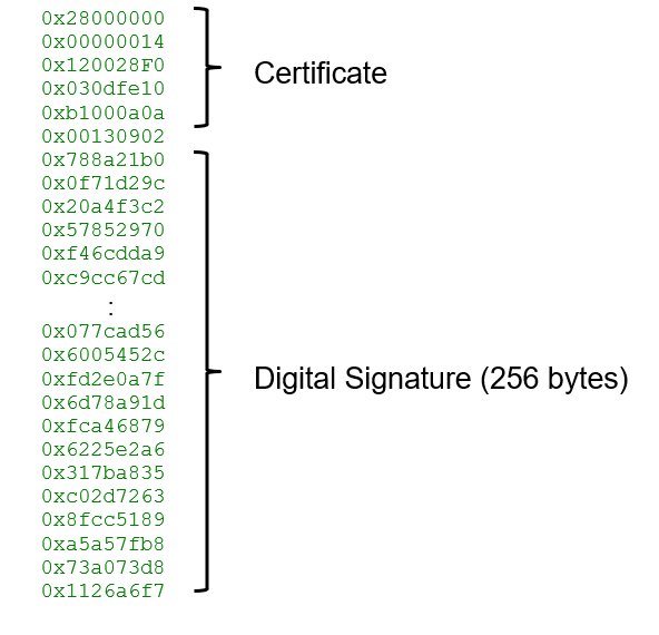
Appendix F - Configure application protection
This project provides a means of configuring Application Protection. This section describes how you can configure and add SWPU, which is Application Protection for the customer system. SWPU consists of FWPU, ERPU, and EWPU. Application Protection can be configured with up to 16 entries for FWPU and up to 4 entries for ERPU and EWPU.
Each SWPU has master/slave structure, that is, it protects the protection structure by protection structure. The slave attribute indicates access attribute to resources and the master protection attribute indicates access attribute to slave. Therefore, changes in the SWPU slave attribute requires master-defined attributes.
Application protection consists of the following elements. See the “Protection Unit” chapter in the architecture TRM [2] for more details.
PU_OBJECT_SIZE: Number of configured elements. (4 bytes)N_FWPU: Number of FWPU objects. FWPU has up to 16 regions. (4 bytes)FWPUx_SL_ADDR: Configures the FWPUx base address. (4 bytes)FWPUx_SL_SIZE: Configures the FWPUx region size and FWPUx enable. (4 bytes)FWPUx_SL_ATT: Configures the FWPUx slave attribute. (4 bytes)FWPUx_MS_ATT: Configures the FWPUx master attribute. (4 bytes)N_ERPU: Number of ERPU objects. ERPU has up to 4 regions. (4 bytes)ERPUy_SL_OFFSET: Configures the ERPUy base address offset. (4 bytes)ERPUy_SL_SIZE: Configures the ERPUy region size and ERPUy enable. (4 bytes)ERPUy_SL_ATT: Configures the ERPUy slave attribute. (4 bytes)ERPUy_MS_ATT: Configures the ERPUy master attribute. (4 bytes)N_EWPU: Number of EWPU objects. EWPU has up to 4 regions. (4 bytes)EWPUy_SL_OFFSET: Configures the EWPUy base address offset. (4 bytes)EWPUy_SL_SIZE: Configures the EWPUy region size and ERPUy enable. (4 bytes)EWPUy_SL_ATT: Configures the EWPUy slave attribute. (4 bytes)EWPUy_MS_ATT: Configures the EWPUy master attribute. (4 bytes)
Suffix “x” indicates 0 to 15, and suffix “y” indicates 0 to 3.
Configuration
The following shows the steps to configure application protection. This section address must match the "Address of Application Protection (offset = 0x108)" in TOC2. To ensure security, do not change the default value (0x17007600).
- Set the number of regions for each SWPU.
        // deification of application protection

    #define N_FWPU (0UL) /**< Number of flash write protection Max 16 \*/
    #define N_ERPU (1UL) /**< Number of efuse read protection Max 4 _/
    #define N_EWPU (1UL) /\*\*< Number of efuse write protection Max 4 _/
- Configure each SWPU according to the number of SWPUs.
         /***************************************

    - Application Protection
      ******************\*\*\*******************/

    CY_SECTION(".cy_SFlash_app_prot") \_\_USED static const cy_stc_si_app_prot_t cy_si_appprot =
    {
    .objSize = OBJECT_SIZE, /_ Application Protection Object Size (in bytes) _/
    .n_fwpu = N_FWPU, /_ Number of FWPU Max 16 _/
    .fwpu0_adr.addr30 = 0x10000000>>2ul, /_ Add region if you need _/
    .fwpu0_size.region_size = 0x200, /_ in bytes (multiple of 4) _/
    .fwpu0_size.enable = APP_PROT_ENABLE, /_ FWPU0 enable _/
    .fwpu0_sl_att.urw = APP_PROT_ALLOW, /_ FWPU0 Slave Attribute _/
    .fwpu0_sl_att.prw = APP_PROT_ALLOW, /_ FWPU0 Slave Attribute _/
    .fwpu0_sl_att.ns = APP_PROT_ALLOW, /_ FWPU0 Slave Attribute _/
    .fwpu0_sl_att.pc_mask = 0x00FF, /_ FWPU0 Slave Attribute _/
    .fwpu0_ms_att.urw = APP_PROT_ALLOW, /_ FWPU0 Master Attribute _/
    .fwpu0_ms_att.prw = APP_PROT_ALLOW, /_ FWPU0 Master Attribute _/
    .fwpu0_ms_att.ns = APP_PROT_ALLOW, /_ FWPU0 Master Attribute _/
    .fwpu0_ms_att.pc_mask = 0x00FF, /_ FWPU0 Master Attribute _/
    .n_erpu = N_ERPU, /_ Number of ERPU Max 4 _/
    .erpu0_offset.offset = 0x68, /_ ERPU0 offset (Default) _/
    .erpu0_size.region_size = 0x18, /_ ERPU0 region size (Default) _/
    .erpu0_size.enable = APP_PROT_ENABLE, /_ ERPU0 enable (Default) _/
    .erpu0_sl_att.urw = APP_PROT_ALLOW, /_ ERPU0 Slave Attribute (Default) _/
    .erpu0_sl_att.prw = APP_PROT_ALLOW, /_ ERPU0 Slave Attribute (Default) _/
    .erpu0_sl_att.ns = APP_PROT_ALLOW, /_ ERPU0 Slave Attribute (Default) _/
    .erpu0_sl_att.pc_mask = 0x00FF, /_ ERPU0 Slave Attribute (Default) _/
    .erpu0_ms_att.urw = APP_PROT_ALLOW, /_ ERPU0 Master Attribute (Default) _/
    .erpu0_ms_att.prw = APP_PROT_ALLOW, /_ ERPU0 Master Attribute (Default) _/
    .erpu0_ms_att.ns = APP_PROT_ALLOW, /_ ERPU0 Master Attribute (Default) _/
    .erpu0_ms_att.pc_mask = 0x00FF, /_ ERPU0 Master Attribute (Default) _/
    .n_ewpu = N_EWPU, /_ Number of EWPU Max 4 _/
    .ewpu0_offset.offset = 0x68, /_ EWPU0 offset (Default) _/
    .ewpu0_size.region_size = 0x18, /_ EWPU0 region size (Default) _/
    .ewpu0_size.enable = APP_PROT_ENABLE, /_ EWPU0 enable (Default) _/
    .ewpu0_sl_att.urw = APP_PROT_ALLOW, /_ EWPU0 Slave Attribute (Default) _/
    .ewpu0_sl_att.prw = APP_PROT_ALLOW, /_ EWPU0 Slave Attribute (Default) _/
    .ewpu0_sl_att.ns = APP_PROT_ALLOW, /_ EWPU0 Slave Attribute (Default) _/
    .ewpu0_sl_att.pc_mask = 0x00FF, /_ EWPU0 Slave Attribute (Default) _/
    .ewpu0_ms_att.urw = APP_PROT_ALLOW, /_ EWPU0 Master Attribute (Default) _/
    .ewpu0_ms_att.prw = APP_PROT_ALLOW, /_ EWPU0 Master Attribute (Default) _/
    .ewpu0_ms_att.ns = APP_PROT_ALLOW, /_ EWPU0 Master Attribute (Default) _/
    .ewpu0_ms_att.pc_mask = 0x00FF, /_ EWPU0 Master Attribute (Default) _/
    };
Table 10 shows details for each element.
Table 10. Elements descriptions
Element | Description |
|---|---|
.objeSize | Number of configured elements |
.n_fwpu | Number of FWPUs |
.n_erpu | Number of ERPUs |
.n_ewpu | Number of EWPUs |
.fwpu0_adr.addr30 | Base address of FWPU0. 4-byte aligned. |
.fwpu0_size.region_size | FWPU0 region size |
.fwpu0_size.enable | FWPU0 enable. 0: Disable 1: Enable |
.fwpu0/erpu0/ewpu0_sl_att.urw | FWPU0/EWPU0 slave attribute for user write restriction. 0: Prohibit 1: Allow EWPU0 slave attribute for user read restriction. 0: Prohibit 1: Allow |
.fwpu0/erpu0/ewpu0_sl_att.prw | FWPU0/EWPU0 slave attribute for privileged write restriction. 0: Prohibit 1: Allow EWPU0 slave attribute for privileged read restriction. 0: Prohibit 1: Allow |
.fwpu0/erpu0/ewpu0_sl_att.ns | FWPU0/EWPU0 slave attribute for non-secure write restriction. 0: Prohibit 1: Allow EWPU0 slave attribute for non-secure read restriction. 0: Prohibit 1: Allow |
.fwpu0/erpu0/ewpu0_sl_att.pc_mask | FWPU0/ERPU0/EWPU0 slave attribute for PC restriction. The PC number corresponds to the bit number. 0: Prohibit 1: Allow (When pc_mask is 0x0005, PC0, and PC2 are allowed) |
.fwpu0_ms_att.urw | FWPU0/EWPU0 master attribute for user write restriction. 0: Prohibit 1: Allow EWPU0 master attribute for user read restriction. 0: Prohibit 1: Allow |
.fwpu0_ms_att.prw | FWPU0/EWPU0 master attribute for privileged write restriction. 0: Prohibit 1: Allow EWPU0 master attribute for privileged read restriction. 0: Prohibit 1: Allow |
.fwpu0_ms_att.ns | FWPU0/EWPU0 master attribute for non-secure write restriction. 0: Prohibit 1: Allow EWPU0 master attribute for non-secure read restriction. 0: Prohibit 1: Allow |
.fwpu0_ms_att.pc_mask | FWPU0/ERPU0/EWPU0 master attribute for PC restriction. The PC number corresponds to the bit number. 0: Prohibit 1: Allow (When pc_mask is 0x0005, PC0 and PC2 are allowed) |
.erpu0/ewpu0_offset.offset | ERPU0 base address offset |
.erpu0/ewpu0_size.region_size | ERPU0 region size |
.erpu0/ewpu0_size.enable | ERPU0 enable. 0: Disable 1: Enable |
Appendix G - Normal access restriction
This project provides a configuration of the Normal Access Restriction (NAR). NAR determines DAP restrictions for NORMAL_PROVISIONED and SECURE_W_DEBUG. NAR is deployed in flash booting. See the “BootROM” chapter in the architecture TRM [2] and Security enhance PPU configuration.
This project can configure the Normal Access Restrictions and Normal Dead Access Restrictions for M0+ DAP, M4 DAP, and System DAP.
Configuration
The following code shows the steps to configure normal access restriction. This section is located at 0x17001A00 in SFlash.
             #define CY_SI_CM0_ENABLE                (0UL)  /**< CM0 ACCESS PORT ENABLE */
             #define CY_SI_CM0_DISABLE_TMP           (1UL)  /**< CM0 ACCESS PORT TEMPORARY DISABLE */
             #define CY_SI_CM0_DISABLE               (2UL)  /**< CM0 ACCESS PORT PERMANENTLY_DISABLE */
             #define CY_SI_CM4_ENABLE                (0UL)  /**< CM4 ACCESS PORT ENABLE */
             #define CY_SI_CM4_DISABLE_TMP           (1UL)  /**< CM4 ACCESS PORT TEMPORARY DISABLE */
             #define CY_SI_CM4_DISABLE               (2UL)  /**< CM4 ACCESS PORT PERMANENTLY_DISABLE */
             #define CY_SI_SYS_ENABLE                (0UL)  /**< SYS ACCESS PORT ENABLE */
             #define CY_SI_SYS_DISABLE_TMP           (1UL)  /**< SYS ACCESS PORT TEMPORARY DISABLE */
             #define CY_SI_SYS_DISABLE               (2UL)  /**< SYS ACCESS PORT PERMANENTLY_DISABLE */


             /* Access Restriction */
             #define CY_SI_NAR_NORMALACCESSRESTRICTION ((CY_SI_CM0_ENABLE << CY_SI_CM0_AP_POS) \
                                    | (CY_SI_CM4_ENABLE << CY_SI_CM4_AP_POS) \
                                    | (CY_SI_SYS_ENABLE << CY_SI_SYS_AP_POS)) \
                                    | 0x80                                               /* Fixed value */

             #define CY_SI_NAR_NORMALDEADACCESSRESTRICTION ((CY_SI_CM0_ENABLE << CY_SI_CM0_AP_POS) \
                                    | (CY_SI_CM4_ENABLE << CY_SI_CM4_AP_POS) \
                                    | (CY_SI_SYS_ENABLE << CY_SI_SYS_AP_POS))

             CY_SECTION(".cy_SFlash_nar") __USED static const cy_stc_si_nar_t cy_nar =
             {
        .nar         = CY_SI_NAR_NORMALACCESSRESTRICTION,       /* Normal Access Restrictions */
        .ndar        = CY_SI_NAR_NORMALDEADACCESSRESTRICTION,   /* Normal Dead Access Restrictions */
             };
Table 11 shows details for each element.
Table 11. NAR setting
Element | Description |
|---|---|
CY_SI_CM0/CM4/SYS_ENABLE | Set to Enable M0/M4/SYS-DAP. |
CY_SI_CM0/CM4/SYS_DISABLE_TMP | Set to Disable M0/M4/SYS-DAP. |
CY_SI_CM0/CM4/SYS_DISABLE | Set to Permanently Disable M0/M4/SYS-DAP. |
See Table 5 for setting details.
Appendix H - Example programs and scripts
The sample project has the following sample programs and scripts. The sample programs and scripts shown here use the CYT2B7 series. Also, GHS MULTI is used to execute the script.
Sample code
The sample project has the following sample programs:
- Debug Access Port Authentication
- TransitiontoSecure API Execution
- ReadUniqueID API Execution
- TransitiontoRMA API Execution
- OpenRMA API Execution
Debug access port authentication
In this sample program, when powered, the boot starts by disabling all DAPs. CM0+ configures Sys_DAP MPU and enables Sys_DAP. Then, the MCU accepts the specific 128-bit key from Sys_DAP, and the 128-bits key is compared with the 128-bit key stored in the MCU in advance. If they match, CM0+_DAP and CM4_DAP are enabled. The following is an overview of this sample program.
- CM0+ handles DAP restrictions
- NAR setting
- AP_CTL_M0_DISABLE: 1 (= Disable)
- AP_CTL_M4_DISABLE: 1 (= Disable)
- AP_CTL_SYS_DISABLE: 1 (= Disable)
- SYS_AP_MPU_ENABLE: 0 (= Disable)
- Sys_DAP MPU configuration
- Region 0: Background Region
- Base Address: 0x00000000
- Subregion: 0x00
- Size: 4 GB
- Attribute: No Access, Secure
- Region 1: MMIO Region (Only IPC channel structure 0/1/2)
- Base Address: 0x40220000
- Subregion: 0xf8
- Size: 256 bytes
- Attribute: All Access, Non-Secure
- Region 6: SRAM Region (0x08001000 to 0x08003FFF)
- Base Address: 0x08000000
- Subregion: 0x03 (First 4 KB of SRAM is disabled)
- Size: 16 Kbytes
- Attribute: All access, Non-Secure
- Region 0: Background Region
- 128-bits key is stored to Work Flash (Address = 0x14012000)
- The parameters (including 128-bits key) input from the Sys_DAP is passed via IPC2. Figure 14 shows the parameters structure.
Figure 14. Parameters structure

These parameters are input via Sys-DAP from GHS MULTI using script:
- IPC2 generates notify interrupt to CM0+ when parameters are ready.
- IPC2 notify interrupt is mapped to IRQ3 (Priority 3).
Figure 15 shows interrupt connection for this sample program.
Figure 15. Interrupt connection

Note: In CYT2B series, IPC channel 2 is reserved for Sys_DAP. IPC channel 2 is the IPC channel number assigned to launch the API from Sys_DAP. See the architecture TRM [2] for IPC channels assigned by the product.
Operation flow
Figure 16 shows software flow of this sample program.
Figure 16. Software flow for DAP authentication

- CM0+ activates CM4.
- CM0+ configures initial setting
- CM0+ configures IPC2 and interrupt controller.
- CM0+ configures SWD/JTAG pin
- CM0+ configures Sys_DAP MPU
- Enable Sys_DAP
- Write SRAM_SCRATCH address to IPC2.DATA0 register from Sys_DAP
- Write Code and Key data to SRAM_SCRATCH address from Sys_DAP
- Set IPC2.Notify to generate interrupt.
- When CM0+ accepts the interrupt, it reads SRAM_SCRATCH address from IPC2.DATA0.
- Read the code from SRAM_SCRATCH address.
- Check if Code is 0x55000000. If it is not 0x55000000, set 0xCC000000 to Status Code and return from interrupt handler.
- Read Key (Key_0) in Work Flash.
- Read Key (Key_1) in SRAM_SCRATCH address.
- Compare Key_0 and Key1. If they do not match, set 0xFF000000 to Status Code and return from interrupt handler.
- Enable the CM0+_DAP and CM4_DAP, when Key_0 and Key1 match.
- Set 0xAA000000 to Status Code, and return from interrupt handler.
- Check the status code.
- If Status code is set to 0xAA000000, AP enabling was successful. If Status code is set to 0xCC000000 or 0xFF000000, DAP enabling was failed.
Note: This is only an example and you must decide on the code allocation to individual CPUs based on your security requirements.
Configuration
Here are the steps to configure DAP authentication. These code snippets and scripts are available in: \tviibe1m\src\DAP_restrict
Sample project stored folder
- Configure the Key Data.
Set the Key Data to Work Flash to be compared with 128-bit key entered from Sys_DAP.
        uint8_t  programData[SIZE_128_BIT_IN_BYTE] = {     --> Key Data in Work Flash
    0x33, 0x22, 0x11, 0x00,                            --> Key Data 1
    0x77, 0x66, 0x55, 0x44,                            --> Key Data 2
    0xbb, 0xaa, 0x99, 0x88,                            --> Key Data 3
    0xff, 0xee, 0xdd, 0xcc,                            --> Key Data 4
    };
- Configure NAR.
Configure NAR according to the system.
        /* Access Restriction */
    /* CY_SI_DIRECT_EXE_DISABLE in CY_SI_NAR_NORMALACCESSRESTRICTION is fixed value */
    #define CY_SI_NAR_NORMALACCESSRESTRICTION ((CY_SI_CM0_DISABLE_TMP << CY_SI_CM0_AP_POS) \
                                             | (CY_SI_CM4_DISABLE_TMP << CY_SI_CM4_AP_POS) \
                                             | (CY_SI_SYS_DISABLE_TMP << CY_SI_SYS_AP_POS) \
                                             | (CY_SI_MPU_DISABLE << CY_SI_AP_MPU_POS)\
                                             | (CY_SI_DIRECT_EXE_DISABLE << CY_SI_DIRECT_EXECUTE_POS) \
                                             | (CY_SI_FLASH_ ENABLE << CY_SI_FLASH_POS) \
                                             | (CY_SI_RAM0_ENABLE << CY_SI_RAM0_POS) \
                                             | (CY_SI_WORK_FLASH_ ENABLE << CY_SI_WORK_FLASH_POS) \
                                             | (CY_SI_SFLASH_ENABLE << CY_SI_SFLASH_POS) \
                                             | (CY_SI_MMIO_ENABLE << CY_SI_MMIO_POS))
This setting disables all DAPs. Sys_DAP MPU is set by the application software.
Note: It is recommended to disable DAPs after programming the application software for CM0+ and CM4. Otherwise, the application software may not be programmed.
- Configure the SRAM_SCRATCH parameters.
Create the data to write to SRAM as parameters. These parameters are created as text data.
        0x55000000               --> Code
    0x00112233               --> Key Data 1
    0x44556677               --> Key Data 2
    0x8899aabb               --> Key Data 3
    0xccddeeff               --> Key Data 4
-
Execute.
-
Copy the script file to \ tviibe1m\tools\ghs.
-
Input the following command in the Command pane of the GHS MULTI debug window.
MULTI> python OpenDAP.py [file name] [SRAM_SCRATCH Address]
-
Where,
[file name] is the file in which the Code and Key are written.
[SRAM_SCRATCH Address] must indicate a valid area.
TransitiontoSecure API execution
This API transitions the lifecycle stage of the MCU to “SECURE” or "SECURE_W_DEBUG". This API validates the FACTORY_HASH, and programs the SECURE_HASH, secure access restrictions, and dead access restrictions into eFuse.
Execution of this API requires that the MCU lifecycle stage is in “NORMAL_PROVISIONED”. In addition, note that an MCU cannot return to “NORMAL_PROVISIONED” lifecycle stage after the transition of lifecycle stage to “SECURE” or “SECURE_W_DEBUG”.
Note: When transitioning to SECURE or SECURE_W_DEBUG lifecycle stage, it is recommended to call with the ROM boot default clock configuration settings. See the Blow Fuse Bit in the architecture TRM [2] for more details.
Sample program
This sample code is available in: \tviibe1m\src\APIs_usage
Sample project stored folder
This API has the following parameters, and runs from CM0+.
Parameter setting for transition to SECURE:
    #define SECURE                  (0x0ul)
    #define SECURE_ACC_RESTRICT     (0x00000000ul) // For SECURE
    #define DEAD_ACC_RESTRICT       (0x00000000ul) // For SECURE
Parameter setting for transition to SECURE_W_DEBUG
    #define SECURE_WITH_DEBUG       (0x1ul)
    #define SECURE_WD_ACC_RESTRICT  (0x00000080ul) // For SECURE WITH DEBUG
    #define DEAD_WD_ACC_RESTRICT    (0x00000000ul) // For SECURE WITH DEBUG
Script
This script is available in: \tviibe1m\tools\ghs\Script
Sample project stored folder
The following is the execution procedure:
-
Copy the script file to \tviibe1m\tools\ghs
-
Input the following command in the Command pane of the GHS MULTI debug window.
MULTI> python TransitionToSecure.py(/TransitionToSecure_with_Debug.py) [SECURE_ACCESS_RESTRICT] [DEAD_ACCESS_RESTRICT] [SRAM_SCRATCH Address]
ReadUniqueID API execution
This API reads the unique ID of the die from SFlash. The unique ID is used for RMA lifecycle stage transition.
Sample program
This sample code is available in:\tviibe1m\src\APIs_usage>\tviibe1m\src\APIs_usage
Sample project stored folder
Unique ID is returned to SRAM_SCRACH after running this API. This API runs from CM4.
SRAM_SCRATCH address | Bits [31:28] | Bits [23:16] | Bits [15:8] | Bits [7:0] |
|---|---|---|---|---|
0x00 | Status Code 0xA0: Success, 0xF0: Error | Unique ID_0 | ||
0x04 | Unique ID_1 | |||
0x08 | Unique ID_2 | |||
Script
This script is available in: \tviibe1m\tools\ghs\Script
Sample project stored folder
The following is the execution procedure:
-
Copy the script file to \tviibe1m\tools\ghs.
-
Input the following command in the Command pane of the GHS MULTI debug window:
MULTI> python ReadUniqueID.py [SRAM_SCRATCH Address]
-
Read the UniqueID:
MULTI> target t 0 mr 4 [SRAM_SCRATCH Address]
MULTI> target t 0 mr 4 [SRAM_SCRATCH Address+4] MULTI> target t 0 mr 4 [SRAM_SCRATCH Address+8]
TransitiontoRMA API execution
This API transitions the lifecycle stage of the MCU to “RMA”. The TransitiontoRMA API converts parts from SECURE, or SECURE_W_DEBUG to the RMA lifecycle stage. RMA lifecycle stage parts can be opened for analysis by running the OpenRMA API. In addition, the valid public key must be stored in SFlash.
Sample program
This sample code is available in: \tviibe1m\src\APIs_usage
Sample project stored folder
This API has the following parameters, and runs from CM0+. These parameters show an example of RSA-2048:
Parameter setting for Transition to RMA.
    // Transition To RMA and Open RMA parameters
    #define OBJECT_SIZE_TRANSITION_TO_RAM  (0x00000014ul)
    #define COMMND_ID_TRAN_TO_RMA          (0x120028F0ul)
    #define UNIQUE_ID_0                    (0x028992f2ul) // Need to change per chip
    #define UNIQUE_ID_1                    (0xb3000101ul) // Need to change per chip
    #define UNIQUE_ID_2                    (0x00140708ul) // Need to change per chip

    uint32_t Digital_Signature_TransitionToRMA[64]
    =  {0x5c1bbb5dul, 0xc6bae36dul, 0xe48c4044ul, 0xf8dd8131ul, 0x57230ea4ul, 0x4ede3ce5ul, 0xba0b8960ul, 0x5cb4d66ful,
         0x2362e0b7ul, 0x88e6a3f1ul, 0x353caae9ul, 0xf8630ad6ul, 0x2f388ca7ul, 0x9ee16a77ul, 0xce92ec23ul, 0xec16037aul,
         0x00c3b4feul, 0x891409fcul, 0xe0242d69ul, 0xa00b6018ul, 0x2e677254ul, 0x4d64188bul, 0xcef8a86dul, 0x03a0fdf6ul,
         0xf4b511b6ul, 0x123a3df3ul, 0x19f41b52ul, 0xecbad2a7ul, 0x43e3a1cbul, 0xe1ec4fecul, 0xd6c78392ul, 0x63de12b8ul,
         0x1a1f08aaul, 0xd3cdf2a8ul, 0xf0430eb9ul, 0x109decfbul, 0x22a05b23ul, 0x9a3d8181ul, 0x0f4c4f1ful, 0x1c62a64cul,
         0xed971c41ul, 0x57e74366ul, 0x991cb9a4ul, 0xfa8e4bfeul, 0x19ed9cccul, 0xd2fd7e5eul, 0xd517af36ul, 0x66679d89ul,
         0x004ec3f4ul, 0xafcbf55eul, 0xaf0a4a85ul, 0xb09f362cul, 0x7b7abe4aul, 0x626e826dul, 0x56511b05ul, 0x7089b60eul,
         0xe15cac61ul, 0x83bd7290ul, 0x45beac77ul, 0x1eb7d67aul, 0xc886dc0bul, 0x05736051ul, 0xf8105b97ul, 0x680a5d41ul,};
Note: See Requirements for transition to RMA lifecycle stage for conditions TransitiontoRMA API execution.
Script
This script is available in: \tviibe1m\tools\ghs\Script
Sample project stored folder
The following is the execution procedure:
-
Create the certificate and digital signature. See Appendix E - Transition to RMA lifecycle stage for certificate and digital signature generation of TransitiontoRMA API.
-
Copy the script file to \ tviibe1m\tools\ghs
-
Input the following command in the Command pane of the GHS MULTI debug window.
MULTI> python TransitionRMA.py [file name] [SRAM_SCRATCH Address] [DIGITAL_SIGNATURE Address]
Where,
[file name] is the file in which the certificate and digital signature for TransitiontoRMA API are written.
Note: See Requirements for transition to RMA lifecycle stage for the conditions to execute the TransitiontoRMA API.
Note: See Minimum requirements for a system call initiated by a debugger to run the TransitiontoRMA API from Sys_DAP.
OpenRMA API Execution
A device in the RMA lifecycle stage can be analyzed by running the OpenRMA API. The certificate and digital signature are required to run this API. In addition, the valid public key must be stored in SFlash.
Script
This script is available in: \ tviibe1m\tools\ghs\Script
Sample project stored folder
-
The following is the execution procedure: Create certificate and digital signature. See Appendix E - Transition to RMA lifecycle stage for certificate and digital signature generation of TransitiontoRMA API.
-
Copy the script file to \tviibe1m\tools\ghs
-
Input the following command in the Command pane of the GHS MULTI debug window.
MULTI> python TransitionRMA.py [file name] [SRAM_SCRATCH Address] [DIGITAL_SIGNATURE Address]
Where,
[file name] is the file in which the certificate and digital signature for OpenRMA API are written.
Note: See Requirements for transition to RMA lifecycle stage for the conditions to execute the OpenRMA API.
Running the API
In this sample project, running the API can be selected by “ExecuteAPI” in the main_cm0plus.c source file.Table 13 lists the ExecuteAPI setting and running the API.
Table 13. ExecuteAPI parameter
ExecuteAPI | Running API |
|---|---|
= 1 | TransitiontoRMA API |
= 3 | TransitiontoSecure API (for SECURE) |
= 4 | TransitiontoSecure API (for SECURE_W_DEBUG) |
Others | ReadUniqueID API (Default: 0) |
// SystemInit();
// Fault report structure setting in User Application
// Masked ECC errors for OpenRMA
// Need to select Fault report structure according to your system (Fault report Structure 0 is used as an example)
if(CPUSS->unPROTECTION.stcField.u3STATE == 1ul) {
Cy_SysFlt_ClearMaskByIdx(FAULT_STRUCT0, CY_SYSFLT_RAMC0_C_ECC); // Mask RAM0 correctable ECC violation
Cy_SysFlt_ClearMaskByIdx(FAULT_STRUCT0, CY_SYSFLT_RAMC0_NC_ECC); // Mask RAM0 non-correctable ECC violation
Cy_SysFlt_ClearMaskByIdx(FAULT_STRUCT0, CY_SYSFLT_CRYPTO_C_ECC); // Mask Crypto memory correctable ECC violation
Cy_SysFlt_ClearMaskByIdx(FAULT_STRUCT0, CY_SYSFLT_CRYPTO_NC_ECC); // Mask Crypto memory non-correctable ECC violation
}
switch (ExecuteAPI) {
case 1:
// Masked ECC errors for TransitiontoRMA
// Need to select Fault report structure according to your system (Fault report Structure 0 is used as an example)
Cy_SysFlt_ClearMaskByIdx(FAULT_STRUCT0, CY_SYSFLT_RAMC0_C_ECC); // Mask RAM0 correctable ECC violation
Cy_SysFlt_ClearMaskByIdx(FAULT_STRUCT0, CY_SYSFLT_RAMC0_NC_ECC); // Mask RAM0 non-correctable ECC violation
Cy_SysFlt_ClearMaskByIdx(FAULT_STRUCT0, CY_SYSFLT_CRYPTO_C_ECC); // Mask Crypto memory correctable ECC violation
Cy_SysFlt_ClearMaskByIdx(FAULT_STRUCT0, CY_SYSFLT_CRYPTO_NC_ECC); // Mask Crypto memory non-correctable ECC violation
params.TransitionToRMA.arg0.Opcode = OPCODE_TRANSITION_TO_RMA;
params.TransitionToRMA.arg1.Objsize = OBJECT_SIZE_TRANSITION_TO_RAM;
params.TransitionToRMA.arg2.CommandId = COMMND_ID_TRAN_TO_RMA;
params.TransitionToRMA.arg3.UniqueID_0 = UNIQUE_ID_0;
params.TransitionToRMA.arg4.UniqueID_1 = UNIQUE_ID_1;
params.TransitionToRMA.arg5.UniqueID_2 = UNIQUE_ID_2;
params.TransitionToRMA.arg6.dataAddr = (uint32_t)Digital_Signature_TransitionToRMA;
break;
case 3:
params.TransitionToSecure.arg0.Opcode = OPCODE_TRANSITION_TO_SECURE;
params.TransitionToSecure.arg0.Debug = SECURE;
params.TransitionToSecure.arg1.Acc_restrict = SECURE_ACC_RESTRICT;
params.TransitionToSecure.arg2.Dead_Acc_restrict = DEAD_ACC_RESTRICT;
break;
case 4:
params.TransitionToSecure.arg0.Opcode = OPCODE_TRANSITION_TO_SECURE;
params.TransitionToSecure.arg0.Debug = SECURE_WITH_DEBUG;
params.TransitionToSecure.arg1.Acc_restrict = SECURE_WD_ACC_RESTRICT;
params.TransitionToSecure.arg2.Dead_Acc_restrict = DEAD_WD_ACC_RESTRICT;
break;
default:
params.RdUnId.arg0.Opcode = OPCODE_READ_UNIQUEID;
break;
}
Cy_IPC_Drv_SendMsgWord(syscall_ipc_struct, CY_SROM_DR_IPC_NOTIFY_STRUCT, (uint32_t)¶ms);
First, check if the device is RMA. If the protection state is "1", that is, VIRGIN, masks ECC error fault factors. Next, if ExecuteAPI is “1”, the device runs TransitiontoRMA API. It masks ECC error fault factors also before running TransitiontoRMA API. See Requirements for transition to RMA lifecycle stage for details.
Security enhance PPU configuration example
This section shows the sample program that configures the programmable protection units, PPU11, 12, 13, and PERI_MS_PPU_FX_CPUSS_CM0 (see Figure 6), when security enhancement is valid. In a secure system, the configuration of these PPUs needs to be performed with the HSM software.
Figure 17 shows the software flow of this sample program.
Figure 17. Protection unit configuration for security enhancement

The following configuration is performed by CM0+ (HSM software).
- Set CM0+ PC_MASK to “2”. CM0+ can set PC=”2” only.
- Set CM4 PC_MASK to “3” to “7”. CM4 can set PC=”3” to “7”.
- Set CM0+ PC to “2”. The HSM software uses PC=”2”.
- Set CM4 PC to “3”. The application software uses PC=”3”.
- Configure protection units. (1)
- Activate CM4.
The following configuration is performed by CM4.
- Perform ECC logic test.
- Configure protection unit. (2)
Table 14 shows the PPU configuration performed by each CPU.
Table 14. Protection unit configuration
Name of PPU | Configure protection units (1) by CM0+ (Master/Slave) | Configure protection units (2) by CM4 (Master/Slave) |
|---|---|---|
Programmable PPU 11 | PC3: Read / Write PC1, 2, 4-7: Read only | |
Programmable PPU 12 | PC2, 3: Read / Write PC1, 4-7: Read only | PC2: Read / Write PC1, 3-7: Read only |
Programmable PPU 13 | PC3: Read / Write PC1, 2, 4-7: Read only | |
PERI_MS_PPU_FX_CPUSS_CM0 (PPU index=17) | PC2: Read / Write PC1, 3-7: Read only |
Table 15 lists the parameters and Table 16 lists the functions in SDL for protection unit configuration.
Table 15. List of setting parameters
Parameters | Description | Value |
|---|---|---|
CY_SECURITY_ENHANCED | Security Enhancement marker | 0xFEDEEDDF |
CY_PROT_PC2 to PC7 | Protection context value | 2u to 7u |
PC_MASK_OF_PC2 to PC7 | Protection context mask value | x = 2 to 7 |
CY_PROT_PERM_R | Read only attribute | 0x01u |
CY_PROT_PERM_RW | Read / Write attribute | 0x03u |
CPUSS_MS_ID_CM0 | CM0+ Bus muster ID | 0 |
CPUSS_MS_ID_CM4 | CM4 Bus muster ID | 14 |
PERI_MS_PPU_PR11 | Programmable PPU#11 base address | 0x400102C0 |
PERI_MS_PPU_PR12 | Programmable PPU#12 base address | 0x40010300 |
PERI_MS_PPU_PR13 | Programmable PPU#13 base address | 0x40010340 |
PERI_MS_PPU_FX_CPUSS_CM0 | PERI_MS_PPU_FX_CPUSS_CM0 PPU base address | 0x40010C40 |
ppuFixedAttr_ReadOnly.userPermission | Fixed PPU user attribute for read only | CY_PROT_PERM_R |
ppuFixedAttr_ReadOnly.privPermission | Fixed PPU privileged attribute for read only | CY_PROT_PERM_R |
ppuFixedAttr_ReadOnly.secure | Fixed PPU secure attribute for read only | 0ul |
ppuFixedAttr_Readwrite.userPermission | Fixed PPU user attribute for read/write | CY_PROT_PERM_RW |
ppuFixedAttr_Readwrite.privPermission | Fixed PPU privileged attribute for read/write | CY_PROT_PERM_RW |
ppuFixedAttr_Readwrite.secure | Fixed PPU secure attribute for read/write | 0ul |
ppuProgAttr_ReadOnly.userPermission | Programmable PPU user attribute for read only | CY_PROT_PERM_R |
ppuProgAttr_ReadOnly.privPermission | Programmable PPU privileged attribute for read only | CY_PROT_PERM_R |
ppuProgAttr_ReadOnly.secure | Programmable PPU secure attribute for read only | 0ul |
ppuProgAttr_Readwrite.userPermission | Programmable PPU user attribute for read/write | CY_PROT_PERM_RW |
ppuProgAttr_Readwrite.privPermission | Programmable PPU privileged attribute for read/write | CY_PROT_PERM_RW |
ppuProgAttr_Readwrite.secure | Programmable PPU secure attribute for read/write | 0ul |
Table 16. List of protection configuration functions
Function | Description | Note |
|---|---|---|
Cy_Prot_ConfigBusMaster (busMaster, privileged, secure, pcMask) | Protection context mask setting | |
Cy_Prot_SetActivePC(busMaster, pc) | Protection context setting | |
Init_ProtectionUnit_Secure_Enahnce() | Protection unit configuration (1) | |
Cy_Prot_ConfigPpuProgSlaveStructAttr(base, setPC, config) | Programmable PPU slave configuration | |
Cy_Prot_ConfigPpuProgMasterStructAttr (base, setPC, config) | Programmable PPU master configuration | |
Cy_Prot_ConfigPpuFixedSlaveStruct (base, setPC, config) | Fixed PPU slave configuration | |
Cy_Prot_ConfigPpuFixedMasterStruct (base, setPC, config) | Fixed PPU master configuration | |
Invalidate_ProtectionUnit_PPU12() | Protection unit configuration (2) |
The following description will help you understand the register notation of the SDL driver:
-
addrMpu->unMS_CTL.u32Register is the PROT_MPUx_MS_CTL register mentioned in the registers TRM [2]. Other registers are also described in the same manner. “x” signifies the bus master identifiers.
-
Performance improvement measures
-
To improve the performance of register setting, the SDL writes a complete 32-bit data to the register. Each bit field is generated in advance in a bit-writable buffer and written to the register as the final 32-bit data.
tempSL_ATT0.u32Register = base->unSL_ATT0.u32Register; tempSL_ATT0.stcField.u1PC1_UR = (config->userPermission & CY_PROT_PERM_R); tempSL_ATT0.stcField.u1PC1_UW = (config->userPermission & CY_PROT_PERM_W) >> 1; tempSL_ATT0.stcField.u1PC1_PR = (config->privPermission & CY_PROT_PERM_R); tempSL_ATT0.stcField.u1PC1_PW = (config->privPermission & CY_PROT_PERM_W) >> 1; tempSL_ATT0.stcField.u1PC1_NS = !(config->secure); base->unSL_ATT0.u32Register = tempSL_ATT0.u32Register;
See Code Listing 1 to Code Listing 10 for sample codes of the protection unit configuration.
Code Listing 1 Protection unit configuration (CM0+)
    CY_SECTION(".cy_toc_part2") __USED static const cy_stc_si_toc_t cy_toc2 =
    {
    :
       /*  Set Security marker to valid  */
    .securityMarker = CY_SECURITY_ENHANCED,          /* Offset+0xFC Security Enhance Marker */
    :
    };

    /******************************************************************************/
    /* Programmable PPU11, 12, 13, and FixePPU 17 Configuration */
    /******************************************************************************/
    #define PC_MASK_OF_PC2 (1u<<(CY_PROT_PC2-1u))   /*  Define PC_MASK value  */
    #define PC_MASK_OF_PC3 (1u<<(CY_PROT_PC3-1u))
    #define PC_MASK_OF_PC4 (1u<<(CY_PROT_PC4-1u))
    #define PC_MASK_OF_PC5 (1u<<(CY_PROT_PC5-1u))
    #define PC_MASK_OF_PC6 (1u<<(CY_PROT_PC6-1u))
    #define PC_MASK_OF_PC7 (1u<<(CY_PROT_PC7-1u))

    const cy_stc_ppu_gr_cfg_t  ppuFixedAttr_ReadOnly =   /*  Fixed PPU attribute (Read only)  */
    {
        .userPermission = CY_PROT_PERM_R,
        .privPermission = CY_PROT_PERM_R,
        .secure         = 0ul,
    };
    const cy_stc_ppu_gr_cfg_t  ppuFixedAttr_Readwrite =   /*  Fixed PPU attribute (Read/Write)   */
    {
        .userPermission = CY_PROT_PERM_RW,
        .privPermission = CY_PROT_PERM_RW,
        .secure         = 0ul,
    };
    const cy_stc_ppu_prog_attr_cfg_t  ppuProgAttr_ReadOnly =   /*  Programmable PPU attribute (Read only)   */
    {
        .userPermission = CY_PROT_PERM_R,
        .privPermission = CY_PROT_PERM_R,
        .secure         = 0ul,
    };
    const cy_stc_ppu_prog_attr_cfg_t  ppuProgAttr_Readwrite =   /*  Programmable PPU attribute (Read/Write)   */
    {
        .userPermission = CY_PROT_PERM_RW,
        .privPermission = CY_PROT_PERM_RW,
        .secure         = 0ul,
    };

    int main(void)
    {
    :
    /* Protection Context Setting HSM(CM0+) = PC2, Application(CM4) = PC3-7 */
    Cy_Prot_ConfigBusMaster(CPUSS_MS_ID_CM0, true, true, PC_MASK_OF_PC2);   /*  (1)CM0+ PC_MASK setting   */
       /*  (2)CM4 PC_MASK setting   */
    Cy_Prot_ConfigBusMaster(CPUSS_MS_ID_CM4, true, true, (PC_MASK_OF_PC3|PC_MASK_OF_PC4|PC_MASK_OF_PC5|PC_MASK_OF_PC6|PC_MASK_OF_PC7));


    Cy_Prot_SetActivePC(CPUSS_MS_ID_CM0, CY_PROT_PC2);   /*  (3)CM0+ PC setting   */
    Cy_Prot_SetActivePC(CPUSS_MS_ID_CM4, CY_PROT_PC3);    /*  (4)CM4 PC setting   */

    Init_ProtectionUnit_Secure_Enahnce();   /*  (5)Configure protection unit. See [Code Listing 2](#code-listing-2-init_protectionunit_secure_enahnce).  */
    :

    Cy_SysEnableApplCore(CY_CORTEX_M4_APPL_ADDR);   /*  (6)Activate CM4  */

    while(1)
        {
        }
    }
Code Listing 2 Init_ProtectionUnit_Secure_Enahnce()
    void Init_ProtectionUnit_Secure_Enahnce(void)
    {


    // Programmable PPU11 Slave structure(PC1-7) Setting
       /*  Configure slave programmable PPU#11. (Slave) See Code Listing 7.  */
    Cy_Prot_ConfigPpuProgSlaveStructAttr(PERI_MS_PPU_PR11, CY_PROT_PC1, &ppuProgAttr_ReadOnly);
    Cy_Prot_ConfigPpuProgSlaveStructAttr(PERI_MS_PPU_PR11, CY_PROT_PC3, &ppuProgAttr_Readwrite);
    Cy_Prot_ConfigPpuProgSlaveStructAttr(PERI_MS_PPU_PR11, CY_PROT_PC4, &ppuProgAttr_ReadOnly);
    Cy_Prot_ConfigPpuProgSlaveStructAttr(PERI_MS_PPU_PR11, CY_PROT_PC5, &ppuProgAttr_ReadOnly);
    Cy_Prot_ConfigPpuProgSlaveStructAttr(PERI_MS_PPU_PR11, CY_PROT_PC6, &ppuProgAttr_ReadOnly);
    Cy_Prot_ConfigPpuProgSlaveStructAttr(PERI_MS_PPU_PR11, CY_PROT_PC7, &ppuProgAttr_ReadOnly);
    // Set the current PC last
    Cy_Prot_ConfigPpuProgSlaveStructAttr(PERI_MS_PPU_PR11, CY_PROT_PC2, &ppuProgAttr_ReadOnly);


    // Programmable PPU11 Master structure(PC1-7) Setting
       /*  Configure programmable PPU#11. (Master) See Code Listing 8.  */
    Cy_Prot_ConfigPpuProgMasterStructAttr(PERI_MS_PPU_PR11, CY_PROT_PC1, &ppuProgAttr_ReadOnly);
    Cy_Prot_ConfigPpuProgMasterStructAttr(PERI_MS_PPU_PR11, CY_PROT_PC3, &ppuProgAttr_Readwrite);
    Cy_Prot_ConfigPpuProgMasterStructAttr(PERI_MS_PPU_PR11, CY_PROT_PC4, &ppuProgAttr_ReadOnly);
    Cy_Prot_ConfigPpuProgMasterStructAttr(PERI_MS_PPU_PR11, CY_PROT_PC5, &ppuProgAttr_ReadOnly);
    Cy_Prot_ConfigPpuProgMasterStructAttr(PERI_MS_PPU_PR11, CY_PROT_PC6, &ppuProgAttr_ReadOnly);
    Cy_Prot_ConfigPpuProgMasterStructAttr(PERI_MS_PPU_PR11, CY_PROT_PC7, &ppuProgAttr_ReadOnly);
    // Set the current PC last
    Cy_Prot_ConfigPpuProgMasterStructAttr(PERI_MS_PPU_PR11, CY_PROT_PC2, &ppuProgAttr_ReadOnly);


       /*  Configure programmable PPU#12 (Slave)  */
    // Programmable PPU12 Slave structure(PC1-7) Setting. This PPU need to reconfigurs after ECC checking is completed
    Cy_Prot_ConfigPpuProgSlaveStructAttr(PERI_MS_PPU_PR12, CY_PROT_PC1, &ppuProgAttr_ReadOnly);
    Cy_Prot_ConfigPpuProgSlaveStructAttr(PERI_MS_PPU_PR12, CY_PROT_PC3, &ppuProgAttr_Readwrite);
    Cy_Prot_ConfigPpuProgSlaveStructAttr(PERI_MS_PPU_PR12, CY_PROT_PC4, &ppuProgAttr_ReadOnly);
    Cy_Prot_ConfigPpuProgSlaveStructAttr(PERI_MS_PPU_PR12, CY_PROT_PC5, &ppuProgAttr_ReadOnly);
    Cy_Prot_ConfigPpuProgSlaveStructAttr(PERI_MS_PPU_PR12, CY_PROT_PC6, &ppuProgAttr_ReadOnly);
    Cy_Prot_ConfigPpuProgSlaveStructAttr(PERI_MS_PPU_PR12, CY_PROT_PC7, &ppuProgAttr_ReadOnly);
    // Set the current PC last
    Cy_Prot_ConfigPpuProgSlaveStructAttr(PERI_MS_PPU_PR12, CY_PROT_PC2, &ppuProgAttr_Readwrite);


       /*  Configure programmable PPU#12 (Master)  */
    // Programmable PPU12 Master structure(PC1-7) Setting. This PPU need to reconfigurs after ECC checking is completed
    Cy_Prot_ConfigPpuProgMasterStructAttr(PERI_MS_PPU_PR12, CY_PROT_PC1, &ppuProgAttr_ReadOnly);
    Cy_Prot_ConfigPpuProgMasterStructAttr(PERI_MS_PPU_PR12, CY_PROT_PC3, &ppuProgAttr_Readwrite);
    Cy_Prot_ConfigPpuProgMasterStructAttr(PERI_MS_PPU_PR12, CY_PROT_PC4, &ppuProgAttr_ReadOnly);
    Cy_Prot_ConfigPpuProgMasterStructAttr(PERI_MS_PPU_PR12, CY_PROT_PC5, &ppuProgAttr_ReadOnly);
    Cy_Prot_ConfigPpuProgMasterStructAttr(PERI_MS_PPU_PR12, CY_PROT_PC6, &ppuProgAttr_ReadOnly);
    Cy_Prot_ConfigPpuProgMasterStructAttr(PERI_MS_PPU_PR12, CY_PROT_PC7, &ppuProgAttr_ReadOnly);
    // Set the current PC last
    Cy_Prot_ConfigPpuProgMasterStructAttr(PERI_MS_PPU_PR12, CY_PROT_PC2, &ppuProgAttr_Readwrite);


    // Programmable PPU13 Slave structure(PC1-7) Setting
       /*  Configure programmable PPU#13 (Slave)  */
    Cy_Prot_ConfigPpuProgSlaveStructAttr(PERI_MS_PPU_PR13, CY_PROT_PC1, &ppuProgAttr_ReadOnly);
    Cy_Prot_ConfigPpuProgSlaveStructAttr(PERI_MS_PPU_PR13, CY_PROT_PC3, &ppuProgAttr_Readwrite);
    Cy_Prot_ConfigPpuProgSlaveStructAttr(PERI_MS_PPU_PR13, CY_PROT_PC4, &ppuProgAttr_ReadOnly);
    Cy_Prot_ConfigPpuProgSlaveStructAttr(PERI_MS_PPU_PR13, CY_PROT_PC5, &ppuProgAttr_ReadOnly);
    Cy_Prot_ConfigPpuProgSlaveStructAttr(PERI_MS_PPU_PR13, CY_PROT_PC6, &ppuProgAttr_ReadOnly);
    Cy_Prot_ConfigPpuProgSlaveStructAttr(PERI_MS_PPU_PR13, CY_PROT_PC7, &ppuProgAttr_ReadOnly);
    // Set the current PC last
    Cy_Prot_ConfigPpuProgSlaveStructAttr(PERI_MS_PPU_PR13, CY_PROT_PC2, &ppuProgAttr_ReadOnly);


    // Programmable PPU13 Master structure(PC1-7) Setting
       /*  Configure programmable PPU#13 (Master)  */
    Cy_Prot_ConfigPpuProgMasterStructAttr(PERI_MS_PPU_PR13, CY_PROT_PC1, &ppuProgAttr_ReadOnly);
    Cy_Prot_ConfigPpuProgMasterStructAttr(PERI_MS_PPU_PR13, CY_PROT_PC3, &ppuProgAttr_Readwrite);
    Cy_Prot_ConfigPpuProgMasterStructAttr(PERI_MS_PPU_PR13, CY_PROT_PC4, &ppuProgAttr_ReadOnly);
    Cy_Prot_ConfigPpuProgMasterStructAttr(PERI_MS_PPU_PR13, CY_PROT_PC5, &ppuProgAttr_ReadOnly);
    Cy_Prot_ConfigPpuProgMasterStructAttr(PERI_MS_PPU_PR13, CY_PROT_PC6, &ppuProgAttr_ReadOnly);
    Cy_Prot_ConfigPpuProgMasterStructAttr(PERI_MS_PPU_PR13, CY_PROT_PC7, &ppuProgAttr_ReadOnly);
    // Set the current PC last
    Cy_Prot_ConfigPpuProgMasterStructAttr(PERI_MS_PPU_PR13, CY_PROT_PC2, &ppuProgAttr_ReadOnly);


    // Fixed PPU17 Slave structure(PC1-7) Setting
       /*  Configure PERI_MS_PPU_FX_CPUSS_CM0. (Slave). See Code Listing 9.  */
    Cy_Prot_ConfigPpuFixedSlaveStruct(PERI_MS_PPU_FX_CPUSS_CM0, CY_PROT_PC1, &ppuFixedAttr_ReadOnly);
    Cy_Prot_ConfigPpuFixedSlaveStruct(PERI_MS_PPU_FX_CPUSS_CM0, CY_PROT_PC3, &ppuFixedAttr_ReadOnly);
    Cy_Prot_ConfigPpuFixedSlaveStruct(PERI_MS_PPU_FX_CPUSS_CM0, CY_PROT_PC4, &ppuFixedAttr_ReadOnly);
    Cy_Prot_ConfigPpuFixedSlaveStruct(PERI_MS_PPU_FX_CPUSS_CM0, CY_PROT_PC5, &ppuFixedAttr_ReadOnly);
    Cy_Prot_ConfigPpuFixedSlaveStruct(PERI_MS_PPU_FX_CPUSS_CM0, CY_PROT_PC6, &ppuFixedAttr_ReadOnly);
    Cy_Prot_ConfigPpuFixedSlaveStruct(PERI_MS_PPU_FX_CPUSS_CM0, CY_PROT_PC7, &ppuFixedAttr_ReadOnly);
    // Set the current PC last
    Cy_Prot_ConfigPpuFixedSlaveStruct(PERI_MS_PPU_FX_CPUSS_CM0, CY_PROT_PC2, &ppuFixedAttr_Readwrite);


    // Fixed PPU17 Master structure(PC1-7) Setting
       /*  Configure PERI_MS_PPU_FX_CPUSS_CM0. (Master) See Code Listing 10.  */
    Cy_Prot_ConfigPpuFixedMasterStruct(PERI_MS_PPU_FX_CPUSS_CM0, CY_PROT_PC1, &ppuFixedAttr_ReadOnly);
    Cy_Prot_ConfigPpuFixedMasterStruct(PERI_MS_PPU_FX_CPUSS_CM0, CY_PROT_PC3, &ppuFixedAttr_ReadOnly);
    Cy_Prot_ConfigPpuFixedMasterStruct(PERI_MS_PPU_FX_CPUSS_CM0, CY_PROT_PC4, &ppuFixedAttr_ReadOnly);
    Cy_Prot_ConfigPpuFixedMasterStruct(PERI_MS_PPU_FX_CPUSS_CM0, CY_PROT_PC5, &ppuFixedAttr_ReadOnly);
    Cy_Prot_ConfigPpuFixedMasterStruct(PERI_MS_PPU_FX_CPUSS_CM0, CY_PROT_PC6, &ppuFixedAttr_ReadOnly);
    Cy_Prot_ConfigPpuFixedMasterStruct(PERI_MS_PPU_FX_CPUSS_CM0, CY_PROT_PC7, &ppuFixedAttr_ReadOnly);


    // Set the current PC last
    Cy_Prot_ConfigPpuFixedMasterStruct(PERI_MS_PPU_FX_CPUSS_CM0, CY_PROT_PC2, &ppuFixedAttr_Readwrite);
    }
Code Listing 3 Protection unit configuration (CM4)
    /******************************************************************************/
    /* Programmable PPU12 Configuration */
    /******************************************************************************/
    const cy_stc_ppu_prog_attr_cfg_t  ppuProgAttr_ReadOnly =   /*  Programmable PPU attribute (Read only)   */
    {
    .userPermission = CY_PROT_PERM_R,
    .privPermission = CY_PROT_PERM_R,
    .secure         = 0ul,
    };

    int main(void)
    {
    :
    /******************************/
       /*  (7)ECC logic test   */
    /*   User ECC checking here   */
    /******************************/

       /*  (8)Configure Protection unit. See Code Listing 4.  */
    Invalidate_ProtectionUnit_PPU12();     // Read only setting for PC1,3-7

    for(;;)
    {
    }
    }
Code Listing 4 Invalidate_ProtectionUnit_PPU12()
    void Invalidate_ProtectionUnit_PPU12(void)
    {
    // Programmable PPU12 Slave structure(PC3) Setting.   /*  Configure programmable PPU#12 (Slave)  */
    Cy_Prot_ConfigPpuProgSlaveStructAttr(PERI_MS_PPU_PR12, CY_PROT_PC3, &ppuProgAttr_ReadOnly);

    // Programmable PPU12 Master structure(PC3) Setting.   /*  Configure programmable PPU#12 (Master)  */
    Cy_Prot_ConfigPpuProgMasterStructAttr(PERI_MS_PPU_PR12, CY_PROT_PC3, &ppuProgAttr_ReadOnly);
    }
Code Listing 5 Cy_Prot_ConfigBusMaster()
    cy_en_prot_status_t Cy_Prot_ConfigBusMaster(en_prot_master_t busMaster, bool privileged, bool secure, uint32_t pcMask)
    {
        cy_en_prot_status_t status = CY_PROT_SUCCESS;
        un_PROT_SMPU_MS0_CTL_t tProtSmpuMs0Ctl = {0};
        uint32_t * addrMsCtl = (uint32_t *)(PROT_BASE + (uint32_t)((uint32_t)busMaster << CY_PROT_MSX_CTL_SHIFT));

        if((uint32_t)(pcMask & CY_PROT_MPU_PC_LIMIT_MASK) != 0UL)
        {
            status = CY_PROT_BAD_PARAM;
        }
        else
        {
            tProtSmpuMs0Ctl.stcField.u1NS = !secure;
            tProtSmpuMs0Ctl.stcField.u1P = privileged;
            tProtSmpuMs0Ctl.stcField.u15PC_MASK_15_TO_1 = pcMask;

            *addrMsCtl = tProtSmpuMs0Ctl.u32Register; // regVal;
            status = ((*addrMsCtl != tProtSmpuMs0Ctl.u32Register) ? CY_PROT_FAILURE : CY_PROT_SUCCESS);
        }

        return status;
    }
Code Listing 6 Cy_Prot_SetActivePC ()
    cy_en_prot_status_t Cy_Prot_SetActivePC(en_prot_master_t busMaster, uint32_t pc)
    {
        cy_en_prot_status_t status = CY_PROT_SUCCESS;
        un_PROT_MPU_MS_CTL_t tProtMpuMsCtl = {0};
        volatile stc_PROT_MPU_t* addrMpu = (stc_PROT_MPU_t*)(&PROT->CYMPU[busMaster]);

        if(pc > (uint32_t)CY_PROT_MS_PC_NR_MAX)
        {
            status = CY_PROT_BAD_PARAM;
        }
        else
        {
            tProtMpuMsCtl.stcField.u4PC = pc;
            addrMpu->unMS_CTL.u32Register = tProtMpuMsCtl.u32Register;
            status = ((addrMpu->unMS_CTL.stcField.u4PC != pc) ? CY_PROT_FAILURE : CY_PROT_SUCCESS);
        }
        return status;
    }
Code Listing 7 Cy_Prot_ConfigPpuProgSlaveStructAttr ()
    cy_en_prot_status_t Cy_Prot_ConfigPpuProgSlaveStructAttr(volatile stc_PERI_MS_PPU_PR_t* base, cy_en_prot_pc_t setPC, const cy_stc_ppu_prog_attr_cfg_t* config)
    {
        cy_en_prot_status_t status = CY_PROT_SUCCESS;
        un_PERI_MS_PPU_PR_SL_ATT0_t tempSL_ATT0 = { 0 };
        un_PERI_MS_PPU_PR_SL_ATT1_t tempSL_ATT1 = { 0 };
        un_PERI_MS_PPU_PR_SL_ATT2_t tempSL_ATT2 = { 0 };
        un_PERI_MS_PPU_PR_SL_ATT3_t tempSL_ATT3 = { 0 };
    :
       switch(setPC)
        {
    :
        case CY_PROT_PC2:
            tempSL_ATT0.u32Register = base->unSL_ATT0.u32Register;
            tempSL_ATT0.stcField.u1PC2_UR = (config->userPermission & CY_PROT_PERM_R);
            tempSL_ATT0.stcField.u1PC2_UW = (config->userPermission & CY_PROT_PERM_W) >> 1;
            tempSL_ATT0.stcField.u1PC2_PR = (config->privPermission & CY_PROT_PERM_R);
            tempSL_ATT0.stcField.u1PC2_PW = (config->privPermission & CY_PROT_PERM_W) >> 1;
            tempSL_ATT0.stcField.u1PC2_NS = !(config->secure);
            base->unSL_ATT0.u32Register = tempSL_ATT0.u32Register;
    :
            break;
    :
        default:
            return CY_PROT_BAD_PARAM;
        }

        return status;
    }
Code Listing 8 Cy_Prot_ConfigPpuProgMasterStructAttr ()
    cy_en_prot_status_t Cy_Prot_ConfigPpuProgMasterStructAttr(volatile stc_PERI_MS_PPU_PR_t* base, cy_en_prot_pc_t setPC, const cy_stc_ppu_prog_attr_cfg_t* config)
    {
        cy_en_prot_status_t status = CY_PROT_SUCCESS;
        un_PERI_MS_PPU_PR_MS_ATT0_t tempMS_ATT0 = { 0 };
        un_PERI_MS_PPU_PR_MS_ATT1_t tempMS_ATT1 = { 0 };
        un_PERI_MS_PPU_PR_MS_ATT2_t tempMS_ATT2 = { 0 };
        un_PERI_MS_PPU_PR_MS_ATT3_t tempMS_ATT3 = { 0 };
    :
       switch(setPC)
        {
    :
        case CY_PROT_PC2:
            tempMS_ATT0.u32Register = base->unMS_ATT0.u32Register;
            tempMS_ATT0.stcField.u1PC2_UR = (config->userPermission & CY_PROT_PERM_R);
            tempMS_ATT0.stcField.u1PC2_UW = (config->userPermission & CY_PROT_PERM_W) >> 1;
            tempMS_ATT0.stcField.u1PC2_PR = (config->privPermission & CY_PROT_PERM_R);
            tempMS_ATT0.stcField.u1PC2_PW = (config->privPermission & CY_PROT_PERM_W) >> 1;
            tempMS_ATT0.stcField.u1PC2_NS = !(config->secure);
            base->unMS_ATT0.u32Register = tempMS_ATT0.u32Register;
    :
            break;
    :
        default:
            return CY_PROT_BAD_PARAM;
        }
        return status;
    }
Code Listing 9 Cy_Prot_ConfigPpuFixedSlaveStruct ()
    cy_en_prot_status_t Cy_Prot_ConfigPpuFixedSlaveStruct(volatile stc_PERI_MS_PPU_FX_t* base, cy_en_prot_pc_t setPC, const cy_stc_ppu_gr_cfg_t* config)
    {
        cy_en_prot_status_t status = CY_PROT_SUCCESS;
        un_PERI_MS_PPU_PR_SL_ATT0_t tempSL_ATT0 = { 0 };
        un_PERI_MS_PPU_PR_SL_ATT1_t tempSL_ATT1 = { 0 };
        un_PERI_MS_PPU_PR_SL_ATT2_t tempSL_ATT2 = { 0 };
        un_PERI_MS_PPU_PR_SL_ATT3_t tempSL_ATT3 = { 0 };
    :
       switch(setPC)
        {
    :
        case CY_PROT_PC2:
            tempSL_ATT0.u32Register = base->unSL_ATT0.u32Register;
            tempSL_ATT0.stcField.u1PC2_UR = (config->userPermission & CY_PROT_PERM_R);
            tempSL_ATT0.stcField.u1PC2_UW = (config->userPermission & CY_PROT_PERM_W) >> 1;
            tempSL_ATT0.stcField.u1PC2_PR = (config->privPermission & CY_PROT_PERM_R);
            tempSL_ATT0.stcField.u1PC2_PW = (config->privPermission & CY_PROT_PERM_W) >> 1;
            tempSL_ATT0.stcField.u1PC2_NS = !(config->secure);
            base->unSL_ATT0.u32Register = tempSL_ATT0.u32Register;
    :
            break;:
        default:
            return CY_PROT_BAD_PARAM;
        }

        return status;
    }
Code Listing 10 Cy_Prot_ConfigPpuFixedMasterStruct ()
    cy_en_prot_status_t Cy_Prot_ConfigPpuFixedMasterStruct(volatile stc_PERI_MS_PPU_FX_t* base, cy_en_prot_pc_t setPC, const cy_stc_ppu_gr_cfg_t* config)
    {
        cy_en_prot_status_t status = CY_PROT_SUCCESS;
        un_PERI_MS_PPU_PR_MS_ATT0_t tempMS_ATT0 = { 0 };
        un_PERI_MS_PPU_PR_MS_ATT1_t tempMS_ATT1 = { 0 };
        un_PERI_MS_PPU_PR_MS_ATT2_t tempMS_ATT2 = { 0 };
        un_PERI_MS_PPU_PR_MS_ATT3_t tempMS_ATT3 = { 0 };
    :
       switch(setPC)
        {
    :
        case CY_PROT_PC2:
            tempMS_ATT0.u32Register = base->unMS_ATT0.u32Register;
            tempMS_ATT0.stcField.u1PC2_UR = (config->userPermission & CY_PROT_PERM_R);
            tempMS_ATT0.stcField.u1PC2_UW = (config->userPermission & CY_PROT_PERM_W) >> 1;
            tempMS_ATT0.stcField.u1PC2_PR = (config->privPermission & CY_PROT_PERM_R);
            tempMS_ATT0.stcField.u1PC2_PW = (config->privPermission & CY_PROT_PERM_W) >> 1;
            tempMS_ATT0.stcField.u1PC2_NS = !(config->secure);
            base->unMS_ATT0.u32Register = tempMS_ATT0.u32Register;
    :
            break;
    :
        default:
            return CY_PROT_BAD_PARAM;
        }

        return status;
    }
These code snippets and scripts are available in:
\ tviibe1m\src\enhance_marker
Sample project stored folder
Appendix I - Second application software implementation
A device in the DEAD state cannot transition to the RMA lifecycle stage. Unintentional application software authentication failure such as hardware failures cause DEAD state transition. It is possible to solve such cases by preparing a second application software that only allow transitions to the RMA lifecycle stage.
This section describes the implementation of a second application software.
Note: A second application software must be implemented in the NORMAL_PROVISION lifecycle stage. It cannot be implemented in the SECURE or SECURE_W_DEBUG lifecycle stage.
Note: When enabling conditions of bootloader are met, bootloader will be launched and the second application will not be activated. See TOC2 for bootloader enabling conditions.
Figure 18 shows a flowchart of running application software by Flash boot.
Figure 18. Flash boot running the application

- Flash boot gets the address of the first user application software from TOC2 (offset = 0x0c)
- Authenticate the first user application software. When the authentication is successful, flash boot jumps to the first application.
- If the authentication of the first user application failed, flash boot gets the address of the second user application software. (offset = 0x14) Authentication failure also includes erasing all the first application.
- Authenticate the second user application software. When the authentication is successful, flash boot jumps to the second application.
- If the authentication fails, the device goes to the DEAD state. In this case, the device cannot transition to the RMA lifecycle stage.
- The second application software configures the initial setting. Set the values to the recommended clock configuration settings, if required. See the Blow Fuse Bit in the architecture TRM [2] for more details.
- The second application software configures IPC2 and interrupt controller.
- The second application software configures SWD/JTAG pin.
- The second application software configures Sys_DAP MPU.
- Enable Sys_DAP
Implementation
This project provides a project file for the second application implementation, which is available at:
\tviibe1m\tools\ghs
Sample project stored folder
Following is the configuration of this sample project:
- First user application address: 0x10000000
- First user application signature address: 0x1000fe00
- Second user application address: 0x10010000
- Second user application signature address: 0x1001fe00
Change these parameters according to your system. The sample programs and scripts shown here use the CYT2B7 series.
-
Configure the project:
-
Open the project window.
-
Right-click tviibe1m_common.gpj.
-
Select Add File into tviibe1m_common.gpj…
-
Select cm0plus_flash_2nd.gpj from the _gpj_2nd folder. Figure 19. Project configuration for second application
-
Configure source file
-
Copy the main_cm0plus_2nd.c file from the \tviibe1m\src\second_app folder to the \tviibe1m\src folder.
-
Configure main_cm0plus.c.
Configure the “.cm0pappAddr2” to the second application software start address and “.cm0pappFormat2” to CySAF.
        /** TOC2 in SFlash */
    CY_SECTION(".cy_toc_part2") __USED static const cy_stc_si_toc_t cy_toc2 =
    {
    :
        .cm0pappAddr2    = CY_SI_SECOND_APP_FLASH_BEGIN,    /* Offset+0x14: App2 (CM0+ Second User App Object) addr */
        .cm0pappFormat2  = CY_SI_APP_FORMAT_CYPRESS,        /* Offset+0x18: App2 Format */
    :
    };
- Build and program
- Build a flash project and cm0plus_flash_2nd project using GHS Multi.Figure 20. Build project for second application

- Run the _Secure_Complete_SREC_to_CYP_withCM4and2ndapp_2K, _3K, or 4K.bat script.Figure 21. Run the Secure_Complete_SREC_to_CYP_with CM4and2ndapp_2K, 3K, or _4K.bat
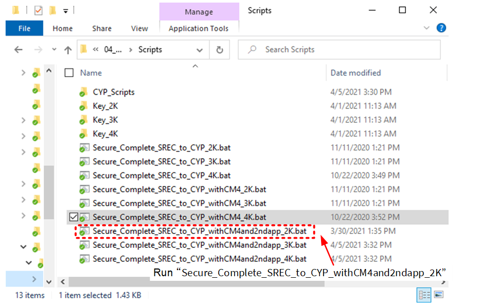
The bat file does the following: Signs the CM0+ first application ELF file and second application ELF file
- Merges the ELF files of first application and second application.
- Generates a cm0plus_si.elf.srec file from the merged ELF file.
- Signs the CM4 ELF file and generate cm4_si.elf.srec from the signed CM4 ELF file.
- Makes sure the SREC files are in the CYP_Scripts
- Connect MiniProg4 to the target board and run enable_sflashandprogram.bat in CYP_Scripts folder.
Appendix J - Dummy application header implementation
If the bootloader enabling conditions are met, the device may transition to DEAD state by erasing the first application software. As a result, the second application software will not be activated even if it is implemented. In this case, second application can be activated by programming a dummy application header instead of the first application software or disabling bootloader. This section describes the implementation of the dummy application header.
Implementation
This project provides a file for the dummy application header implementation, which is available in:\tviibe1m\tools\ghs
Sample project stored folder
Following is the configuration of the sample project:
- Application header address: 0x10000000
- Object size: 0xFE00
- Application ID/version: 0x00010000
- Attribute: 0
- Number of cores(N): 1
- Core(i) VT offset: 0xF0
- Core(i) CPU ID and core index: 0xC6000000
Change these parameters according to your system. The sample programs and scripts shown here use the CYT2B7 series.
- Configure the project:
- Open the project window:
- Copy tviibe1m_common_app_header.gpj and options_global_app_header.opt from the \tviibe1m\tools\ghs\_gpj_app_header folder to the \ tviibe1m\tools\ghs folder.Figure 22. Project configuration for application header 1
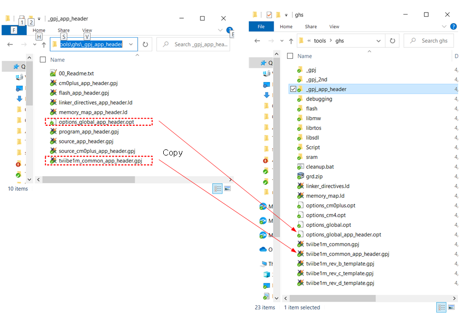
- Right-click tviibe1m_rev_d_template.gpj,
- Select Add File into tviibe1m_common.gpj…
- Add tviibe1m_common_app_header.gpj.Figure 23. Project configuration for application header 2

- Prepare the source file
- Copy the main_cm0plus_app_header.c file from the \ tviibe1m\src\dummy_first_app_hdr folder to the \ tviibe1m\src folder.
- Build and program
- Build a flash_app_header project using GHS Multi.Figure 24. Build project for application header
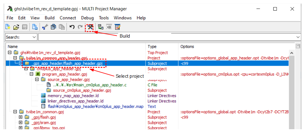
The following is an example of the SREC file of the application header.
S00F0000636D30706C75735F61700000FC S3151000000000FE0000000001000000000001000000DA S30D10000010F0000000000000C61C S50500000002F8 S70500000000FA
- Connect MiniProg4 to the target board and run enable_appheaderprogram.bat in the CYP_Scripts folder. The bat file does the following:
- Copies the cm0plus_app_header.elf.srec file.
- Erases the first application software area (0x10000000 to 0x1000FFFF).
- Programs the cm0plus_app_header.elf.srec.
Appendix K - Compile and linker options
The following options are required when building a secure boot using Green Hills MULTI.
- Compile option: Set the C language dialect to ISO C99.
This setting is required to configure the secure image using the sample project.
- Select the target project.
- Select Edit > Set Build Options....
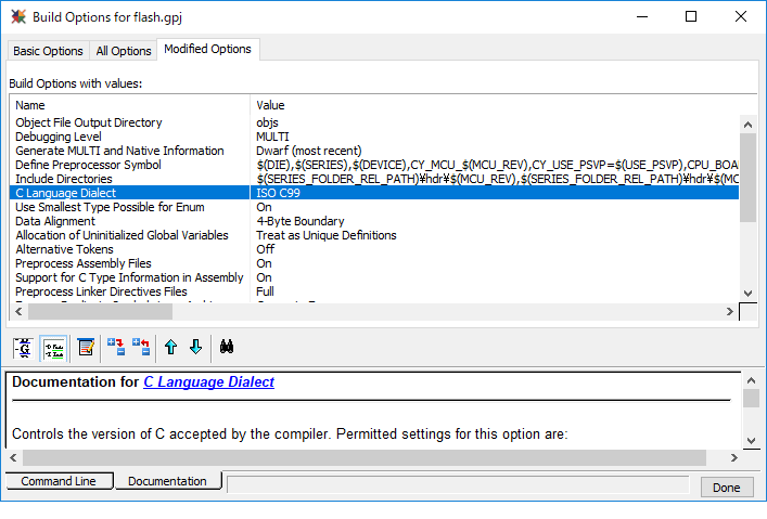
- Linker option: Set the physical address offset from the virtual address to ‘0’.
This setting is required to generate a digital signature using the cymcuelftool.exe tool.
-
Select program.gpj in cm0plus.gpj.
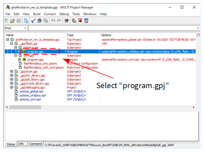
-
Select Edit > Set Build Options...., and then select the All Options tab.
-
In the Option Categories list, expand the Advanced group, and then select Linker Options.
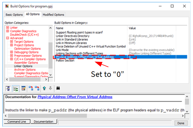
-
Set the same configuration to program.gpj in cm4.gpj.
- Generate the SREC file.
As mentioned earlier, the blank area in the code must be ‘0’ for digital signature authentication. The following shows how to fill the blank area of the SREC file with ‘0’ for GHS MULTI. The SREC file is generated using the gsrec utility.
gsrec.exe input_file (.elf) -o out_file (.srec) -bytes 16 -fill1 0x10000000 0x1000FEFF 0x00
References
The following are the TRAVEO™ T2G family series datasheets and technical reference manuals. Contact Technical Support to obtain these documents, code snippets, sample driver library (SDL), and tools used in this application note. Note that the obtained sample program does not conform to automotive standards, so it is used only as an example for secure system configuration and cannot be used for production purposes.
- Device datasheet
- CYT2B7 datasheet 32-bit Arm® Cortex®-M4F microcontroller TRAVEO™ T2G family
- CYT2B9 datasheet 32-bit Arm® Cortex®-M4F microcontroller TRAVEO™ T2G family
- CYT4BF datasheet 32-bit Arm® Cortex®-M7 microcontroller TRAVEO™ T2G family
- CYT4DN datasheet 32-bit Arm® Cortex®-M7 microcontroller TRAVEO™ T2G family (Doc No. 002-24601)
- CYT3BB/4BB datasheet 32-bit Arm® Cortex®-M7 microcontroller TRAVEO™ T2G family
- CYT3DL datasheet 32-bit Arm® Cortex®-M7 microcontroller TRAVEO™ T2G family (Doc No. 002-27763)
- Technical reference manual
- Body controller entry family
- Body controller high family
- Cluster 2D family
- TRAVEO™ T2G Automotive Cluster 2D family architecture technical reference manual (TRM) (Doc No. 002-25800)
- TRAVEO™ T2G Automotive Cluster 2D registers technical reference manual (TRM) for CYT4DN (Doc No. 002-25923)
- TRAVEO™ T2G Automotive Cluster 2D registers technical reference manual (TRM) for CYT3DL (Doc No. 002-29854)
Revision history
Document version | Date of release | Description of changes |
|---|---|---|
** | 2020-03-24 | New Application Note. |
*A | 2021-05-24 | Added chapter 7.3 Added note for RMA lifecycle transition Added RSA-3072/4096 support Changed Appendix G, H Added Appendix I, J MOVED TO INFINEON TEMPLATE. |
*B | 2021-08-18 | Added description to section 8.1 for Bootloader. Added section 7.3 and 16.3. Changed TOC2 table for Security Marker. Added CYT3BB/4BB, CYT3DL to supported devices. |
*C | 2022-07-04 | Added a note in RMA for Open RMA behavior in the SECURE_WITH_DEBUG lifecycle stage. Added a note in Code validation for boot authentication of application software. Changed sample program folder location and file name. |
*D | 2023-09-06 | Added note in What is a secure system? |
*E | 2023-11-16 | Template update;no content update. |