AN220203 Smart I/O usage setup in TRAVEO™ T2G family
About this document
Scope and purpose
AN220203 describes how to use Smart I/O in TRAVEO™ T2G MCUs. Smart I/O adds a programmable logic circuitry between a peripheral and a GPIO port, thereby integrating board-level glue logic.
Associated part family
TRAVEO™ T2G family CYT2/CYT3/CYT4 series
Introduction
This application note describes how to use and setup Smart I/O in Infineon TRAVEO™ T2G family CYT2/CYT3/CYT4 series MCUs.
Smart I/O adds programmable logic to an I/O port. Smart I/O integrates Boolean logic functionality such as AND, OR, and XOR into a port. It also pre- or post-processes the signals between high-speed I/O matrix (HSIOM) and I/O port. For example, Smart I/O can enable digital glue logic for input signals using multiple flip-flops without CPU intervention. HSIOM multiplexes GPIOs sharing multiple functions into peripheral devices selected by the user. See the Architecture Technical Reference Manual (TRM) for details of HSIOM.
To understand the functionality described and terminology used in this application note, see the Smart I/O chapter in the Architecture TRM. Figure 1 shows examples of typical signal paths.
Figure 1. Smart I/O interface

Path 1: Implements self-contained logic functions that directly operate on I/O port signals
Path 2: Implements self-contained logic functions that operate on HSIOM signals
Path 3: Logic conversed HSIOM output signals route to I/O port
Path 4: Logic conversed I/O port input signals route to HSIOM
For each signal path, the Smart I/O function gives an option for a programmable output. This application note shows the example usage and configuration of the Smart I/O function.
Applications of Smart I/O
Smart I/O can be used whenever simple logic operations and routing are required to be performed on signals to or from the I/O pins. Typical applications include the following:
- Change routing to/from pins: This function allows rerouting signals from the fixed-function peripherals to non-dedicated pins on the same port.
- Invert the polarity of signal: This function inverts the polarity of output signals, such as the SPI signal, before it goes out from a pin.
- Clock or signal buffer: This function drives a GPIO input signal, which has to drive a heavier load for one pin, through two GPIO buffers.
- Detect a pattern on pins: This function detects the patterns of several signal inputs and outputs the programmable signal depending on the result of detection.
These applications of Smart I/O can work in low-power mode (DeepSleep), therefore can be used as a wakeup interrupt.
Bypass of Smart I/O
When the Smart I/O function is not used, it will be automatically bypassed by setting the SMARTIO_PRTx_CTL.ENABLE1 bit to “0”: Disabled. It is also possible to bypass any I/O pin in the Port group using the SMARTIO_PRTx_CTL.BYPASS bits. When BYPASS bits are set to “1”: Bypass, HSIOM and I/O port are connected directly.
Note that the bypass setting must be configured before enabling the Smart I/O. (SMARTIO_PRTx_CTL.ENABLE set to “1”: Enabled)
Table 1 shows the description of the SMARTIO_PRTx_CTL register for bypass setting. See the Registers TRM for details.
Table 1. Register for Bypass setting
Register | Bit Field | Setting |
|---|---|---|
SMARTIO_PRTx_CTL | BYPASS [7:0] | Bypass Smart I/O ‘0’: No bypass (Smart I/O is present in the signal path) ‘1’: Bypass (Smart I/O is absent in the signal path) |
ENABLED [31] | Enable Smart I/O 0: Disabled (Signals are bypassed: default) 1: Enabled (Should only be set to ‘1’ when Smart I/O is completely configured.) |
Structure of Smart I/O
Figure 2 shows the block diagram of Smart I/O. Smart I/O is positioned in the signal path between the HSIOM and the I/O port.
Figure 2. Block Diagram of Smart I/O

The Smart I/O consists of the following components:
- Clock and reset
- Synchronizer (Sync)
- 3-input lookup tables (LUT3 [x]): x = 0 to 7
- Data unit (DU)
Smart I/O is implemented for the specified I/O cell. Smart I/O can provide programmable signals to HSIOM and I/O port with a combination of these components. See the Package Pin List and Alternate Functions of Device Datasheet for details on the I/O port that can be used as Smart I/O.
The io_data_in [7:0] is the input signal from the I/O port, while the chip_data [7:0] is the input signal from HSIOM. These signals are input to Smart I/O via the Sync components (synchronizer). The smartio_data [7:0] is the output signal from Smart I/O. These signals are routed or modified by Smart I/O and output to the I/O port or HSIOM.
The clk_block is used for all components in Smart I/O. The clk_block can be selected from the I/O port input signals (io_data_in [7:0]), HSIOM input signals (chip_data [7:0]), clk_smartio, and clk_lf. The clk_smartio is derived from the system clock (clk_sys/CLK_HF) using a peripheral clock divider, and the clk_smartio is input in the Clock and Reset block. See the Clocking system chapter of Architecture TRM for details on clk_smartio and clk_lf.
Eight lookup tables (LUT3 [x]) are implemented for each Smart I/O unit. LUT3 [x] can provide the programmable output, and it can decide the connection of signals between HSIOM and the I/O port. This means that the eight lookup tables offer a flexible routing combination of input channel and output.
The data unit can provide enhanced functionality for the output signal. Clock and Reset block is used to synchronize the signals of HSIOM, I/O port, and each block in Smart I/O. Synchronizer controls the synchronization/asynchronization of the HSIOM input and the I/O port input.
Clock and Reset
Smart I/O can provide reset signals and clock selection. Figure 3 shows the selection logic of the configuration of clock and reset.
Figure 3. Functional image of clock and reset setting

When io_data_in [7:0] and chip_data [7:0] are selected as the clock source, the clocks have no associated reset. When clk_smartio is selected as the clock source, either rst_sys_act_n or rst_sys_dpslp_n can be used depending on the operating power mode: Active or DeepSleep. When clk_lf is selected as the clock source, rst_lf_dpslp_n can be used. The clock (clk_block) and reset (rst_block_n) can be set by the SMARTIO_PRTx_CTL.CLOCK_SRC [12:8] register.
The following clock sources are available for selection:
- io_data_in [7:0]: These are I/O port input signals.
- chip_data [7:0]: These are HSIOM input signals.
- clk_smartio: This clock is derived from the system clock clk_sys/CLK_HF.
- clk_lf: This clock is a low-frequency system clock. This clock is only available in DeepSleep mode.
The following reset sources are available for selection:
- rst_sys_act_n: Smart I/O is active only in Active power mode with the clock from the peripheral divider.
- rst_sys_dpslp_n: Smart I/O is active in all power modes except in DeepSleep mode with the clock from the peripheral divider.
- rst_lf_dpslp_n: Smart I/O is active in all power modes with the clock from ILO.
Table 2 shows the configuration of the SMARTIO_PRTx_CTL.CLOCK_SRC [12:8] register. See the Registers TRM for details.
Table 2. Register for Clock and Reset setting
Register | Bit Field | Setting |
|---|---|---|
SMARTIO_PRTx_CTL | CLOCK_SRC [12:8] | Clock (clk_block)/Reset (rst_block_n) source selection:
|
Synchronizer
Each input signal at the I/O port and HSIOM can be used either in synchronous or asynchronous mode. The synchronizer synchronizes the input signal with the Smart I/O clock (clk_block).
Table 3 shows synchronizer setting register and configuration. See the Registers TRM for details.
Table 3. Register for Synchronizer Setting
Register | Bit Field | Setting |
|---|---|---|
SMARTIO_PRTx_SYNC_CTL | IO_SYNC_EN [7:0] | Synchronization of the io_data_in [7:0] signals with clk_block 0: No synchronization 1: Synchronization |
CHIP_SYNC_EN [15:8] | Synchronization of the chip_data [7:0] signals with clk_block 0: No synchronization 1: Synchronization |
3-inputs lookup tables (LUT3 [x])
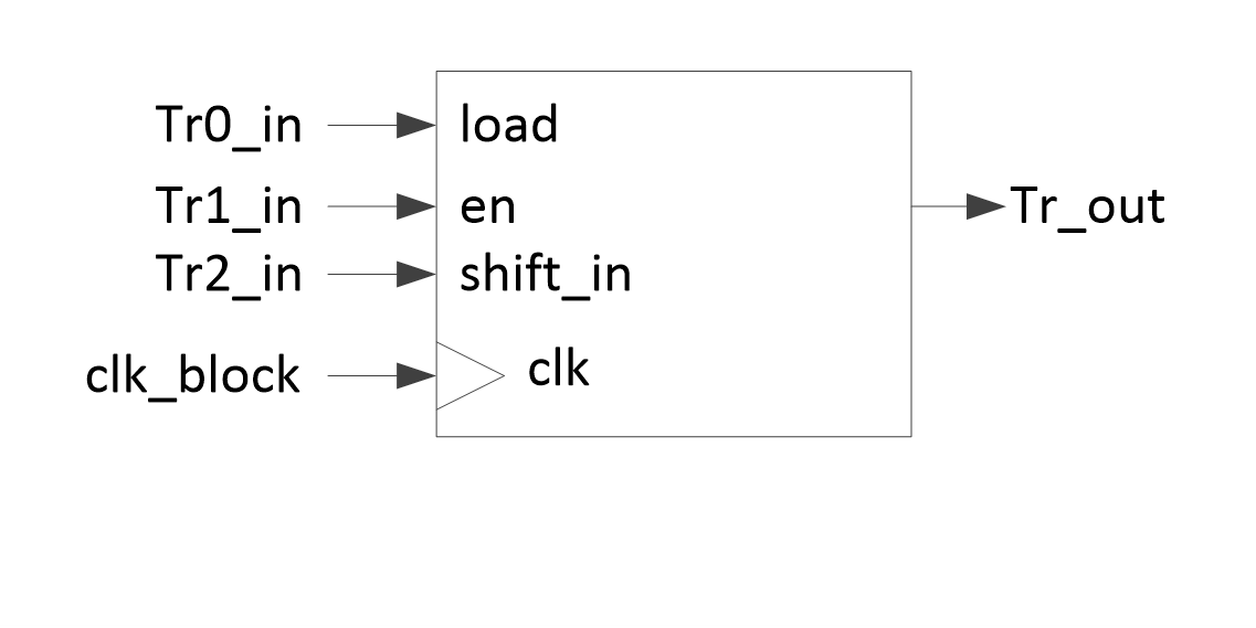
Each LUT3 [x] has three inputs and one output. All inputs (Tr0_in, Tr1_in, Tr2_in) of each LUT3 [x] block should be selected. If there is only one input operation, provide the input to all three input sources (Tr0_in, Tr1_in, Tr2_in). Each LUT3 [x] takes three input signals and generates an output based on the configuration set in register. Figure 4 shows the basic block diagram of each LUT3 [x]. The output pattern can be set by the register.
Figure 4. LUT3 [x] Block Diagram

LUT3 [x] output configuration
Output signal (Tr_out) of LUT3 [x] can be programmed using SMARTIO_PRTx_LUT_CTLy.LUT[7:0]2 based on three input sources (Tr2_in, Tr1_in, Tr0_in). Table 4 shows example of setting each LUT3 [x].
Table 4. LUT3 [x] output setting
Tr 2_in | Tr 1_in | Tr 0_in | Tr_out | Tr_out(Example 1) | Tr_out(Example 2) |
|---|---|---|---|---|---|
0 | 0 | 0 | A | 0 | 0 |
0 | 0 | 1 | B | 0 | 0 |
0 | 1 | 0 | C | 0 | 1 |
0 | 1 | 1 | D | 0 | 0 |
1 | 0 | 0 | E | 1 | 1 |
1 | 0 | 1 | F | 1 | 0 |
1 | 1 | 0 | G | 1 | 0 |
1 | 1 | 1 | H | 1 | 0 |
Eight output patterns (A to H) are generated for three input signals. Each output from A to H is a Boolean value of 0 or 1. This output pattern value [H, G, F, E, D, C, B, A] is set in the LUT [7:0].
In case of example 1, the output pattern is [H, G, F, E, D, C, B, A] = [1, 1, 1, 1, 0, 0, 0, 0]. Therefore, the value "0xF0" is set to LUT [7:0]. Also, in the case of example 2, the output pattern is [H, G, F, E, D, C, B, A] = [0, 0, 0, 1, 0, 1, 0, 0]. Therefore, the set value is "0x14" to LUT [7:0].
Table 5 shows the SMARTIO_PRTx_LUT_CTLy.LUT [7:0] register for LUT3 [x] output setting. See the Registers TRM for details.
Table 5. Register for Setting the Output from LUT3 [x]
Register | Bit Field | Setting |
|---|---|---|
SMARTIO_PRTx_LUT_CTLy | LUT [7:0] | LUT3 [x] configuration. Depending on the LUT opcode (LUT_OPC), internal state and LUT3 [x] input signals tr0_in, tr1_in, and tr2_in, the LUT3 [x] configuration is used to determine the LUT3[x] output signal and the next sequential state. |
LUT3 [x] input selection
The input sources (Tr0_in, Tr1_in, Tr2_in) of each LUT3 [x] can be selected from the following:
- Data unit output
- Other LUT3 [x] output signal (Tr_out)
- Input signal from HSIOM (chip_data [7:0])
- Input signal from I/O port (io_data_in [7:0])
LUT3[7] to LUT3[4] operate on io_data/chip_data[7] to io_data/chip_data[4], whereas LUT3[3] to LUT3[0] operate on io_data/chip_data[3] to io_data/chip_data[0].
The input sources can be configured with LUT_TR0_SEL [3:0], LUT_TR1_SEL [11:8], and LUT_TR2_SEL [19:16] in the SMARTIO_PRTx_LUT_SELy register. Table 6 shows the SMARTIO_PRTx_LUT_SELy register and input selection setting. Note that Data Unit output can only be input to tr0_in. See the Registers TRM for details.
Table 6. Register for LUT3 [x] Input Source Setting
Register | Bit Field | Setting |
|---|---|---|
SMARTIO_PRTx_LUT_SELy | LUT_TR0_SEL [3:0] | LUT3 [x] input signal tr0_in source selection: 0: Data unit output 1: LUT3 [1] output 2: LUT3 [2] output 3: LUT3 [3] output 4: LUT3 [4] output 5: LUT3 [5] output 6: LUT3 [6] output 7: LUT3 [7] output 8: chip_data [0] (for LUT3 [0], [1], [2], [3]); chip_data [4] (for LUT3 [4], [5], [6], [7]) 9: chip_data [1] (for LUT3 [0], [1], [2], [3]); chip_data [5] (for LUT3 [4], [5], [6], [7]) 10: chip_data [2] (for LUT3 [0], [1], [2], [3]); chip_data [6] (for LUT3 [4], [5], [6], [7]) 11: chip_data [3] (for LUT3 [0], [1], [2], [3]); chip_data [7] (for LUT3 [4], [5], [6], [7]) 12: io_data_in [0] (for LUT3 [0], [1], [2], [3]); io_data_in [4] (for LUT3 [4], [5], [6], [7]) 13: io_data_in [1] (for LUT3 [0], [1], [2], [3]); io_data_in [5] (for LUT3 [4], [5], [6], [7]) 14: io_data_in [2] (for LUT3 [0], [1], [2], [3]); io_data_in [6] (for LUT3 [4], [5], [6], [7]) 15: io_data_in [3] (for LUT3 [0], [1], [2], [3]); io_data_in [7] (for LUT3 [4], [5], [6], [7]) |
LUT_TR1_SEL [11:8] / LUT_TR2_SEL [19:16] | LUT3 [x] input signal tr1_in / tr2_in source selection: 0: LUT3 [0] output 1: LUT3 [1] output 2: LUT3 [2] output 3: LUT3 [3] output 4: LUT3 [4] output 5: LUT3 [5] output 6: LUT3 [6] output 7: LUT3 [7] output 8: chip_data [0] (for LUT3 [0], [1], [2], [3]); chip_data [4] (for LUT3 [4], [5], [6], [7]) 9: chip_data [1] (for LUT3 [0], [1], [2], [3]); chip_data [5] (for LUT3 [4], [5], [6], [7]) 10: chip_data [2] (for LUT3 [0], [1], [2], [3]); chip_data [6] (for LUT3 [4], [5], [6], [7]) 11: chip_data [3] (for LUT3 [0], [1], [2], [3]); chip_data [7] (for LUT3 [4], [5], [6], [7]) 12: io_data_in [0] (for LUT3 [0], [1], [2], [3]); io_data_in [4] (for LUT3 [4], [5], [6], [7]) 13: io_data_in [1] (for LUT3 [0], [1], [2], [3]); io_data_in [5] (for LUT3 [4], [5], [6], [7]) 14: io_data_in [2] (for LUT3 [0], [1], [2], [3]); io_data_in [6] (for LUT3 [4], [5], [6], [7]) 15: io_data_in [3] (for LUT3 [0], [1], [2], [3]); io_data_in [7] (for LUT3 [4], [5], [6], [7]) |
Each LUT3 [x] has limited connections with input/output of HSIOM and I/O port signals. Sometimes, multiple LUT3 [x] are necessary for a complete flexible routing.
The LUT3 [x] and data unit do not include any combinatorial loops. However, when one LUT3 [x] interacts with the other or to the data unit, inadvertent combinatorial loops are possible. To overcome this limitation, the SMARTIO_PRTx_CTL.PIPELINE_EN bit is used. When set, all outputs (LUT3 [x] and data unit) are registered before branching out to other components. Table 7 shows PIPELINE_EN setting. This bit is set to “1” (Enabled) to ensure low power consumption, if Smart I/O is not used. See the Registers TRM for details.
Table 7. PIPELINE_EN Setting
Register | Bit Field | Setting |
|---|---|---|
SMARTIO_PRTx_CTL | PIPELINE_EN [25] | Enable for pipeline register: 0: Disabled (Register is bypassed) 1: Enabled (Default value) |
LUT3 [x] operation
Each LUT3 [x] has the following four operations selected by a 2-bit Op Code field. The four operations are:
Combinatorial
LUT3 [x] is purely combinatorial. Each LUT3 [x] output is the result of the LUT mapping truth table, and will only be delayed by the LUT3 [x] combinatorial path (Basic mode).
Figure 5. Combinatorial

Gated Input 2
LUT3 [x] input 2 is registered. Other inputs are directly connected to LUT3 [x]. The output is combinatorial (Input synchronization).
Figure 6. Gated Input2

Gated Output
Inputs are directly connected to LUT3 [x] and the output is registered (Output synchronization).
Figure 7. Gated output

Set/reset flip-flop
Input signals are used to control an S/R flip-flop.
Figure 8. S/R flip-flop enable

These four operations can be set with the register shown in Table 8. See the for details.
Table 8. Register for LUT3 [x] Mode Setting
Register | Bit Field | Setting |
|---|---|---|
SMARTIO_PRTx_LUT_CTLy | LUT_OPC [9:8] | 0: Combinatorial 1: Gated Input 2 2: Gated Output 3: Set/reset flip-flop |
Data Unit (DU)
Each Smart I/O block includes a data unit (DU) component. DU consists of a simple 8-bit data path. It is capable of performing simple increment, decrement, increment/decrement, shift, and AND/OR operations. DU can generate a programmable output (Tr_out) signal based on two 8-bit data inputs that DATA0 (data0_in [7:0]) and DATA1 (data1_in [7:0]). The internal state is captured in flip-flops. The DU behavior can be controlled by up to three input signals (Tr0_in, Tr1_in, Tr2_in). Figure 9 shows the basic block diagram of Data Unit.
Figure 9. Data Unit Block Diagram

Input selection
DU has up to three control input signals. These signals can be selected as input from the following.
- Constant “0”
- Constant “1”
- DU output
- LUT3 [x] outputs
The number of control signals required depends on the DU operation code.
These inputs can be configured with the SMARTIO_PRTx_DU_SEL register. Table 9 shows the SMARTIO_PRTx_DU_SEL register and input selection setting. See the Registers TRM for details.
Table 9. Register for DU Inputs Source Setting
Register | Bit Field | Setting |
|---|---|---|
SMARTIO_PRTx_DU_SEL | DU_TR0_SEL [3:0] / DU_TR1_SEL [11:8] / DU_TR2_SEL [19:16] | Data unit input signal “tr0_in” / “tr1_in” / “tr2_in” source selection: 0: Constant ‘0’ 1: Constant ‘1’ 2: Data unit output 3- 10: LUT3 [x] outputs Otherwise: Undefined |
DATA 0 and DATA 1 use input data for DU logic to be initialized. These data can be selected from the following:
- Constant 0x00
- io_data_in [7:0]
- chip_data_in [7:0]
- DATA [7:0] bits of SMARTIO_PRTx_DATA register
The data width handled by the data unit can be changed between 1 bit and 8 bits. Table 10 shows the configuration registers for input data to DU.
Table 10. Register for DU Data Setting
Register | Bit Field | Setting |
|---|---|---|
SMARTIO_PRTx_DU_SEL | DU_DATA0_SEL [25:24] / DU_DATA1_SEL [29:28] | Data unit input data “data0_in” / “data1_in” source selection: 0: 0x00 1: chip_data [7:0]. 2: io_data_in [7:0]. 3: SMARTIO_PRTx_DATA.DATA [7:0] MMIO register field. |
SMARTIO_PRTx_DATA | DATA [7:0] | Data unit input data source |
SMARTIO_PRTx_DU_CTL | DU_SIZE [2:0] | Size/width of the data unit (in bits) is DU_SIZE+1. |
Operation of data unit
The DU operation is defined by SMARTIO_PRTx_DU_CTL.DU_OPC [11:8]. Table 11 shows the configuration registers for DU operation code setting. See the Registers TRM for details.
Table 11. DU Operation Code Configuration
Register | Bit Field | Setting |
|---|---|---|
SMARTIO_PRTx_DU_CTL | DU_OPC [11:8] | Data unit opcode specifies the data unit operation: "1": INCR "2": DECR "3": INCR_WRAP "4": DECR_WRAP "5": INCR_DECR "6": INCR_DECR_WRAP "7": ROR "8": SHR "9": AND_OR "10": SHR_MAJ3 "11": SHR_EQL Otherwise: Undefined Default Value: Undefined |
Table 12 shows each DU operation.
The ‘Operation’ column in Table 12 shows the operation outline and the pseudo code. In the pseudo code, “Combinational:” indicates that the operations are independent of previous output states. "Registered:" indicates that data operates on inputs and previous output states (registered using flip-flops).
Table 12. DU Operation
Operation code | Operation |
|---|---|
DU_OPC [11:8] = 1: INCR | INCR increments data by 1 from an initial value (DATA 0) until it reaches a final value (DATA 1). Combinational: |
DU_OPC [11:8] = 2: DECR | DECR decrements data from an initial value (DATA 0) until it reaches ‘0’. Combinational: Registered: |
DU_OPC [11:8] = 3: INCR_WRAP | INCR_WRAP operates similar to INCR, but instead of stopping at DATA 1, it wraps around to DATA 0. Combinational: Registered: |
DU_OPC [11:8] = 4: DECR_WRAP | DECR_WRAP works similar to DECR. Instead of stopping at ‘0’, it wraps around to DATA0. Combinational: Registered: |
DU_OPC [11:8] = 5: INCR_DECR | INCR_DECR is a combination of INCR and DECR. Depending on the trigger signals, it either starts incrementing or decrementing. Increment stops at DATA 1 and decrement stops at ‘0’. Combinational: Registered: |
DU_OPC [11:8] = 6: INCR_DECR_WRAP | INCR_DECR_WRAP has the same functionality as INCR_DECR with wrap around to DATA 0 on reaching the limits (DATA 1 or ‘0’). Combinational: Registered: |
DU_OPC [11:8] = 7: ROR | POR rotates the data right and the LSB is sent out. The data for rotation is taken from DATA 0. Combinational: Registered: |
DU_OPC [11:8] = 8: SHIR | SHIR performs the shift register operation. Initial data (DATA 0) is shifted out and data on tr2_in is shifted in. Combinational: Registered |
DU_OPC [11:8] = 9: AND_OR | ANDs data1 and data0 along with mask; then, ORs all bits of the ANDed output Combinational: Registered: |
DU_OPC [11:8] = 10: SHR_MAJ3 (Majority 3) | SHR_MAJ3 performs the same functionality as SHR. Instead of sending the shifted-out value, it sends a ‘1’, if at least two samples are high in the last three samples/shifted-out values of data [0]. Otherwise, it sends a ‘0’. This function sends out the majority of the last three samples. Combinational: Registered: |
DU_OPC [11:8] = 11: SHR_EQL (Match DATA1) | SHR_EQL performs the same operation as SHR. Instead of shift-out, the output is the comparison result (DATA 0 == DATA 1). Combinational:
Registered: |
Smart I/O configuration
Figure 10 shows an example of the configuration flow of Smart I/O.
Figure 10. Smart I/O Configuration Flow

When configuring Smart I/O, first initialize each component such as clock and reset, synchronizer, LUT3 [x] and DU. Before enabling Smart I/O (SMARTIO_PRTx_CTL.ENABLE set to “1”: Enabled), all components and routing should be configured.
If Smart I/O is not used, clock selection in clock and reset component should be set to a value between 20 to 30, and PIPELINE_EN should be set to “1”, to ensure low power consumption.
Note:
(*1) See Structure of Smart I/O for ports, source and clock setting, see 3-inputs lookup tables (LUT3 [x]) for LUT3 [x] setting, and see Data Unit (DU) for DU setting.
(*2) See Table 3 for Synchronization setting.
(*3) See Table 1 for bypass and Smart I/O enable setting.
(*4) See Table 7 for PIPELINE_EN setting.
Example configuration
This section describes how to use Smart I/O using the Sample Driver Library (SDL). The code snippets in this application note are part of SDL. See Other references for the SDL.
SDL basically has a configuration part and a driver part. The configuration part mainly configures the parameter values for the desired operation. The driver part configures each register based on the parameter values in the configuration part. You can configure the configuration part according to your system.
Smart I/O can be useful for an application that involves simple logic operations for input/output signal, or the internal routing between internal HSIOM port and the I/O port. No CPU is required for these operations. This section explains how to use Smart I/O according to the use case.
In this example, CYT2B7 series is used.
Use case to change routing from I/O pins to HSIOM by inverting polarity
This section explains an example of routing and simple logic operations by using Smart I/O.
In this use case, routing is changed to connect the input from pin 7 of Port 13 (io_data_in [7]) to pin 1 of HSIOM (smartio_data [1]). In addition, the polarity of io_data_in [7] is inverted, and the inverted io_data_in [7] signal is output to smartio_data [1]. See the Package Pin List and Alternate Functions of Device Datasheet for I/O port which can used Smart I/O.
Figure 11 shows the connection from the I/O port to HSIOM with signal inverting. LUT3 [1] and LUT3 [7] are used for this use case.
Figure 11. Signal Inverting Image

Figure 12 shows the signal path of this example.
Figure 12. Example of the Overview of Routing

Note that LUT3 [1] and LUT3 [7] are used. LUT3[7:4] that can use io_data [7] as input cannot be routed to smartio_data [1] directly. Therefore, output of LUT3 [7] must go through LTU3 [1] which can be routed to smartio_data [1]. In this use case, LUT3 [1] inverts the input signal from LUT3 [7] and outputs it to smartio_data [1].
Table 13 shows the truth table of LUT3 [7] and Table 14 shows the truth table of LUT3 [1]. The bold highlights in the tables indicate an invalid combination pattern.
Table 13. Look Up Table LUT3 [7]
Tr2_in | Tr1_in | Tr0_in | Tr_out |
|---|---|---|---|
0 | 0 | 0 | 0 |
0 | 0 | 1 | 0 |
0 | 1 | 0 | 0 |
0 | 1 | 1 | 0 |
1 | 0 | 0 | 0 |
1 | 0 | 1 | 0 |
1 | 1 | 0 | 0 |
1 | 1 | 1 | 1 |
Table 14. Look Up Table LUT3 [1]
Tr2_in | Tt1_in | Tr0_in | Tr_out |
|---|---|---|---|
0 | 0 | 0 | 1 |
0 | 0 | 1 | 1 |
0 | 1 | 0 | 1 |
0 | 1 | 1 | 1 |
1 | 0 | 0 | 1 |
1 | 0 | 1 | 1 |
1 | 1 | 0 | 1 |
1 | 1 | 1 | 0 |
The three inputs of LUT3 [1] are input same signal, Similarly, LUT3 [7] are input same signal. Therefore, the input pattern of LTU3s is [Tr2_in, Tr1_in, Tr0_in] = [0, 0, 0] or [1, 1, 1].
LUT3 [7] does not change polarity. That is, Tr_out is “1”, when [Tr2_in, Tr1_in, Tr0_in] = [1, 1, 1], and otherwise, Tr_out = “0”.
LUT3 [1] reverses polarity. That is, Tr_out is “0”, when [Tr2_in, Tr1_in, Tr0_in] = [1, 1, 1], and otherwise, Tr_out = “1”.
Figure 13 shows the setting procedure for Smart I/O.
Figure 13. Setting procedure for Smart I/O

(a) See the Table 14 for setting pattern.
(b) See the Table 13 for setting pattern.
Configuration and example code
Table 15 lists the parameters and Table 16 lists the functions of the configuration part in SDL for Smart I/O.
Table 15. List of Smart I/O configuration Parameters
Parameters | Description | Value |
|---|---|---|
SMART_IO_CLK_ACTIVE | Defines Smart I/O clock source | 1ul (Select Active clock source) |
CY_SMARTIO_CLK_INV | Defines Smart I/O clock | PCLK_SMARTIO13_CLOCK |
SMART_IO_PORT | Defines Smart IO port | SMARTIO_PRT13 (It is assigned to Smar I/O Port13) |
SMARTIO_BYPASS_CH_MASK | Defines Bypass channel mask io_data_in [7] to smartio_data [7]: No bypass io_data_in [6] to smartio_data [6]: Bypass io_data_in [5] to smartio_data [5]: Bypass io_data_in [4] to smartio_data [4]: Bypass io_data_in [3] to smartio_data [3]: Bypass io_data_in [2] to smartio_data [2]: Bypass io_data_in [1] to smartio_data [1]: No bypass io_data_in [0] to smartio_data [0]: Bypass | 0x7Dul (See Table 1) No use Smart IO for io_data_in [6] to io_data_in [2] and io_data_in [0] |
SMARTIO_IOSYNC_CH_MASK | Defines IO sync channel mask | 0x00ul (See Table 3) |
LUT_IP_BUTTON_PORT | Defines input port for LUT3[7] input | CY_BUTTON2_PORT (It is assigned to GPIO Port 13) |
LUT_IP_BUTTON_PIN | Defines input port pin for LUT3[7] input | CY_BUTTON2_PIN (It is assigned to GPIO Port 7 pin) |
LUT_IP_BUTTON_PIN_MUX | Configures input port pin function | CY_BUTTON2_PIN_MUX (It is assigned to GPIO) |
CY_SMARTIO_LUTTR_IO | Selects LUT3[7] input | CY_SMARTIO_LUTTR_IO7 |
LUT_INV_OUT_PORT | Defines output port for LUT3[7] input | P13_1_PORT (It is assigned to GPIO Port 13) |
LUT_INV_OUT_PIN | Defines output port pin for LUT3[7] input | P13_1_PIN (It is assigned to GPIO Port 1 pin) |
LUT_INV_OUT_PIN_MUX | Configures output port pin function | P13_1_GPIO (It is assigned to GPIO) |
LUTx_OUT_MAP | LUT3[7] output pattern | 0x80ul (See Table 13.) |
LUTx_INV_OUT_MAP | LUT3[1] output pattern | 0x7Ful (See Table 14.) |
LUTx_LOGIC_OPCODE | Select LUT3 Operation Mode | CY_SMARTIO_LUTOPC_COMB (It is assigned to Combinatorial) |
CY_SYSCLK_DIV_16_BIT | Selects Divider Type to 16-bit divider | 1ul |
CY_SMARTIO_ENABLE | Sets to Smart I/O and Pipeline enable | 1ul |
CY_SMARTIO_DISABLE | Sets to Smart I/O and Pipeline Disable | 0ul |
CY_SMARTIO_DEINIT | Resets the Smart I/O to default value | 0ul |
CY_SMARTIO_CHANNEL_ALL | Sets to all pin Smart I/O bypass | 0xfful |
CY_SMARTIO_CLK_DIVACT | Selects the source clock to clk_smartio/rst_sys_act_n. See Table 2. | 16ul |
CY_SMARTIO_CLK_GATED | Selects the source clock to Clock source is a constant ‘0’. See Table 2. | 20ul |
CY_SMARTIO_CLK_ASYNC | Selects the source clock to asynchronous mode/“1”. See Table 2. | 31ul |
CY_SMARTIO_LUTTR_LUT7_OUT | Selects LUT3[1] input | 7ul (It is assigned to LUT3[7] output. See Table 6.) |
CY_SMARTIO_LUTTR_IO7 | Selects LUT3[7] input | 15ul (It is assigned to io_data_in [7] output. See Table 6.) |
smart_io_cfg.clkSrc | Source clock setting | CY_SMARTIO_CLK_DIVACT |
smart_io_cfg.bypassMask | Configures bypass setting | SMARTIO_BYPASS_CH_MASK |
smart_io_cfg.ioSyncEn | Configures Synchronizer setting | SMARTIO_IOSYNC_CH_MASK |
lutCfgLut1.opcode | Configures LUT3[1] Operation Mode setting | LUTx_LOGIC_OPCODE |
lutCfgLut1.lutMap | Configures LUT3[1] output pattern setting | LUTx_INV_OUT_MAP |
lutCfgLut1.tr0 | Configures LUT3[1] tr0 input | CY_SMARTIO_LUTTR_LUT7_OUT |
lutCfgLut1.tr1 | Configures LUT3[1] tr1 input | CY_SMARTIO_LUTTR_LUT7_OUT |
lutCfgLut1.tr2 | Configures LUT3[1] tr2 input | CY_SMARTIO_LUTTR_LUT7_OUT |
lutCfgLut7.opcode | Configures LUT3[7] Operation Mode setting | LUTx_LOGIC_OPCODE |
lutCfgLut7.lutMap | Configures LUT3[7] output pattern setting | CY_SMARTIO_LUTTR_IO |
lutCfgLut7.tr0 | Configures LUT3[7] tr0 input | CY_SMARTIO_LUTTR_IO |
lutCfgLut7.tr1 | Configures LUT3[7] tr1 input | CY_SMARTIO_LUTTR_IO |
lutCfgLut7.tr2 | Configures LUT3[7] tr2 input | CY_SMARTIO_LUTTR_IO |
Table 16. List of Smart I/O Configuration Functions
Functions | Description | Remarks |
|---|---|---|
Init_IO_Pin() | Configures GPIO Port pin | – |
Cy_SmartIO_Deinit() | Resets the Smart I/O to default values | Resets the Smart I/O registers; SMARTIO_PRTx_CTL, SMARTIO_PRTx_SYNC_CTL, SMARTIO_PRTx_LUT_SELy, SMARTIO_PRTx_LUT_CTLy, SMARTIO_PRTx_DU_SEL, SMARTIO_PRTx_DU_CTL and SMARTIO_PRTx_DATA |
Init_SmartIO() | Configures and enables Smart I/O, Call for Init_SmartIO_Cfg() and Cy_SmartIO_Enable() | – |
Init_SmartIO_Cfg() | Configures Smart I/O setting structure, Calls for Cy_SmartIO_Init() | – |
Cy_SmartIO_Enable() | Enable Smart I/O | Write to PIPELINE_EN and ENABLED bit |
Cy_SmartIO_Init() | Configure Smart I/O register | Write to the related registers for Source clock, Bypass, Synchronizer, LUT3, and DU. |
Code Listing 1 demonstrates an example program to change routing from I/O Pins to HSIOM by Inverting Polarity. See the Architecture TRM and Application Note for GPIO and clock configuration.
The following description will help you understand the register notation of the driver part of SDL:
- base signifies the pointer to the Smart I/O register base address.
- base- >unLUT_SEL[idx].u32Register is the SMARTIO_PRTx_LUT_SEL[idx] register mentioned in the Registers TRM. Other registers are also described in the same manner. “ x ” signifies the port suffix number and “ idx ” signifies the register index number.
- To improve the register setting performance, the SDL writes a complete 32-bit data to the register. Each bit field is generated and written to the register as the final 32-bit data.
    un_SMARTIO_PRT_CTL_t workCTL= {.u32Register = 0ul};
    workCTL.stcField.u1ENABLED     = CY_SMARTIO_DISABLE;
    workCTL.stcField.u1PIPELINE_EN = CY_SMARTIO_ENABLE;
    workCTL.stcField.u5CLOCK_SRC   = CY_SMARTIO_CLK_GATED;
    workCTL.stcField.u8BYPASS      = CY_SMARTIO_CHANNEL_ALL;
    base->unCTL.u32Register        = workCTL.u32Register;
See cyip_smartio_v2.h under hdr/rev_x/ip for more information on the union and
structure representation of registers.

##### Code Listing 1 Example to Change Routing from I/O Pins to HSIOM by
Inverting Polarity
``` c


    /* Smart IO clock source selection */
    #define SMART_IO_CLK_ACTIVE             1ul    /* Define Clock active */

    /* Smart IO port selections macro */
    #define SMART_IO_PORT                   SMARTIO_PRT13  /* Define Smart I/O port */

    #define CY_SMARTIO_CLK_INV              PCLK_SMARTIO13_CLOCK  /* Define Smart I/O port */

    /* Bypass channel mask */
    #define SMARTIO_BYPASS_CH_MASK          0x7Dul    /* Define Smart I/O bypass channel */

    /* IO sync channel mask */
    #define SMARTIO_IOSYNC_CH_MASK          0x00ul   /* Define Smart I/O sync channel mask */

    /* Lut input button pin configuration */
    /* Define input port to LUT3[7] */
    #define LUT_IP_BUTTON_PORT              CY_BUTTON2_PORT     /* GPIO_PRT3 */
    #define LUT_IP_BUTTON_PIN               CY_BUTTON2_PIN      /* 7 */
    #define LUT_IP_BUTTON_PIN_MUX           CY_BUTTON2_PIN_MUX  /* P13_7_GPIO */

    #define CY_SMARTIO_LUTTR_IO             CY_SMARTIO_LUTTR_IO7  /**< I/O signal 7 (for LUT 4,5,6,7) */

    /* LUT output pin configuration */
    /* Define output port from LUT3[1] */
    #define LUT_INV_OUT_PORT                P13_1_PORT
    #define LUT_INV_OUT_PIN                 P13_1_PIN
    #define LUT_INV_OUT_PIN_MUX             P13_1_GPIO

    /* LUT output map */
    /* Define LUT3[1] and LUT3[7] output pattern */
    #define LUTx_OUT_MAP                    0x80ul
    #define LUTx_INV_OUT_MAP                0x7Ful

    /* LUT logic circuit type macro */
    #define LUTx_LOGIC_OPCODE               CY_SMARTIO_LUTOPC_COMB  /* Define LUT logic circuit type */

    #define CY_SMARTIO_ENABLE  1ul
    #define CY_SMARTIO_DISABLE 0ul
    #define CY_SMARTIO_DEINIT  0ul
    #define CY_SMARTIO_CHANNEL_ALL  0xfful   /**< All channels */


    /* Button input configuration */
    /* Configure Port for input (Port13 pin) */
    cy_stc_gpio_pin_config_t button_cfg =
    {
        .outVal    = 0ul,
        .driveMode = CY_GPIO_DM_HIGHZ,
        .hsiom     = LUT_IP_BUTTON_PIN_MUX,
        .intEdge   = 0ul,
        .intMask   = 0ul,
        .vtrip     = 0ul,
        .slewRate  = 0ul,
        .driveSel  = 0ul,
    };

    /* Configure Port for output (Port13 pin) */
    cy_stc_gpio_pin_config_t inv_out_cfg =
    {
        .outVal    = 0ul,
        .driveMode = CY_GPIO_DM_STRONG_IN_OFF,
        .hsiom     = LUT_INV_OUT_PIN_MUX,
        .intEdge   = 0ul,
        .intMask   = 0ul,
        .vtrip     = 0ul,
        .slewRate  = 0ul,
        .driveSel  = 0ul,
    };


    int main(void)
    {
        :
        Init_IO_Pin();  /* (1) Configure GPIO pin. See Code Listing 2. */

        /* Deinit before Init */
        Cy_SmartIO_Deinit(SMART_IO_PORT);   /* Disable all Smart I/O. See Code Listing 3 */

        /* SmartIO peripheral clock divider setting */
        {
            /* (3) Configure peripheral Clock */
            Cy_SysClk_PeriphAssignDivider(CY_SMARTIO_CLK_INV, CY_SYSCLK_DIV_16_BIT, 0ul);
            uint32_t sourceFreq = 80000000ul;
            uint32_t targetFreq = 12000000ul;
            uint32_t divNum = (sourceFreq / targetFreq);

            Cy_SysClk_PeriphSetDivider(CY_SYSCLK_DIV_16_BIT, 0ul, (divNum - 1ul));
            Cy_SysClk_PeriphEnableDivider(CY_SYSCLK_DIV_16_BIT, 0ul);
        }

        /* Initialization call for the Smart IO */
        Init_SmartIO();   /* Initialize Smart I/O. See Code Listing 4 */

        for(;;);
    }
Code Listing 2 Init_IO_Pin() Function
    void Init_IO_Pin(void)
    {
        /* Configure Port13 7pin. */
        Cy_GPIO_Pin_Init(LUT_IP_BUTTON_PORT, LUT_IP_BUTTON_PIN, &button_cfg);

        /* Configure Port13 1pin. */
        Cy_GPIO_Pin_Init(LUT_INV_OUT_PORT, LUT_INV_OUT_PIN, &inv_out_cfg);
    }
Code Listing 3 Cy_SmartIO_Deinit() Function
   void Cy_SmartIO_Deinit(volatile stc_SMARTIO_PRT_t* base)
   {
       un_SMARTIO_PRT_CTL_t workCTL= {.u32Register = 0ul};
       /* (2) Disable all Smart I/O port */
       workCTL.stcField.u1ENABLED     = CY_SMARTIO_DISABLE;
       workCTL.stcField.u1PIPELINE_EN = CY_SMARTIO_ENABLE;
       workCTL.stcField.u5CLOCK_SRC   = CY_SMARTIO_CLK_GATED;
       workCTL.stcField.u8BYPASS      = CY_SMARTIO_CHANNEL_ALL;
       base->unCTL.u32Register        = workCTL.u32Register;

       base->unSYNC_CTL.u32Register = CY_SMARTIO_DEINIT;
       for(uint8_t idx = CY_SMARTIO_LUTMIN; idx < CY_SMARTIO_LUTMAX; idx++)
       {
           base->unLUT_SEL[idx].u32Register = CY_SMARTIO_DEINIT;
           base->unLUT_CTL[idx].u32Register = CY_SMARTIO_DEINIT;
       }
       base->unDU_SEL.u32Register = CY_SMARTIO_DEINIT;
       base->unDU_CTL.u32Register = CY_SMARTIO_DEINIT;
       base->unDATA.u32Register = CY_SMARTIO_DEINIT;
   }
Code Listing 4 Init_SmartIO() Function
    void Init_SmartIO(void)
    {
        cy_en_smartio_status_t retStatus = (cy_en_smartio_status_t)0xFF;

        retStatus = Init_SmartIO_Cfg();  /* Configure Smart I/O. See Code Listing 5 */
        if(retStatus == CY_SMARTIO_SUCCESS)
        {
            /* After all the configuration, enable SMART IO */
            Cy_SmartIO_Enable(SMART_IO_PORT);   /* Enable Smart I/O. See Code Listing 6 */
        }
    }
Code Listing 5 Init_SmartIO_Cfg() Function
    cy_en_smartio_status_t Init_SmartIO_Cfg(void)
    {
        cy_stc_smartio_lutcfg_t lutCfgLut1;
        cy_stc_smartio_lutcfg_t lutCfgLut7;

        cy_stc_smartio_config_t smart_io_cfg;
        cy_en_smartio_status_t retStatus = (cy_en_smartio_status_t)0xFF;

        /* initialize the Smart IO structure */
        memset(&lutCfgLut1, 0, sizeof(cy_stc_smartio_lutcfg_t));
        memset(&lutCfgLut7, 0, sizeof(cy_stc_smartio_lutcfg_t));
        /* Clear configuration structure */
        memset(&smart_io_cfg, 0, sizeof(cy_stc_smartio_config_t));

    #ifdef SMART_IO_CLK_ACTIVE
        /* Active clock source is selected */
        /* Configure Smart I/O clock source */
        smart_io_cfg.clkSrc = (cy_en_smartio_clksrc_t)CY_SMARTIO_CLK_DIVACT;
    #else
        /* Asynchronous clock source is selected */
        smart_io_cfg.clkSrc = (cy_en_smartio_clksrc_t)CY_SMARTIO_CLK_ASYNC;
    #endif  /* SMART_IO_CLK_ACTIVE */

        /* Bypass channel mask for input and output pin */
        /* Configure BYPASS setting */
        smart_io_cfg.bypassMask = SMARTIO_BYPASS_CH_MASK;

        /* IO channel sync mask for selected pin */
        /* Configure Synchronizer setting */
        smart_io_cfg.ioSyncEn = SMARTIO_IOSYNC_CH_MASK;

        /*    LUT3[1] setting       */
        /* Configure LUT3 [1] */
        /****************************/
        /* Lut configuration for output, check description above */
        lutCfgLut1.opcode = LUTx_LOGIC_OPCODE;
        lutCfgLut1.lutMap = LUTx_INV_OUT_MAP;

        /* Lut configuration for input */
        lutCfgLut1.tr0 = (cy_en_smartio_luttr_t)CY_SMARTIO_LUTTR_LUT7_OUT;
        lutCfgLut1.tr1 = (cy_en_smartio_luttr_t)CY_SMARTIO_LUTTR_LUT7_OUT;
        lutCfgLut1.tr2 = (cy_en_smartio_luttr_t)CY_SMARTIO_LUTTR_LUT7_OUT;
        smart_io_cfg.lutCfg[LUT_INV_OUT_PIN] = &lutCfgLut1;

        /*    LUT3[7] setting       */
        /* Configure LUT3 [7] */
        /****************************/
        /* Lut configuration for output, check description above */
        lutCfgLut7.opcode = LUTx_LOGIC_OPCODE;
        lutCfgLut7.lutMap = LUTx_OUT_MAP;

        /* Lut configuration for input (button) */
        lutCfgLut7.tr0 = (cy_en_smartio_luttr_t)CY_SMARTIO_LUTTR_IO;
        lutCfgLut7.tr1 = (cy_en_smartio_luttr_t)CY_SMARTIO_LUTTR_IO;
        lutCfgLut7.tr2 = (cy_en_smartio_luttr_t)CY_SMARTIO_LUTTR_IO;
        smart_io_cfg.lutCfg[LUT_IP_BUTTON_PIN] = &lutCfgLut7;

        /* Initialization of Smart IO structure */
        /* Configure Smart I/O. See Code Listing 7. */
        retStatus = Cy_SmartIO_Init(SMART_IO_PORT, &smart_io_cfg);
        return retStatus;
    }
Code Listing 6 Cy_SmartIO_Enable() Function
    void Cy_SmartIO_Enable(volatile stc_SMARTIO_PRT_t* base)
    {
        un_SMARTIO_PRT_CTL_t workCTL = base->unCTL;
        workCTL.stcField.u1ENABLED     = CY_SMARTIO_ENABLE;
        workCTL.stcField.u1PIPELINE_EN = CY_SMARTIO_DISABLE;
        base->unCTL.u32Register        = workCTL.u32Register;   /* (8) Enable Smart I/O. */
    }
Code Listing 7 Cy_SmartIO_Init() Function
    cy_en_smartio_status_t Cy_SmartIO_Init(volatile stc_SMARTIO_PRT_t* base, const cy_stc_smartio_config_t* config)
    {
        cy_en_smartio_status_t status = CY_SMARTIO_SUCCESS;

        if(NULL != config)
        {
            /* (4) Set clock source and bypass to Smart */
            un_SMARTIO_PRT_CTL_t workCTL = {.u32Register = 0ul};
            workCTL.stcField.u1ENABLED     = CY_SMARTIO_DISABLE;
            workCTL.stcField.u1HLD_OVR     = config->hldOvr;
            workCTL.stcField.u1PIPELINE_EN = CY_SMARTIO_ENABLE;
            workCTL.stcField.u5CLOCK_SRC   = config->clkSrc;
            workCTL.stcField.u8BYPASS      = config->bypassMask;
            base->unCTL.u32Register        = workCTL.u32Register;

            /* (5) Set synchronizer to Smart IO */
            un_SMARTIO_PRT_SYNC_CTL_t workSYNC_CTL = {.u32Register = 0ul};
            workSYNC_CTL.stcField.u8IO_SYNC_EN   = config->ioSyncEn;
            workSYNC_CTL.stcField.u8CHIP_SYNC_EN = config->chipSyncEn;
            base->unSYNC_CTL.u32Register         = workSYNC_CTL.u32Register;

            /* LUT configurations - skip if lutCfg is a NULL pointer */
            /* (6), (7) Set LUT3 */
            for(uint32_t i = CY_SMARTIO_LUTMIN; i < CY_SMARTIO_LUTMAX; i++)
            {
                if(NULL != config->lutCfg[i])
                {
                    un_SMARTIO_PRT_LUT_SEL_t workLUT_SET = { .u32Register = 0ul };
                    workLUT_SET.stcField.u4LUT_TR0_SEL = config->lutCfg[i]->tr0;
                    workLUT_SET.stcField.u4LUT_TR1_SEL = config->lutCfg[i]->tr1;
                    workLUT_SET.stcField.u4LUT_TR2_SEL = config->lutCfg[i]->tr2;
                    base->unLUT_SEL[i].u32Register     = workLUT_SET.u32Register;

                    un_SMARTIO_PRT_LUT_CTL_t workLUT_CTL = { .u32Register = 0ul };
                    workLUT_CTL.stcField.u2LUT_OPC = config->lutCfg[i]->opcode;
                    workLUT_CTL.stcField.u8LUT     = config->lutCfg[i]->lutMap;
                    base->unLUT_CTL[i].u32Register = workLUT_CTL.u32Register;
                }
            }

            /* DU Configuration - skip if duCfg is a NULL pointer */
            /* Set DU. It is ignored in this use case. */
            if(NULL != config->duCfg)
            {
                un_SMARTIO_PRT_DU_SEL_t workDU_SEL = {.u32Register = 0ul};
                workDU_SEL.stcField.u4DU_TR0_SEL   = config->duCfg->tr0;
                workDU_SEL.stcField.u4DU_TR1_SEL   = config->duCfg->tr1;
                workDU_SEL.stcField.u4DU_TR2_SEL   = config->duCfg->tr2;
                workDU_SEL.stcField.u2DU_DATA0_SEL = config->duCfg->data0;
                workDU_SEL.stcField.u2DU_DATA1_SEL = config->duCfg->data1;
                base->unDU_SEL.u32Register         = workDU_SEL.u32Register;

                un_SMARTIO_PRT_DU_CTL_t workDU_CTL = {.u32Register = 0ul};
                workDU_CTL.stcField.u3DU_SIZE = config->duCfg->size;
                workDU_CTL.stcField.u4DU_OPC  = config->duCfg->opcode;
                base->unDU_CTL.u32Register    = workDU_CTL.u32Register;

                base->unDATA.stcField.u8DATA = config->duCfg->dataReg;
            }
        }
        else
        {
            status = CY_SMARTIO_BAD_PARAM;
        }

        return(status);
    }
Use case to reset detection/stability circuitry
This section explains how to implement a reset detection/stability circuitry on the Smart I/O. Figure 14 shows the operation of reset detection/stability.
Figure 14. Operation of Reset Detection/Stability Circuity
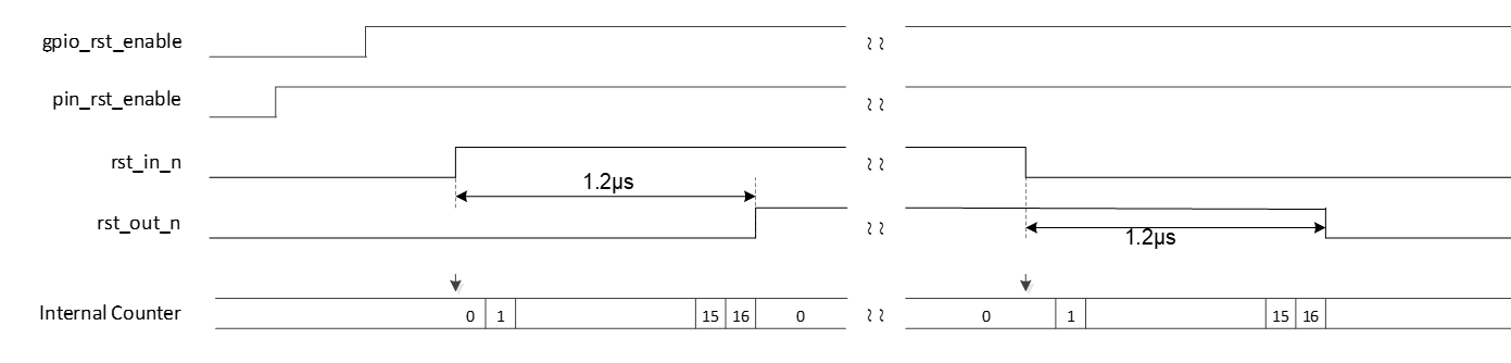
In this use case, circuitry has two enable signals; pin_rst_enable and gpio_rst_enable. The pin_rst_enable is an enable signal from external circuitry and the gpio_rst_enable is an enable control signal by software. When both signals are enabled, the circuitry is active.
The rst_in_n is an external reset input with active high, and rst_out_n is a reset output with active high. The circuitry monitors rst_in_n. When rst_in_n is activated for a specific number of continuous cycles, the rst_out_n is output. A reset will be activated or released, when the operation clock selected by CLOCK_SRC [12:8] is input continuously for 16 cycles. The source clock 80 MHz is divided by 6 to 13 MHz. Then, count 76 ns multiplied by 16 cycle, the time of reset activation or release is approximately 1.2 μs.
The following I/O port and HSIOM signals are used:
- io_data_in [6] = pin_rst_enable; (from I/O port)
- io_data_in [7] = rst_in_n; (from I/O port)
- smartio_data [5] = rst_out_n; (to I/O port)
- chip_data [4] = gpio_rst_enable; (from HSIOM)
Figure 15 shows the connection and functional logic of each LUT3 [3:0] and DU in this circuity.
Figure 15. Logical Example of a Reset Detection/Stability Circuitry

In this use case, four LUT3s and one DU are used.
LUT3 [4] is used to generate the activation signal of this circuitry from two enable signals (pin_rst_enable and gpio_rst_en). LUT 3 [6] and LUT 3 [7] are used to monitor the rst_in_n state and to start the counter of the DU. LUT 3 [5] detects the stabilization wait completion and outputs rst_out_n.
DU is used to generate reset stability wait time, and the Tr_out of LUT3 [5] is output synchronously by gated output mode.
Figure 16 shows the signal path of this use case.
Figure 16. Signal Path of Reset Detection/Stability Circuitry

In this use case, io_data_in [7:6], chip_data [4] and smartio_data [5] are used as input or output signals. Therefore, it can be configured with four LUT3s (LUT3 [7:4]). If smartio_data [3] is used for rst_out_n, it is necessary to go through LUT3 [3]. That is, five LUT3 [x] are required for this case.
Table 17, Table 18, Table 19, and Table 20 show truth table of each LUT3. The bold highlights in the tables indicate an invalid combination pattern.
Table 17. Look Up Table LUT3 [6]
Tr2_in | Tr1_in | Tr0_in | Tr_out |
|---|---|---|---|
0 | 0 | 0 | 1 |
0 | 0 | 1 | 1 |
0 | 1 | 0 | 1 |
0 | 1 | 1 | 1 |
1 | 0 | 0 | 1 |
1 | 0 | 1 | 1 |
1 | 1 | 0 | 1 |
1 | 1 | 1 | 0 |
Table 18. Look Up Table LUT3 [7]
Tr2_in | Tr1_in | Tr0_in | Tr_out |
|---|---|---|---|
0 | 0 | 0 | 0 |
0 | 0 | 1 | 0 |
0 | 1 | 0 | 0 |
0 | 1 | 1 | 1 |
1 | 0 | 0 | 0 |
1 | 0 | 1 | 1 |
1 | 1 | 0 | 0 |
1 | 1 | 1 | 0 |
Table 19. Look Up Table LUT3 [5]
Tr2_in | Tr1_in | Tr0_in | Tr_out |
|---|---|---|---|
0 | 0 | 0 | 0 |
0 | 0 | 1 | 0 |
0 | 1 | 0 | 0 |
0 | 1 | 1 | 0 |
1 | 0 | 0 | 0 |
1 | 0 | 1 | 1 |
1 | 1 | 0 | 1 |
1 | 1 | 1 | 0 |
Table 20. Look Up Table LUT3 [4]
Tr2_in | Tr1_in | Tr0_in | Tr_out |
|---|---|---|---|
0 | 0 | 0 | 0 |
0 | 0 | 1 | 0 |
0 | 1 | 0 | 0 |
0 | 1 | 1 | 0 |
1 | 0 | 0 | 0 |
1 | 0 | 1 | 0 |
1 | 1 | 0 | 0 |
1 | 1 | 1 | 1 |
LUT3 [6] is an inverter circuit with one input and one output, and each input of Tr0_in, Tr1_in and Tr2_in is the same signal. Therefore, valid combination pattern of [Tr0_in, Tr1_in, Tr2_in, Tr_out] is [0, 0, 0, 1] or [1, 1, 1, 0]. If an invalid pattern occurs, the counter circuit is reset and rst_out_n keeps the current value.
LUT3 [7] has three different inputs. If the enable signal (Tr0_in) from LUT3 [4] is valid (=“1”) and the rst_in_n state (Tr2_in) is different from rst_out_n state (Tr1_in) from LUT3 [5], “1” is output.
LUT3 [5] generates rst_out_n signal. When the enable signal (Tr2_in) from LUT3 [4] is valid (=”1”) and the stability done signal (Tr0_in) from DU is detected (stabilization wait time has passed), the current rst_out_n signal (Tr1_in, Tr_out) of LUT3 [5] is reversed.
LUT3 [4] generates the enable signal for this circuitry. It has two inputs; pin_rst_enable and gpio_rst_enable. The pin_rst_enable is input to Tr2_in, and the gpio_rst_enable is input to Tr0_in and Tr1_in. Therefore, different value combination of Tr0_in and Tr1_in are invalid pattern. If an invalid pattern occurs, the circuitry is disabled (Tr_out = “0”).
DU operates in the INCR_WRAP mode. This mode increments data by 1 from an initial value (DATA 0) until it reaches a final value (DATA 1). When the count value matches the final value, it wraps around to DATA 0. If rst is “1”, the counter value is set to initial value.
In this mode, DU has two control signal inputs; count_en and count_rst. The count_en is the input to Tr1_in, and the count_rst is input to Tr0_in. DU has two counter control registers (DATA 0 and DATA 1) and one output signal (Tr_out). DATA0 register is the initial value of the counter, and DATA1 register is final counter value.
Table 21 shows DU configuration and input/output operation.
Table 21. DU operation
Tr0_in (rst) | Tr1_in (en) | Operation | DATA 0 (Initial value) | DATA 1 (Final value) | Tr_out |
|---|---|---|---|---|---|
1 | 0 | INCR_WRAP:Increments data by 1 from an initial value (DATA 0) until it reaches a final value (DATA 1). When count value matches the final value, it wraps around to DATA 0. | 0 | 16 | 0 (It is the reset state) |
0 | 1 | A single clock pulse is output when the count value is equal to the final value. |
Tr0_in operates as “rst” and Tr1_in operates as “en”. Tr0_in is connected to the output of LUT3 [6] and Tr1_in is connected to the input of LUT3 [6]. When "1" is input to en, the DU starts a counter. Then, outputs the single pulse, when counter value reaches the final value.
Figure 17 shows the setting procedure for Smart I/O.
Figure 17. Setting procedure for Smart I/O

(1) See the Application Note for the GPIO configuration (AN220193).
(6) See the Table 20 for setting pattern.
(7) See the Table 19 for setting pattern.
(8) See the Table 17 for setting pattern.
(9) See the Table 18 for setting pattern.
Configuration and example code
Table 22 lists the parameters and Table 23 lists the functions of the configuration part in SDL for Smart I/O.
Table 22. List of Smart I/O Configuration Parameters
Parameters | Description | Value |
|---|---|---|
SMART_IO_CLK_ACTIVE | Defines Smart I/O clock source | 1ul (Select Active clock source) |
CY_SMARTIO_CLK_INV | Defines Smart I/O clock | PCLK_SMARTIO13_CLOCK |
SMART_IO_PORT | Defines Smart IO port | SMARTIO_PRT13 (It is assigned to Smar I/O Port13) |
SMARTIO_BYPASS_CH_MASK | Defines Bypass channel mask io_data_in [7] to smartio_data [7]: No bypass io_data_in [6] to smartio_data [6]: No bypass io_data_in [5] to smartio_data [5]: No bypass io_data_in [4] to smartio_data [4]: No bypass io_data_in [3] to smartio_data [3]: Bypass io_data_in [2] to smartio_data [2]: Bypass io_data_in [1] to smartio_data [1]: Bypass io_data_in [0] to smartio_data [0]: Bypass | 0x0Ful (See Table 1) No use Smart IO for io_data_in [3] to io_data_in [0] |
SMARTIO_IOSYNC_CH_MASK | Defines IO sync channel mask | 0x00ul (See Table 3) |
GPIO_RST_EN_PORT | Defines input port for LUT3[4] input | GPIO_PRT13 (It is assigned to GPIO Port13) |
GPIO_RST_EN_PIN | Defines input port pin for LUT3[4] input | 4ul (It is assigned to GPIO Port 4pin) |
GPIO_RST_EN_PIN_MUX | Configures input port pin function | P13_4_GPIO (It is assigned to GPIO) |
PIN_RST_EN_PORT | Defines input port for LUT3[6] input | GPIO_PRT13 (It is assigned to GPIO Port13) |
PIN_RST_EN_PIN | Defines input port pin for LUT3[6] input | 6ul (It is assigned to GPIO Port 6 pin) |
PIN_RST_EN_PIN_MUX | Configures input port pin function | P13_6_GPIO (It is assigned to GPIO) |
RST_IN_PORT | Defines input port for LUT3[7] input | GPIO_PRT13 (It is assigned to GPIO Port 13) |
RST_IN_PIN | Defines input port pin for LUT3[7] input | 7ul (It is assigned to GPIO Port 6 pin) |
RST_IN_PIN_MUX | Configures input port pin function | P13_7_GPIO (It is assigned to GPIO) |
RST_OUT_PORT | Defines input port for LUT3[5] output | GPIO_PRT13 (It is assigned to GPIO Port 13) |
RST_OUT_PIN | Defines input port pin for LUT3[5] output | 5ul (It is assigned to GPIO Port 6 pin) |
RST_OUT_PIN_MUX | Configures input port pin function | P13_5_GPIO (It is assigned to GPIO) |
LUT4_OUT_MAP | LUT3[4] output pattern | 0x80ul (See Table 20) |
LUT5_OUT_MAP | LUT3[5] output pattern | 0x60ul (See Table 19) |
LUT6_OUT_MAP | LUT3[6] output pattern | 0x7Ful (See Table 17) |
LUT7_OUT_MAP | LUT3[7] output pattern | 0x28ul (See Table 18) |
LUTx_LOGIC_OPCODE_COMB | Selects LUT3 Operation Mode | CY_SMARTIO_LUTOPC_COMB (It is assigned to Combinatorial) |
LUTx_LOGIC_OPCODE_GO | Selects LUT3 Operation Mode | CY_SMARTIO_LUTOPC_GATED_OUT |
LUTx_LOGIC_OPCODE_GI2 | Selects LUT3 Operation Mode | CY_SMARTIO_LUTOPC_GATED_TR2 |
CY_SYSCLK_DIV_16_BIT | Selects Divider Type to 16-bit divider | 1ul |
CY_SMARTIO_ENABLE | Sets to Smart I/O and Pipeline enable | 1ul |
CY_SMARTIO_DISABLE | Sets to Smart I/O and Pipeline Disable | 0ul |
CY_SMARTIO_DEINIT | Resets the Smart I/O to default value | 0ul |
CY_SMARTIO_CHANNEL_ALL | Sets to all pin Smart I/O bypass | 0xfful |
CY_SMARTIO_CLK_DIVACT | Selects the source clock to clk_smartio/rst_sys_act_n. See Table 2. | 16ul |
CY_SMARTIO_CLK_GATED | Selects the source clock to Clock source is a constant ‘0’. See Table 2. | 20ul |
CY_SMARTIO_CLK_ASYNC | Selects the source clock to asynchronous mode/“1”. See Table 2. | 31ul |
CY_SMARTIO_LUTTR_CHIP4 | LUT3[4] Tr0/Tr1 input | 4ul (It is assigned to LUT3[4]. See Table 6) |
CY_SMARTIO_LUTTR_IO6 | LUT3[4] Tr2 input | 14ul (It is assigned to LUT3[4]. See Table 6) |
CY_SMARTIO_LUTTR_DU_OUT | LUT3[5] Tr0 input | 0ul (It is assigned to LUT3[5]. See Table 6) |
CY_SMARTIO_LUTTR_LUT5_OUT | LUT3[5] Tr1 input/LUT3[7] Tr1 input | 5ul (It is assigned to LUT3[5]. See Table 6) |
CY_SMARTIO_LUTTR_LUT4_OUT | LUT3[5] Tr2 input/ LUT3[7] Tr2 input | 4ul (It is assigned to LUT3[5]. See Table 6) |
CY_SMARTIO_LUTTR_LUT7_OUT | LUT3[6] Tr0/Tr1/Tr2 input | 7ul (It is assigned to LUT3[6]. See Table 6) |
CY_SMARTIO_LUTTR_IO7 | LUT3[7] Tr0 input | 15ul (It is assigned to LUT3[7]. See Table 6) |
CY_SMARTIO_DUTR_LUT6_OUT | DU Tr0 input trigger source | 9ul (It is assigned to LUT6 output. See Table 9) |
CY_SMARTIO_DUTR_LUT7_OUT | DU Tr1 input trigger source | 10ul (It is assigned to LUT7 output. See Table 9) |
CY_SMARTIO_DUTR_ZERO | DU Tr2 input trigger source | 0ul (It is assigned to Constant 0. See Table 9) |
CY_SMARTIO_DUDATA_ZERO | DU data0 input DATA source | 0ul (It is assigned to Constant 0. See Table 10) |
CY_SMARTIO_DUDATA_DATAREG | DU data1 input DATA source | 3ul (It is assigned to SMARTIO.DATA register. See Table 10) |
CY_SMARTIO_DUOPC_INCR_WRAP | DU opcode | 3ul (It is assigned to Increment and wrap-around (Count up and wrap). See Table 11) |
CY_SMARTIO_DUSIZE_8 | DU operation bit size | 7ul (It is assigned to 8-bits size/width operand. See Table 10) |
smart_io_cfg.clkSrc | Source clock setting | CY_SMARTIO_CLK_DIVACT |
smart_io_cfg.bypassMask | Configures bypass setting | SMARTIO_BYPASS_CH_MASK |
smart_io_cfg.ioSyncEn | Configures Synchronizer setting | SMARTIO_IOSYNC_CH_MASK |
lutCfgLut4.opcode | Configures LUT3[4] Operation Mode setting | LUTx_LOGIC_OPCODE_GI2 |
lutCfgLut4.lutMap | Configures LUT3[4] output pattern setting | LUT4_OUT_MAP |
lutCfgLut4.tr0 | Configures LUT3[4] tr0 input | CY_SMARTIO_LUTTR_CHIP4 |
lutCfgLut4.tr1 | Configures LUT3[4] tr1 input | CY_SMARTIO_LUTTR_CHIP4 |
lutCfgLut4.tr2 | Configures LUT3[4] tr2 input | CY_SMARTIO_LUTTR_IO6 |
lutCfgLut5.opcode | Configures LUT3[5] Operation Mode setting | LUTx_LOGIC_OPCODE_GO |
lutCfgLut5.lutMap | Configures LUT3[5] output pattern setting | LUT5_OUT_MAP |
lutCfgLut5.tr0 | Configures LUT3[5] tr0 input | CY_SMARTIO_LUTTR_DU_OUT |
lutCfgLut5.tr1 | Configures LUT3[5] tr1 input | CY_SMARTIO_LUTTR_LUT5_OUT |
lutCfgLut5.tr2 | Configures LUT3[5] tr2 input | CY_SMARTIO_LUTTR_LUT4_OUT |
lutCfgLut6.opcode | Configures LUT3[6] Operation Mode setting | LUTx_LOGIC_OPCODE_COMB |
lutCfgLut6.lutMap | Configures LUT3[6] output pattern setting | LUT6_OUT_MAP |
lutCfgLut6.tr0 | Configures LUT3[6] tr0 input | CY_SMARTIO_LUTTR_LUT7_OUT |
lutCfgLut6.tr1 | Configures LUT3[6] tr1 input | CY_SMARTIO_LUTTR_LUT7_OUT |
lutCfgLut6.tr2 | Configures LUT3[6] tr2 input | CY_SMARTIO_LUTTR_LUT7_OUT |
lutCfgLut7.opcode | Configures LUT3[7] Operation Mode setting | LUTx_LOGIC_OPCODE_GI2 |
lutCfgLut7.lutMap | Configures LUT3[7] output pattern setting | LUT7_OUT_MAP |
lutCfgLut7.tr0 | Configures LUT3[7] tr0 input | CY_SMARTIO_LUTTR_LUT4_OUT |
lutCfgLut7.tr1 | Configures LUT3[7] tr1 input | CY_SMARTIO_LUTTR_LUT5_OUT |
lutCfgLut7.tr2 | Configures LUT3[7] tr2 input | CY_SMARTIO_LUTTR_IO7 |
lutCfgDu.tr0 | Configures DU input trigger 0 source selection - LUT[3]6 output | CY_SMARTIO_DUTR_LUT6_OUT |
lutCfgDu.tr1 | Configures DU input trigger 1 source selection - LUT[3]7 output | CY_SMARTIO_DUTR_LUT7_OUT |
lutCfgDu.tr2 | Configures DU input trigger 2 source selection - Constant 0 | CY_SMARTIO_DUTR_ZERO |
lutCfgDu.data0 | DU input DATA0 source selection - Fixed 0 | CY_SMARTIO_DUDATA_ZERO |
lutCfgDu.data1 | DU input DATA1 source selection - SMARTIO_PRTx_DATA.DATA [7:0] | CY_SMARTIO_DUDATA_DATAREG |
lutCfgDu.opcode | DU op-code | CY_SMARTIO_DUOPC_INCR_WRAP |
lutCfgDu.size | DU width size is 8 | CY_SMARTIO_DUSIZE_8 |
lutCfgDu.dataReg | DU DATA register value = 16 | 10ul |
sourceFreq | Source Frequency | 80000000ul (80MHz) |
targetFreq | Target Frequency | 12000000ul (12MHz) |
Table 23. List of Smart I/O configuration functions
Functions | Description | Remarks |
|---|---|---|
Init_IO_Pin() | Configures GPIO Port pin | – |
Cy_SmartIO_Deinit() | Resets the Smart I/O to default values | Resets the Smart I/O registers; SMARTIO_PRTx_CTL, SMARTIO_PRTx_SYNC_CTL, SMARTIO_PRTx_LUT_SELy, SMARTIO_PRTx_LUT_CTLy, SMARTIO_PRTx_DU_SEL, SMARTIO_PRTx_DU_CTL and SMARTIO_PRTx_DATA |
Init_SmartIO() | Configures and enables Smart I/O, Calls for Init_SmartIO_Cfg() and Cy_SmartIO_Enable() | – |
Init_SmartIO_Cfg() | Configures Smart I/O setting structure, Calls for Cy_SmartIO_Init() | – |
Cy_SmartIO_Enable() | Enable Smart I/O | Write to PIPELINE_EN and ENABLED bit |
Cy_SmartIO_Init() | Configures Smart I/O register | Write to the related registers for Source clock, Bypass, Synchronizer, LUT3, and DU. |
Code Listing 8 demonstrates an example program to reset detection/stability circuitry. See the Architecture TRM and Application Note for GPIO and clock configuration.
The following description will help you understand the register notation of the driver part of SDL:
- base signifies the pointer to the Smart I/O register base address.
- base- >unLUT_SEL[idx].u32Register is the SMARTIO_PRTx_LUT_SEL[idx] register mentioned in the Registers TRM. Other registers are also described in the same manner. “ x ” signifies the port suffix number and “ idx ” signifies the register index number.
- To improve the register setting performance, the SDL writes a complete 32-bit data to the register. Each bit field is generated and written to the register as the final 32-bit data.
    un_SMARTIO_PRT_CTL_t workCTL= {.u32Register = 0ul};
    workCTL.stcField.u1ENABLED     = CY_SMARTIO_DISABLE;
    workCTL.stcField.u1PIPELINE_EN = CY_SMARTIO_ENABLE;
    workCTL.stcField.u5CLOCK_SRC   = CY_SMARTIO_CLK_GATED;
    workCTL.stcField.u8BYPASS      = CY_SMARTIO_CHANNEL_ALL;
    base->unCTL.u32Register        = workCTL.u32Register;
See cyip_smartio_v2.h under hdr/rev_x/ip for more information on the union and structure representation of registers.
Code Listing 8 Example to Reset Detection/Stability Circuitry
    /* Smart IO clock source selection */
    /* Define Clock active */
    #define SMART_IO_CLK_ACTIVE             1ul

    /* Smart IO port selections macro */
    /* Define Smart I/O port */
    #define SMART_IO_PORT                   SMARTIO_PRT13

    /* Define Smart I/O Clock */
    #define CY_SMARTIO_CLK_INV              PCLK_SMARTIO13_CLOCK

    /* Bypass channel mask */
    /* Define Smart I/O bypass channel */
    #define SMARTIO_BYPASS_CH_MASK          0x0Ful /* 00001111: 0000 means [7:4] are not bypassed i.e. programmable SMARTIO is exposed */

    /* IO sync channel mask */
    /* Define Smart I/O sync channel */
    #define SMARTIO_IOSYNC_CH_MASK          0x00ul

    /* Lut pin configuration */
    /* Define input port to LUT3[4] */
    #define GPIO_RST_EN_PORT                GPIO_PRT13
    #define GPIO_RST_EN_PIN                 4ul
    #define GPIO_RST_EN_PIN_MUX             P13_4_GPIO /* Check signal at BB JP6.7 */

    /* Define input port to LUT3[6] */
    #define PIN_RST_EN_PORT                 GPIO_PRT13
    #define PIN_RST_EN_PIN                  6ul
    #define PIN_RST_EN_PIN_MUX              P13_6_GPIO /* Check signal at BB JP11.14 */

    /* Define input port to LUT3[7] */
    #define RST_IN_PORT                     GPIO_PRT13
    #define RST_IN_PIN                      7ul
    #define RST_IN_PIN_MUX                  P13_7_GPIO /* Check signal at BB JP11.13 */

    /* Define output port to LUT3[5] */
    #define RST_OUT_PORT                    GPIO_PRT13
    #define RST_OUT_PIN                     5ul
    #define RST_OUT_PIN_MUX                 P13_5_GPIO /* Check signal at BB JP6.6 */

    /* LUT output map */
    /* Define LUT3[4], LUT3[5], LUT3[6] and LUT3[7] output pattern */
    #define LUT4_OUT_MAP                    0x80ul
    #define LUT5_OUT_MAP                    0x28ul
    #define LUT6_OUT_MAP                    0x7Ful
    #define LUT7_OUT_MAP                    0x28ul

    /* LUT logic circuit type macro */
    /* Define LUT logic circuit type */
    #define LUTx_LOGIC_OPCODE_COMB          CY_SMARTIO_LUTOPC_COMB
    #define LUTx_LOGIC_OPCODE_GO            CY_SMARTIO_LUTOPC_GATED_OUT
    #define LUTx_LOGIC_OPCODE_GI2           CY_SMARTIO_LUTOPC_GATED_TR2

    #define CY_SMARTIO_ENABLE  1ul
    #define CY_SMARTIO_DISABLE 0ul
    #define CY_SMARTIO_DEINIT  0ul
    #define CY_SMARTIO_CHANNEL_ALL  0xfful   /**< All channels */

    /* Port pin configuration */
    /******************************************************************************/

    /* Configure Port for output (Port13 pin) */
    cy_stc_gpio_pin_config_t gpio_rst_cfg =
    {
        .outVal    = 0ul,
        .driveMode = CY_GPIO_DM_STRONG_IN_OFF, /* SmartIO from CPU */
        .hsiom     = GPIO_RST_EN_PIN_MUX,      /* P13_4_GPIO */
        .intEdge   = 0ul,
        .intMask   = 0ul,
        .vtrip     = 0ul,
        .slewRate  = 0ul,
        .driveSel  = 0ul,
    };

    /* Configure Port for input (Port13 pin) */
    cy_stc_gpio_pin_config_t pin_rst_cfg =
    {
        .outVal    = 0ul,
        .driveMode = CY_GPIO_DM_HIGHZ,         /* CPU from SmartIO */
        .hsiom     = PIN_RST_EN_PIN_MUX,       /* P13_6_GPIO */
        .intEdge   = 0ul,
        .intMask   = 0ul,
        .vtrip     = 0ul,
        .slewRate  = 0ul,
        .driveSel  = 0ul,
    };

    /* Configure Port for input (Port13 pin) */
    cy_stc_gpio_pin_config_t rst_in_cfg =
    {
        .outVal    = 0ul,
        .driveMode = CY_GPIO_DM_HIGHZ,         /* CPU from SmartIO */
        .hsiom     = RST_IN_PIN_MUX,           /* P13_7_GPIO */
        .intEdge   = 0ul,
        .intMask   = 0ul,
        .vtrip     = 0ul,
        .slewRate  = 0ul,
        .driveSel  = 0ul,
    };

    /* Configure Port for output (Port13 pin) */
    cy_stc_gpio_pin_config_t rst_out_cfg =
    {
        .outVal    = 0ul,
        .driveMode = CY_GPIO_DM_STRONG_IN_OFF, /* CPU from SmartIO */
        .hsiom     = RST_OUT_PIN_MUX,          /* P13_5_GPIO */
        .intEdge   = 0ul,
        .intMask   = 0ul,
        .vtrip     = 0ul,
        .slewRate  = 0ul,
        .driveSel  = 0ul,
    };


    int main(void)
    {
        :
        Init_IO_Pin();   /* (1) Configure GPIO pin. See Code Listing 9. */

        /* Deinit before Init */
        Cy_SmartIO_Deinit(SMART_IO_PORT);   /* Disable all Smart I/O. See Code Listing 10. */

        /* SmartIO peripheral clock divider setting */
        /* (3) Configure peripheral Clock */
        {
            Cy_SysClk_PeriphAssignDivider(CY_SMARTIO_CLK_INV, CY_SYSCLK_DIV_16_BIT, 0ul);
            uint32_t sourceFreq = 80000000ul;
            uint32_t targetFreq = 12000000ul;
            uint32_t divNum = (sourceFreq / targetFreq);

            Cy_SysClk_PeriphSetDivider(CY_SYSCLK_DIV_16_BIT, 0ul, (divNum - 1ul));
            Cy_SysClk_PeriphEnableDivider(CY_SYSCLK_DIV_16_BIT, 0ul);
        }

        Init_SmartIO();    /* Initialize Smart I/O. See Code Listing 11. */

        Cy_SysEnableApplCore(CY_CORTEX_M4_APPL_ADDR);

        Cy_GPIO_Clr(GPIO_PRT13, 4ul);

        while(1)
        {

        }
    }
Code Listing 9 Init_IO_Pin() Function
   void Init_IO_Pin(void)
   {
       /* Please check ReadMe.txt for proper connection of Input and Output */
       /* Configure Port13 4pin. */
       Cy_GPIO_Pin_Init(GPIO_RST_EN_PORT, GPIO_RST_EN_PIN, &gpio_rst_cfg);

       /* Configure Port13 pin */
       Cy_GPIO_Pin_Init(PIN_RST_EN_PORT, PIN_RST_EN_PIN, &pin_rst_cfg);

       /* Configure Port13 pin */
       Cy_GPIO_Pin_Init(RST_IN_PORT, RST_IN_PIN, &rst_in_cfg);

       /* Configure Port13 pin */
       Cy_GPIO_Pin_Init(RST_OUT_PORT, RST_OUT_PIN, &rst_out_cfg);
   }
Code Listing 10 Cy_SmartIO_Deinit() Function
    void Cy_SmartIO_Deinit(volatile stc_SMARTIO_PRT_t* base)
    {
        un_SMARTIO_PRT_CTL_t workCTL= {.u32Register = 0ul};
        workCTL.stcField.u1ENABLED     = CY_SMARTIO_DISABLE;   /* (2) Disable all Smart I/O port */
        workCTL.stcField.u1PIPELINE_EN = CY_SMARTIO_ENABLE;
        workCTL.stcField.u5CLOCK_SRC   = CY_SMARTIO_CLK_GATED;
        workCTL.stcField.u8BYPASS      = CY_SMARTIO_CHANNEL_ALL;
        base->unCTL.u32Register        = workCTL.u32Register;

        base->unSYNC_CTL.u32Register = CY_SMARTIO_DEINIT;
        for(uint8_t idx = CY_SMARTIO_LUTMIN; idx < CY_SMARTIO_LUTMAX; idx++)
        {
            base->unLUT_SEL[idx].u32Register = CY_SMARTIO_DEINIT;
            base->unLUT_CTL[idx].u32Register = CY_SMARTIO_DEINIT;
        }
        base->unDU_SEL.u32Register = CY_SMARTIO_DEINIT;
        base->unDU_CTL.u32Register = CY_SMARTIO_DEINIT;
        base->unDATA.u32Register = CY_SMARTIO_DEINIT;
    }
Code Listing 11 Init_SmartIO() Function
    void Init_SmartIO(void)
    {
        cy_en_smartio_status_t retStatus = (cy_en_smartio_status_t)0xFF;

    /* Configure Smart I/O. See Code Listing 12. */
        retStatus = Init_SmartIO_Cfg();
        if(retStatus == CY_SMARTIO_SUCCESS)
        {
            /* After all the configuration, enable SMART IO */
            /* Enable Smart I/O. See Code Listing 13. */
            Cy_SmartIO_Enable(SMART_IO_PORT);
        }
    }
Code Listing 12 Init_SmartIO_Cfg() Function
   cy_en_smartio_status_t Init_SmartIO_Cfg(void)
   {
       cy_stc_smartio_ducfg_t lutCfgDu;
       cy_stc_smartio_lutcfg_t lutCfgLut4;
       cy_stc_smartio_lutcfg_t lutCfgLut5;
       cy_stc_smartio_lutcfg_t lutCfgLut6;
       cy_stc_smartio_lutcfg_t lutCfgLut7;

       cy_stc_smartio_config_t smart_io_cfg;
       cy_en_smartio_status_t retStatus = (cy_en_smartio_status_t)0xFF;

       /* initialize the Smart IO structure */
       /* Clear configuration structure */
       memset(&lutCfgDu, 0ul, sizeof(cy_stc_smartio_ducfg_t));
       memset(&lutCfgLut4, 0ul, sizeof(cy_stc_smartio_lutcfg_t));
       memset(&lutCfgLut5, 0ul, sizeof(cy_stc_smartio_lutcfg_t));
       memset(&lutCfgLut6, 0ul, sizeof(cy_stc_smartio_lutcfg_t));
       memset(&lutCfgLut7, 0ul, sizeof(cy_stc_smartio_lutcfg_t));
       memset(&smart_io_cfg, 0ul, sizeof(cy_stc_smartio_config_t));

   #ifdef SMART_IO_CLK_ACTIVE
       /* Active clock source is selected */
       /* Configure Smart I/O clock source */
       smart_io_cfg.clkSrc = (cy_en_smartio_clksrc_t)CY_SMARTIO_CLK_DIVACT;
   #else
       /* Asynchronous clock source is selected */
       smart_io_cfg.clkSrc = (cy_en_smartio_clksrc_t)CY_SMARTIO_CLK_ASYNC;
   #endif  /* SMART_IO_CLK_ACTIVE */

       /* Bypass channel mask for input and output pin */
       /* Configure BYPASS setting */
       smart_io_cfg.bypassMask = SMARTIO_BYPASS_CH_MASK;

       /* IO channel sync mask for selected pin */
       /* Configure Synchronizer setting */
       smart_io_cfg.ioSyncEn = SMARTIO_IOSYNC_CH_MASK;

       /*************************** LUT3[4] setting ***************************/
       /* Configure LUT3 [4] */
       lutCfgLut4.opcode = LUTx_LOGIC_OPCODE_GI2;
       lutCfgLut4.lutMap = LUT4_OUT_MAP;

       /* Lut configuration for input */
       lutCfgLut4.tr0 = (cy_en_smartio_luttr_t)CY_SMARTIO_LUTTR_CHIP4;
       lutCfgLut4.tr1 = (cy_en_smartio_luttr_t)CY_SMARTIO_LUTTR_CHIP4;
       lutCfgLut4.tr2 = (cy_en_smartio_luttr_t)CY_SMARTIO_LUTTR_IO6;
       smart_io_cfg.lutCfg[4] = &lutCfgLut4;

       /*************************** LUT3[5] setting ***************************/
       /* Configure LUT3 [5] */
       /* Lut configuration for output, check description above */
       lutCfgLut5.opcode = LUTx_LOGIC_OPCODE_GO;
       lutCfgLut5.lutMap = LUT5_OUT_MAP;

       /* Lut configuration for input (button) */
       lutCfgLut5.tr0 = (cy_en_smartio_luttr_t)CY_SMARTIO_LUTTR_DU_OUT;
       lutCfgLut5.tr1 = (cy_en_smartio_luttr_t)CY_SMARTIO_LUTTR_LUT5_OUT;
       lutCfgLut5.tr2 = (cy_en_smartio_luttr_t)CY_SMARTIO_LUTTR_LUT4_OUT;
       smart_io_cfg.lutCfg[5] = &lutCfgLut5;

       /*************************** LUT3[6] setting ***************************/
       /* Configure LUT3 [6] */
       lutCfgLut6.opcode = LUTx_LOGIC_OPCODE_COMB;
       lutCfgLut6.lutMap = LUT6_OUT_MAP;

       /* Lut configuration for input */
       lutCfgLut6.tr0 = (cy_en_smartio_luttr_t)CY_SMARTIO_LUTTR_LUT7_OUT;
       lutCfgLut6.tr1 = (cy_en_smartio_luttr_t)CY_SMARTIO_LUTTR_LUT7_OUT;
       lutCfgLut6.tr2 = (cy_en_smartio_luttr_t)CY_SMARTIO_LUTTR_LUT7_OUT;
       smart_io_cfg.lutCfg[6] = &lutCfgLut6;

       /*************************** LUT3[7] setting ***************************/
       /* Configure LUT3 [7] */
       lutCfgLut7.opcode = LUTx_LOGIC_OPCODE_GI2;
       lutCfgLut7.lutMap = LUT7_OUT_MAP;

       /* Lut configuration for input */
       lutCfgLut7.tr0 = (cy_en_smartio_luttr_t)CY_SMARTIO_LUTTR_LUT4_OUT;
       lutCfgLut7.tr1 = (cy_en_smartio_luttr_t)CY_SMARTIO_LUTTR_LUT5_OUT;
       lutCfgLut7.tr2 = (cy_en_smartio_luttr_t)CY_SMARTIO_LUTTR_IO7;
       smart_io_cfg.lutCfg[7] = &lutCfgLut7;

       /*************************** DU setting ***************************/
       /* Configure DU */
       lutCfgDu.tr0 = CY_SMARTIO_DUTR_LUT6_OUT;        /**< DU input trigger 0 source selection - LUT[3]6 output*/
       lutCfgDu.tr1 = CY_SMARTIO_DUTR_LUT7_OUT;        /**< DU input trigger 1 source selection - LUT[3]7 output*/
       lutCfgDu.tr2 = CY_SMARTIO_DUTR_ZERO;            /**< DU input trigger 2 source selection - Constant 0*/
       lutCfgDu.data0 = CY_SMARTIO_DUDATA_ZERO;        /**< DU input DATA0 source selection - Fixed 0*/
       lutCfgDu.data1 = CY_SMARTIO_DUDATA_DATAREG;     /**< DU input DATA1 source selection - SMARTIO_PRTx_DATA.DATA [7:0]*/
       lutCfgDu.opcode = CY_SMARTIO_DUOPC_INCR_WRAP;   /**< DU op-code */
       lutCfgDu.size = CY_SMARTIO_DUSIZE_8;            /**< DU width size is 8 */
       lutCfgDu.dataReg = 0x10ul;                      /**< DU DATA register value = 16 */
       smart_io_cfg.duCfg = &lutCfgDu;

       /*****************************************************************/
       /* Initialization of Smart IO structure */
       /* Configure Smart I/O. See Code Listing 14. */
       retStatus = Cy_SmartIO_Init(SMART_IO_PORT, &smart_io_cfg);
       return retStatus;
   }
Code Listing 13 Cy_SmartIO_Enable() Function
    void Cy_SmartIO_Enable(volatile stc_SMARTIO_PRT_t* base)
    {
        un_SMARTIO_PRT_CTL_t workCTL = base->unCTL;
        workCTL.stcField.u1ENABLED     = CY_SMARTIO_ENABLE;
        workCTL.stcField.u1PIPELINE_EN = CY_SMARTIO_DISABLE;
        base->unCTL.u32Register        = workCTL.u32Register;  /* (12) Enable Smart I/O. */
    }
Code Listing 14 Cy_SmartIO_Init() Function
    cy_en_smartio_status_t Cy_SmartIO_Init(volatile stc_SMARTIO_PRT_t* base, const cy_stc_smartio_config_t* config)
    {
        cy_en_smartio_status_t status = CY_SMARTIO_SUCCESS;

        if(NULL != config)
        {
            /* (4) Set clock source and bypass to Smart IO */
            un_SMARTIO_PRT_CTL_t workCTL = {.u32Register = 0ul};
            workCTL.stcField.u1ENABLED     = CY_SMARTIO_DISABLE;
            workCTL.stcField.u1HLD_OVR     = config->hldOvr;
            workCTL.stcField.u1PIPELINE_EN = CY_SMARTIO_ENABLE;
            workCTL.stcField.u5CLOCK_SRC   = config->clkSrc;
            workCTL.stcField.u8BYPASS      = config->bypassMask;
            base->unCTL.u32Register        = workCTL.u32Register;

            /* (5) Set synchronizer to Smart IO */
            un_SMARTIO_PRT_SYNC_CTL_t workSYNC_CTL = {.u32Register = 0ul};
            workSYNC_CTL.stcField.u8IO_SYNC_EN   = config->ioSyncEn;
            workSYNC_CTL.stcField.u8CHIP_SYNC_EN = config->chipSyncEn;
            base->unSYNC_CTL.u32Register         = workSYNC_CTL.u32Register;

            /* LUT configurations - skip if lutCfg is a NULL pointer */
            /* (6), (7), (8), (9) Set LUT3 */
            for(uint32_t i = CY_SMARTIO_LUTMIN; i < CY_SMARTIO_LUTMAX; i++)
            {
                if(NULL != config->lutCfg[i])
                {
                    un_SMARTIO_PRT_LUT_SEL_t workLUT_SET = { .u32Register = 0ul };
                    workLUT_SET.stcField.u4LUT_TR0_SEL = config->lutCfg[i]->tr0;
                    workLUT_SET.stcField.u4LUT_TR1_SEL = config->lutCfg[i]->tr1;
                    workLUT_SET.stcField.u4LUT_TR2_SEL = config->lutCfg[i]->tr2;
                    base->unLUT_SEL[i].u32Register     = workLUT_SET.u32Register;

                    un_SMARTIO_PRT_LUT_CTL_t workLUT_CTL = { .u32Register = 0ul };
                    workLUT_CTL.stcField.u2LUT_OPC = config->lutCfg[i]->opcode;
                    workLUT_CTL.stcField.u8LUT     = config->lutCfg[i]->lutMap;
                    base->unLUT_CTL[i].u32Register = workLUT_CTL.u32Register;
                }
            }

            /* DU Configuration - skip if duCfg is a NULL pointer */
            /* (10) Set DU */
            if(NULL != config->duCfg)
            {
                un_SMARTIO_PRT_DU_SEL_t workDU_SEL = {.u32Register = 0ul};
                workDU_SEL.stcField.u4DU_TR0_SEL   = config->duCfg->tr0;
                workDU_SEL.stcField.u4DU_TR1_SEL   = config->duCfg->tr1;
                workDU_SEL.stcField.u4DU_TR2_SEL   = config->duCfg->tr2;
                workDU_SEL.stcField.u2DU_DATA0_SEL = config->duCfg->data0;
                workDU_SEL.stcField.u2DU_DATA1_SEL = config->duCfg->data1;
                base->unDU_SEL.u32Register         = workDU_SEL.u32Register;

                un_SMARTIO_PRT_DU_CTL_t workDU_CTL = {.u32Register = 0ul};
                workDU_CTL.stcField.u3DU_SIZE = config->duCfg->size;
                workDU_CTL.stcField.u4DU_OPC  = config->duCfg->opcode;
                base->unDU_CTL.u32Register    = workDU_CTL.u32Register;

                base->unDATA.stcField.u8DATA = config->duCfg->dataReg;
            }
        }
        Else
        {
            status = CY_SMARTIO_BAD_PARAM;
        }

        return(status);
    }
Glossary
Terms | Description |
|---|---|
chip_data | Input signals from HSIOM |
Clk_sys/CLK_HF | This is derived from the system clock using a peripheral clock divider. See the Clocking System chapter of the Architecture TRM for details. |
DeepSleep | Power mode that only low-frequency peripherals are available. See the DeepSleep Mode section in the Device Power Modes chapter of the Architecture TRM for details. |
DU | Data Unit. DU performs simple increment, decrement, increment/decrement, shift, and AND/OR operations based on opcode configuration in register. See the Smart I/O - Data Unit section in the I/O System chapter of the Architecture TRM for details. |
GPIO | General-purpose input/output |
HSIOM | High Speed I/O Matrix. See the High-Speed I/O Matrix section in the I/O System chapter of the Architecture TRM for details. |
io_data_in | Input signals from I/O port |
I/O Port | I/O Port provides the interface between the CPU core and peripheral components to the outside world. See the I/O System chapter of the Architecture TRM for details. |
LUT3 [x] | 3-input Lookup Tables. LUT3 [x] block takes three input signals and generates an output based on the configuration set in register. See the Smart I/O - LUT3 section in the I/O System chapter of the Architecture TRM for details. |
smartio_data | Output signals from Smart I/O |
Related Documents
The following are the TRAVEO™ T2G family series datasheets and Technical Reference Manuals. Contact Technical Support to obtain these documents.
- Device datasheet
- CYT2B7 Datasheet 32-Bit Arm® Cortex®-M4F Microcontroller TRAVEO™ T2G family
- CYT2B9 Datasheet 32-Bit Arm® Cortex®-M4F Microcontroller TRAVEO™ T2G family
- CYT4BF Datasheet 32-Bit Arm® Cortex®-M7 Microcontroller TRAVEO™ T2G family
- CYT4DN Datasheet 32-Bit Arm® Cortex®-M7 Microcontroller TRAVEO™ T2G family
- CYT3BB/4BB Datasheet 32-Bit Arm® Cortex®-M7 Microcontroller TRAVEO™ T2G family
- Body Controller Entry Family
- TRAVEO™ T2G Automotive Body Controller Entry Family Architecture Technical Reference Manual (TRM)
- TRAVEO™ T2G Automotive Body Controller Entry Registers Technical Reference Manual (TRM) for CYT2B7
- TRAVEO™ T2G Automotive Body Controller Entry Registers Technical Reference Manual (TRM) for CYT2B9
- Body Controller High Family
- TRAVEO™ T2G Automotive Body Controller High Family Architecture Technical Reference Manual (TRM)
- TRAVEO™ T2G Automotive Body Controller High Registers Technical Reference Manual (TRM) for CYT4BF
- TRAVEO™ T2G Automotive Body Controller High Registers Technical Reference Manual (TRM) for CYT3BB/4BB
- Cluster 2D Family
- TRAVEO™ T2G Automotive Cluster 2d Family Architecture Technical Reference Manual (TRM)
- TRAVEO™ T2G Automotive Cluster 2d Registers Technical Reference Manual (TRM)
- Application Note
- AN220193 - GPIO USAGE SETUP IN TRAVEO™ T2G FAMILY
- AN220208 - CLOCK CONFIGURATION SETUP IN TRAVEO™ T2G BODY ENTRY FAMILY
- AN224434 - CLOCK CONFIGURATION SETUP IN TRAVEO™ T2G FAMILY CYT4B SERIES
- AN226071 - CLOCK CONFIGURATION SETUP IN TRAVEO™ T2G FAMILY CYT4D SERIES
- AN229513 - CLOCK CONFIGURATION SETUP IN TRAVEO™ T2G FAMILY CYT2C SERIES
Other references
A Sample Driver Library (SDL) including startup as sample software to access various peripherals is provided. SDL also serves as a reference, to customers, for drivers that are not covered by the official AUTOSAR products. The SDL cannot be used for production purposes as it does not qualify to any automotive standards. The code snippets in this application note are part of the SDL. Contact Technical Support to obtain the SDL.
Revision history
Document version | Date of release | Description of changes |
|---|---|---|
** | 2018-09-27 | New application note. |
*A | 2019-06-17 | Updated Associated Part Family as “TRAVEO™ T2G family CYT2B/CYT4B Series”. Added target part numbers “CYT4B Series” related information in all instances across the document. |
*B | 2019-11-20 | Updated Associated Part Family as “TRAVEO™ T2G family CYT2B/CYT4B/CYT4D Series”. Added target part numbers “CYT4D Series” related information in all instances across the document. |
*C | 2020-06-29 | Updated Associated Part Family as “TRAVEO™ T2G family CYT2/CYT3/CYT4 Series”. Changed target part numbers from “CYT2B/CYT4B/CYT4D Series” to “CYT2/CYT4 Series” in all instances across the document. Added target part numbers “CYT3 Series” in all instances across the document. |
*D | 2021-04-16 | Updated Example Configuration: Added example of SDL Code and description in all instances. Updated to Infineon template. |
*E | 2023-11-10 | Template update; no content updated. |
1 Subscripts x in register names used in this sentence are Port number
2 Subscripts y in register names used in this sentence are LUT3 number.