AN219755 Using a SAR ADC in TRAVEO™ T2G automotive microcontrollers
About this document
Scope and purpose
This application note demonstrates how to configure and use a SAR ADC in TRAVEO™ T2G automotive microcontrollers with a software trigger, a hardware trigger, group processing, averaging, range detection, pulse detection, diagnosis, and calibration.
Intended audience
This document is intended for anyone who uses the SAR ADC of the TRAVEO™ T2G automotive microcontrollers.
Associated part family
TRAVEO™ T2G family
Introduction
This application note describes how to use a SAR ADC for Infineon TRAVEO™ T2G automotive microcontrollers. The SAR ADC converts analog input voltages into digital values. The analog channels can be an individual or grouped. Each channel can be triggered by software or hardware. The SAR ADC features averaging, range detection, pulse detection and diagnosis and calibration.
In general, the ADC result is affected by the environment, such as power supply voltage, reference voltage, input analog voltage, temperature, and noise. Therefore, calibration and averaging of the multiple ADC results are recommended to mitigate the influence of the environment.
To understand the functionality described and terminology used in this application note, see the “SAR ADC” chapter of the architecture technical reference manual (TRM)
Software trigger procedure
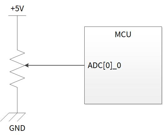
Figure 1 shows an example application that converts the given voltage values to pin ADC[0]_0 of the MCU to digital values. Analog-to-digital conversion is repeated in the interrupt service routine by using a software trigger.
Figure 1. Example of analog-to-digital conversion connection
To implement this application, use the following sections that describe the procedure for setting the ADC channel. These sections also provide an example for using a software trigger.
Basic ADC global settings
This section describes how to configure the ADC based on a use case using the sample driver library (SDL). The code snippets in this application note are part of SDL. See Other references.
SDL has a configuration part and a driver part. The configuration part configures the parameter values for the desired operation. The driver part configures each register based on the parameter values in the configuration part. You can configure the configuration part according to your system.
ADC global settings
The following are the procedures to configure common ADC settings in each channel:
- ADC enable and auto idle power down setting by the SARn_CTL register
- Debug freeze setting by the PASS_PASS_CTL register
Figure 2 shows an example of the ADC global settings.
Figure 2. Example of ADC global settings

Use case
The following use case is an example of ADC global setting:
- ADC logical channel: 0
- ADC operation frequency: 26.67 MHz
- Auto idle power down: 0 (Disable)
- Power-up time: 0 (Disable)
- SAR IP: 1 (Enable)
- SAR ADC and SARSEQ: 1(Enable)
- SARMUX: 1 (Enable)
Configuration
Table 1 lists the parameters and Table 2 lists the functions of the configuration part of in SDL for ADC global settings.
Table 1. List of ADC global settings parameters
Parameters | Description | Value |
|---|---|---|
| Analog macro for the potentiometer on the TRAVEO™ T2G baseboard | CY_ADC_POT_MACRO: PASS0_SAR0 |
| Bad parameter was passed | 0x01ul |
| Freezes ADC0 in debug mode | 0ul |
| Freezes ADC1 in debug mode | 0ul |
| Freezes ADC2 in debug mode | 0ul |
| Freezes ADC3 in debug mode | 0ul |
| Pre-condition time | 0ul |
| Power-up time | 0ul |
| Enables idle power down | false |
| MSB stretch mode 0: CY_ADC_MSB_STRETCH_MODE_1CYCLE 1: CY_ADC_MSB_STRETCH_MODE_2CYCLE | 1ul |
| Enables the half-LSB conversion | 0ul |
| Enables SAR MUX | true |
| Enables ADC | true |
| Enables SAR IP | true |
Table 2. List of ADC global settings functions
Functions | Description | Value |
|---|---|---|
| Initializes the ADC module | PASS SAR = BB_POTI_ANALOG_MACRO ADC Configure = adcConfig |
Sample code
This section demonstrates a sample code for the initial configuration of ADC global settings. The following description will help you understand the register notation of the driver part of the SDL:
-
base->unENABLE.stcField.u1CHAN_EN is the PASS0_SAR0_CH0_ENABLE.CHAN_EN setting mentioned in the registers TRM. Other registers are also described in the same manner.
-
Performance improvement measures: To improve the performance of register setting, the SDL writes a complete 32-bit data to the register. Each bit field is generated in advance in a bit-writable buffer and written to the register as the final 32-bit data.
unPostCtl.u32Register = base->unPOST_CTL.u32Register; unPostCtl.stcField.u3POST_PROC = config->postProcessingMode; unPostCtl.stcField.u1LEFT_ALIGN = config->resultAlignment; unPostCtl.stcField.u1SIGN_EXT = config->signExtention; unPostCtl.stcField.u8AVG_CNT = config->averageCount; unPostCtl.stcField.u5SHIFT_R = config->rightShift; unPostCtl.stcField.u2RANGE_MODE = config->rangeDetectionMode; unPostCtl.stcField.u5SHIFT_R = config->rightShift; unPostCtl.stcField.u2RANGE_MODE = config->rangeDetectionMode; base->unPOST_CTL.u32Register = unPostCtl.u32Register;
See cyip_pass.h under hdr/rev_x/ip for more information on the union and structure representation of registers.
Code Listing 1 General configuration of ADC global settings
    :
    #define BB_POTI_ANALOG_MACRO        CY_ADC_POT_MACRO
    :
    /* Control freeze feature for debugging. */
    cy_stc_adc_debug_freeze_config_t FreezeConfig =
    {
        /* If true, freeze ADC0 in debug mode. */
        .enableFreezeAdc0 = 0ul,
        .enableFreezeAdc1 = 0ul,
        .enableFreezeAdc2 = 0ul,
        .enableFreezeAdc3 = 0ul,
    };
    :
    int main(void)
    {
    :
        __enable_irq(); /* Enable global interrupts. */

       /* Initialize ADC */
        {
            cy_stc_adc_config_t adcConfig =  /* ADC Configuration.*/
            {
                .preconditionTime    = 0ul,
                .powerupTime         = 0ul,
                .enableIdlePowerDown = false,
                .msbStretchMode      = CY_ADC_MSB_STRETCH_MODE_2CYCLE,
                .enableHalfLsbConv   = 0ul,
                .sarMuxEnable        = true,
                .adcEnable           = true,
                .sarIpEnable         = true,
            };
            Cy_Adc_Init(BB_POTI_ANALOG_MACRO, &adcConfig);  /* ADC Initialize. See Code Listing 2. */
            Cy_Adc_SetDebugFreezeMode(PASS0_EPASS_MMIO,&FreezeConfig);  /* Set Debug freeze mode. See Code Listing 3. */
    :
       }
    :
        for(;;)
        {
        }
    }
Code Listing 2 Cy_Adc_Init() function
    cy_en_adc_status_t Cy_Adc_Init(volatile stc_PASS_SAR_t * base, const cy_stc_adc_config_t * config)
    {
        cy_en_adc_status_t ret = CY_ADC_SUCCESS;
        un_PASS_SAR_CTL_t unSarCtl = { 0 };
        if (NULL != config)
        {
            /* CTL register setting */
            base->unPRECOND_CTL.stcField.u4PRECOND_TIME = config->preconditionTime;

            /* CTL register setting */  /* (1) Enable DC Setting. Auto Idle Power Down Setting. */
            unSarCtl.stcField.u8PWRUP_TIME  = config->powerupTime;
            unSarCtl.stcField.u1IDLE_PWRDWN = config->enableIdlePowerDown ? 1ul : 0ul;
            unSarCtl.stcField.u1MSB_STRETCH = config->msbStretchMode;
            unSarCtl.stcField.u1HALF_LSB    = config->enableHalfLsbConv ? 1ul : 0ul;
            unSarCtl.stcField.u1SARMUX_EN   = config->sarMuxEnable ? 1ul : 0ul;
            unSarCtl.stcField.u1ADC_EN      = config->adcEnable ? 1ul : 0ul;
            unSarCtl.stcField.u1ENABLED     = config->sarIpEnable ? 1ul : 0ul;
            base->unCTL.u32Register         = unSarCtl.u32Register;
        }
        else
        {
            ret = CY_ADC_BAD_PARAM;
        }

        return ret;
    }
Code Listing 3 Cy_Adc_SetDebugFreezeMode () function
    cy_en_adc_status_t Cy_Adc_SetDebugFreezeMode(volatile stc_PASS_EPASS_MMIO_t * base, const cy_stc_adc_debug_freeze_config_t * config)
    {
        cy_en_adc_status_t ret  = CY_ADC_SUCCESS;
        uint32_t           temp = 0ul;
        if (NULL != config)
        {
            temp |= (config->enableFreezeAdc0) ? 1ul : 0ul;
            temp |= (config->enableFreezeAdc1) ? 2ul : 0ul;
            temp |= (config->enableFreezeAdc2) ? 4ul : 0ul;
            temp |= (config->enableFreezeAdc3) ? 8ul : 0ul;
            base->unPASS_CTL.stcField.u4DBG_FREEZE_EN = temp;  /* (2) Debug Freeze disabled by default. */
        }
        else
        {
            ret = CY_ADC_BAD_PARAM;
        }
        return ret;
    }
Logical channel settings with software trigger
Each logical channel has one A/D conversion result register. A logical channel can be assigned as any analog input (ADC[n]_i) by setting the SARn_CHx_SAMPLE_CTL register.
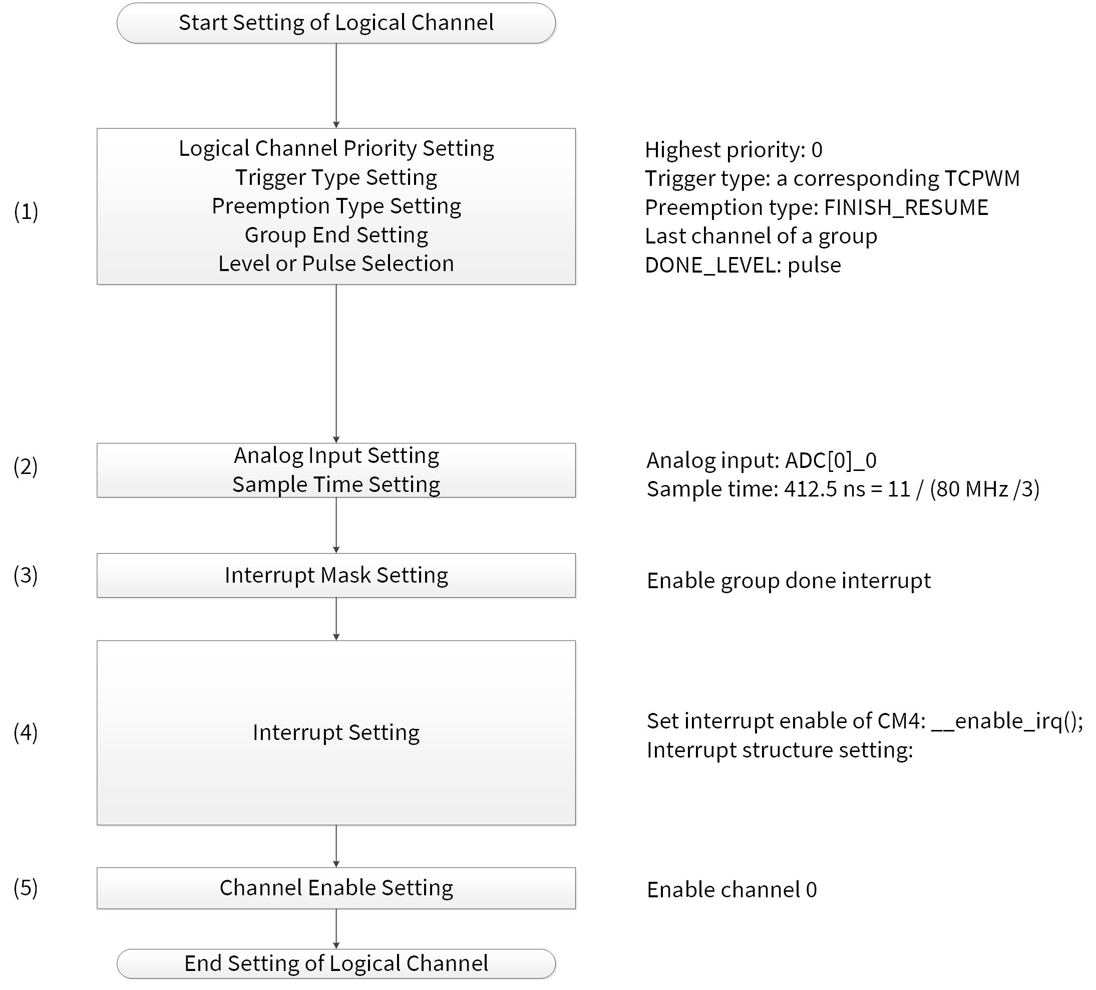
Figure 3 shows the example of logical channel setting with a software trigger. In this example, the minimum value of the sample time is used. To find the proper sample time for your system, see the datasheet mentioned in Related documents.
Figure 3. Example of logical channel setting with software trigger

Logical channel 0 is used in this example. Any logical channel will work in this application if a proper analog input is selected.
Use case
The following use case is an example of logical channel setting with software trigger.
- Analog input: ADC[0]_0
- Sample time: 412.5 ns = 11 / (80 MHz /3)
- ADC trigger selection: OFF
- Channel priority: 0 (highest)
- Channel pre-emption type: Finish resume
- Channel group: The last channel
- ADC done level: Pulse
- ADC pin/port address: ADC[0]_0
- External analog MUX: 0, Enable
- Pre-conditioning mode: OFF
- Overlap diagnostics mode: OFF
- Calibration value select: Regular
- Post processing mode: None
- Result alignment: Right
- Sign extension: Unsigned
- Averaging count: 0
- Shift right: 0
- Mask group: Done/Not cancelled/Not overflow
- Mask channel: Not range/Not pulse/Not overflow
Configuration
Table 3 lists the parameters and Table 4 lists the functions of the configuration part of in SDL for logical channel settings with software trigger.
Table 3. Logical channel settings with software trigger parameters
Parameters | Description | Value |
|---|---|---|
| Analog macro for the potentiometer on the TRAVEO™ T2G baseboard | CY_ADC_POT_MACRO: PASS0_SAR0 |
| Analog input number for the potentiometer on the TRAVEO™ T2G baseboard | CH0 (CH[ADC_LOGICAL_CHANNEL]) |
| MSB stretch mode | 1ul (See Table 1) |
| Trigger OFF 0: CY_ADC_TRIGGER_OFF 1: CY_ADC_TRIGGER_TCPWM 2: CY_ADC_TRIGGER_GENERIC0 3: CY_ADC_TRIGGER_GENERIC1 4: CY_ADC_TRIGGER_GENERIC2 5: CY_ADC_TRIGGER_GENERIC3 6: CY_ADC_TRIGGER_GENERIC4 7: CY_ADC_TRIGGER_CONTINUOUS | 0ul |
| Channel priority | 0ul |
| Pre-emption type 0: CY_ADC_PREEMPTION_ABORT_CANCEL 1: CY_ADC_PREEMPTION_ABORT_RESTART 2: CY_ADC_PREEMPTION_ABORT_RESUME 3: CY_ADC_PREEMPTION_FINISH_RESUME | 3ul |
| Is group end? | true |
| Done level 0: CY_ADC_DONE_LEVEL_PULSE 1: CY_ADC_DONE_LEVEL_LEVEL | 0ul |
| Pin address | BB_POTI_ANALOG_INPUT_NO |
| Port address 0: CY_ADC_PORT_ADDRESS_SARMUX0 1: CY_ADC_PORT_ADDRESS_SARMUX1 2: CY_ADC_PORT_ADDRESS_SARMUX2 3: CY_ADC_PORT_ADDRESS_SARMUX3 | 0ul |
| External MUX select | 0ul |
| Enables external MUX | true |
| Pre-condition mode 0: CY_ADC_PRECONDITION_MODE_OFF 1: CY_ADC_PRECONDITION_MODE_VREFL 2: CY_ADC_PRECONDITION_MODE_VREFH 3: CY_ADC_PRECONDITION_MODE_DIAG | 0ul |
| Overlap diagnostics mode 0: CY_ADC_OVERLAP_DIAG_MODE_OFF 1: CY_ADC_OVERLAP_DIAG_MODE_HALF 2: CY_ADC_OVERLAP_DIAG_MODE_FULL 3: CY_ADC_OVERLAP_DIAG_MODE_MUX_DIAG | 0ul |
| Sample time | samplingCycle (Calculated Value) |
| Calibration value select 0: CY_ADC_CALIBRATION_VALUE_REGULAR 1: CY_ADC_CALIBRATION_VALUE_ALTERNATE | 0ul |
| Post-processing mode 0: CY_ADC_POST_PROCESSING_MODE_NONE 1: CY_ADC_POST_PROCESSING_MODE_AVG 2: CY_ADC_POST_PROCESSING_MODE_AVG_RANGE 3: CY_ADC_POST_PROCESSING_MODE_RANGE 4: CY_ADC_POST_PROCESSING_MODE_RANGE_PULSE | 0ul |
| Result alignment 0: CY_ADC_RESULT_ALIGNMENT_RIGHT 1: CY_ADC_RESULT_ALIGNMENT_LEFT | 0ul |
| Sign extension 0: CY_ADC_SIGN_EXTENTION_UNSIGNED 1: CY_ADC_SIGN_EXTENTION_SIGNED | 0ul |
| Average count | 0ul |
| Right shift | 0ul |
| Range detection mode 0: CY_ADC_RANGE_DETECTION_MODE_BELOW_LO 1: CY_ADC_RANGE_DETECTION_MODE_INSIDE_RANGE 2: CY_ADC_RANGE_DETECTION_MODE_ABOVE_HI 3: CY_ADC_RANGE_DETECTION_MODE_OUTSIDE_RANGE | 1ul |
| Range detection low threshold | 0x0000ul |
| Range detection high threshold | 0x0FFFul |
| Mask group done | true |
| Mask group cancelled | false |
| Mask group overflow | false |
| Mask channel range | false |
| Mask channel pulse | false |
| Mask channel overflow | false |
Table 4. Functions for logical channel settings with software trigger
Functions | Description | Value |
|---|---|---|
| Initializes the ADC channel | PASS SARchannel = &BB_POTI_ANALOG_MACRO->CH[ADC_LOGICAL_CHANNEL] ADCchannel Configure = adcChannelConfig |
| Sets the ADC channel interrupt mask | PASS SARchannel = base INTR Source = mask |
| Initializes the referenced system interrupt by setting the interrupt vector | Config = irq_cfg |
| Enables the corresponding channel | SARchannel = PASS_SAR_CH |
| Issues a software start trigger | PASS SARchannel = &BB_POTI_ANALOG_MACRO->CH[ADC_LOGICAL_CHANNEL] |
Sample code
See Code Listing 4 to Code Listing 9 for sample code for initial configuration of logical channel settings with software trigger settings.
Code Listing 4 General configuration of ADC global settings
    :
    #define BB_POTI_ANALOG_MACRO        CY_ADC_POT_MACRO
    #define BB_POTI_ANALOG_INPUT_NO    ((cy_en_adc_pin_address_t)CY_ADC_POT_IN_NO)
    :
    int main(void)
    {
    :
        __enable_irq(); /* Enable global interrupts. */

       /* Initialize ADC */
        {
    :
            cy_stc_adc_config_t adcConfig =  /* ADC Configuration.*/
            {
                .preconditionTime    = 0ul,
                .powerupTime         = 0ul,
                .enableIdlePowerDown = false,
                .msbStretchMode      = CY_ADC_MSB_STRETCH_MODE_2CYCLE,
                .enableHalfLsbConv   = 0ul,
                .sarMuxEnable        = true,
                .adcEnable           = true,
                .sarIpEnable         = true,
            };
            cy_stc_adc_channel_config_t adcChannelConfig =
            {
                .triggerSelection          = CY_ADC_TRIGGER_OFF,  /* Trigger type setting */
                .channelPriority           = 0ul,  /* (1) Logical channel priority setting */
                .preenptionType            = CY_ADC_PREEMPTION_FINISH_RESUME,  /* Preemption type setting */
                .isGroupEnd                = true,  /* Group End setting */
                .doneLevel                 = CY_ADC_DONE_LEVEL_PULSE,  /* Level or pulse selection  */
                .pinAddress                = BB_POTI_ANALOG_INPUT_NO,  /* (2) Analog input setting, Sample time setting */
                .portAddress               = CY_ADC_PORT_ADDRESS_SARMUX0,  /* (2) Analog input setting, Sample time setting */
                .extMuxSelect              = 0ul,  /* (2) Analog input setting, Sample time setting */
                .extMuxEnable              = true,  /* (2) Analog input setting, Sample time setting */
                .preconditionMode          = CY_ADC_PRECONDITION_MODE_OFF,  /* (2) Analog input setting, Sample time setting */
                .overlapDiagMode           = CY_ADC_OVERLAP_DIAG_MODE_OFF,  /* (2) Analog input setting, Sample time setting */
                .sampleTime                = 0ul,   /* (2) Analog input setting, Sample time setting */
                .calibrationValueSelect    = CY_ADC_CALIBRATION_VALUE_REGULAR,  /* (2) Analog input setting, Sample time setting */
                .postProcessingMode        = CY_ADC_POST_PROCESSING_MODE_NONE,  /* (2) Analog input setting, Sample time setting */
                .resultAlignment           = CY_ADC_RESULT_ALIGNMENT_RIGHT,  /* (2) Analog input setting, Sample time setting */
                .signExtention             = CY_ADC_SIGN_EXTENTION_UNSIGNED,  /* (2) Analog input setting, Sample time setting */
                .averageCount              = 0ul,  /* (2) Analog input setting, Sample time setting */
                .rightShift                = 0ul,  /* (2) Analog input setting, Sample time setting */
                .rangeDetectionMode        = CY_ADC_RANGE_DETECTION_MODE_INSIDE_RANGE,
                .rangeDetectionLoThreshold = 0x0000ul,  /* Continuation of (2) */
                .rangeDetectionHiThreshold = 0x0FFFul,  /* Continuation of (2) */
                .mask.grpDone              = true,  /* (3) Interrupt mask setting */
                .mask.grpCancelled         = false,  /* (3) Interrupt mask setting */
                .mask.grpOverflow          = false,  /* (3) Interrupt mask setting */
                .mask.chRange              = false,  /* (3) Interrupt mask setting */
                .mask.chPulse              = false,  /* (3) Interrupt mask setting */
                .mask.chOverflow           = false,  /* (3) Interrupt mask setting */
            };


            Cy_Adc_Init(BB_POTI_ANALOG_MACRO, &adcConfig);  /* ADC Initialize. See Code Listing 2 */
            Cy_Adc_Channel_Init(&BB_POTI_ANALOG_MACRO->CH[ADC_LOGICAL_CHANNEL], &adcChannelConfig);  /* Initialize ADC Channel. See Code Listing 5. */
        }

    :
            Cy_SysInt_InitIRQ(&irq_cfg);  /* Initialize Interrupt Request. See Code Listing 7 */

    :
        /* Enable ADC ch. */  /* Enable ADC Channel. See Code Listing 8 */
        Cy_Adc_Channel_Enable(&BB_POTI_ANALOG_MACRO->CH[ADC_LOGICAL_CHANNEL]);
        /* Issue SW trigger */
        Cy_Adc_Channel_SoftwareTrigger(&BB_POTI_ANALOG_MACRO->CH[ADC_LOGICAL_CHANNEL]);  /* Software Trigger Setting. See Code Listing 9 */
        for(;;)
        {
        }
    }
Code Listing 5 Cy_Adc_Channel_Init() function
    cy_en_adc_status_t Cy_Adc_Channel_Init(volatile stc_PASS_SAR_CH_t * base, const cy_stc_adc_channel_config_t * config)
    {
        cy_en_adc_status_t          ret         = CY_ADC_SUCCESS;
        un_PASS_SAR_CH_TR_CTL_t     unTrCtl     = { 0ul };
        un_PASS_SAR_CH_SAMPLE_CTL_t unSampleCtl = { 0ul };
        un_PASS_SAR_CH_POST_CTL_t   unPostCtl   = { 0ul };
        un_PASS_SAR_CH_RANGE_CTL_t  unRangeCtl  = { 0ul };
        un_PASS_SAR_CH_INTR_t       unIntr      = { 0ul };

        if (NULL != config)
        {
    :
            /* Clear whole interrupt flags */
            unIntr.stcField.u1CH_OVERFLOW       = 1ul;
            unIntr.stcField.u1CH_PULSE          = 1ul;
            unIntr.stcField.u1CH_RANGE          = 1ul;
            unIntr.stcField.u1GRP_CANCELLED     = 1ul;
            unIntr.stcField.u1GRP_DONE          = 1ul;
            unIntr.stcField.u1GRP_OVERFLOW      = 1ul;
            base->unINTR.u32Register            = unIntr.u32Register;

            unTrCtl.stcField.u3SEL              = config->triggerSelection;
            unTrCtl.stcField.u3PRIO             = config->channelPriority;
            unTrCtl.stcField.u2PREEMPT_TYPE     = config->preenptionType;
            unTrCtl.stcField.u1GROUP_END        = config->isGroupEnd ? 1ul : 0ul;
            unTrCtl.stcField.u1DONE_LEVEL       = config->doneLevel ? 1ul : 0ul;
            base->unTR_CTL.u32Register          = unTrCtl.u32Register;

            unSampleCtl.stcField.u6PIN_ADDR     = config->pinAddress;
            unSampleCtl.stcField.u2PORT_ADDR    = config->portAddress;
            unSampleCtl.stcField.u3EXT_MUX_SEL  = config->extMuxSelect;
            unSampleCtl.stcField.u1EXT_MUX_EN   = config->extMuxEnable ? 1ul : 0ul;
            unSampleCtl.stcField.u2PRECOND_MODE = config->preconditionMode;
            unSampleCtl.stcField.u2OVERLAP_DIAG = config->overlapDiagMode;
            unSampleCtl.stcField.u12SAMPLE_TIME = config->sampleTime;
            unSampleCtl.stcField.u1ALT_CAL      = config->calibrationValueSelect;
            base->unSAMPLE_CTL.u32Register      = unSampleCtl.u32Register;

            unPostCtl.stcField.u3POST_PROC      = config->postProcessingMode;
            unPostCtl.stcField.u1LEFT_ALIGN     = config->resultAlignment;
            unPostCtl.stcField.u1SIGN_EXT       = config->signExtention;
            unPostCtl.stcField.u8AVG_CNT        = config->averageCount;
            unPostCtl.stcField.u5SHIFT_R        = config->rightShift;
            unPostCtl.stcField.u2RANGE_MODE     = config->rangeDetectionMode;
            base->unPOST_CTL.u32Register        = unPostCtl.u32Register;

            unRangeCtl.stcField.u16RANGE_LO     = config->rangeDetectionLoThreshold;
            unRangeCtl.stcField.u16RANGE_HI     = config->rangeDetectionHiThreshold;
            base->unRANGE_CTL.u32Register       = unRangeCtl.u32Register;

            Cy_Adc_Channel_SetInterruptMask(base, &config->mask);  /* ADC Channel Set Interrupt Mask. See Code Listing 6 */
        }
        else
        {
            ret = CY_ADC_BAD_PARAM;
        }
        return ret;
    }
Code Listing 6 Cy_Adc_Channel_SetInterruptMask() function
  cy_en_adc_status_t Cy_Adc_Channel_SetInterruptMask(volatile stc_PASS_SAR_CH_t * base, const cy_stc_adc_interrupt_source_t * mask)
  {
      cy_en_adc_status_t ret = CY_ADC_SUCCESS;
      un_PASS_SAR_CH_INTR_MASK_t unMask = { 0ul };
      if (NULL != mask)
      {
          unMask.stcField.u1CH_OVERFLOW_MASK   = mask->chOverflow   ? 1ul : 0ul;
          unMask.stcField.u1CH_PULSE_MASK      = mask->chPulse      ? 1ul : 0ul;
          unMask.stcField.u1CH_RANGE_MASK      = mask->chRange      ? 1ul : 0ul;
          unMask.stcField.u1GRP_CANCELLED_MASK = mask->grpCancelled ? 1ul : 0ul;
          unMask.stcField.u1GRP_DONE_MASK      = mask->grpDone      ? 1ul : 0ul;
          unMask.stcField.u1GRP_OVERFLOW_MASK  = mask->grpOverflow  ? 1ul : 0ul;
          base->unINTR_MASK.u32Register        = unMask.u32Register;
      }
      else
      {
          ret = CY_ADC_BAD_PARAM;
      }
      return ret;
  }
Code Listing 7 Cy_SysInt_InitIRQ() function
    cy_en_sysint_status_t Cy_SysInt_InitIRQ(const cy_stc_sysint_irq_t* config)
    {
        cy_en_sysint_status_t status = CY_SYSINT_SUCCESS;

        #if (CY_CPU_CORTEX_M0P)
            un_CPUSS_CM0_SYSTEM_INT_CTL_t unIntCtl = { 0ul };
        #else
            #if defined (tviibe512k) || defined (tviibe1m) || defined (tviibe2m)|| defined (tviibe4m)
                un_CPUSS_CM4_SYSTEM_INT_CTL_t unIntCtl = { 0ul };
            #elif defined (tviibh4m) || defined (tviibh8m) || defined (tviic2d6m) || defined (tviic2d4m) || defined (tviic2d6mddr)
                un_CPUSS_CM7_0_SYSTEM_INT_CTL_t unIntCtl0 = { 0ul };
                un_CPUSS_CM7_1_SYSTEM_INT_CTL_t unIntCtl1 = { 0ul };
            #endif
        #endif
        if(NULL != config)
        {
            #if (CY_CPU_CORTEX_M0P) //rmkn u3CM0_CPU_INT_IDX->u3CPU_INT_IDX
                #if defined (tviibe512k) || defined (tviibe1m) || defined (tviibe2m)|| defined (tviibe4m)
                    unIntCtl.stcField.u3CPU_INT_IDX = (uint8_t)config->intIdx;
                #elif defined (tviibh4m) || defined (tviibh8m) || defined (tviic2d6m) || defined (tviic2d4m) || defined (tviic2d6mddr)
                    unIntCtl.stcField.u3CM0_CPU_INT_IDX = (uint8_t)config->intIdx;
                #endif
                unIntCtl.stcField.u1CPU_INT_VALID = config->isEnabled ? 1ul : 0ul;
                CPUSS->unCM0_SYSTEM_INT_CTL[config->sysIntSrc].u32Register = unIntCtl.u32Register;
            #else
                #if defined (tviibe512k) || defined (tviibe1m) || defined (tviibe2m)|| defined (tviibe4m)
                    unIntCtl.stcField.u3CPU_INT_IDX = (uint8_t)config->intIdx;
                    unIntCtl.stcField.u1CPU_INT_VALID = config->isEnabled ? 1ul : 0ul;
                    CPUSS->unCM4_SYSTEM_INT_CTL[config->sysIntSrc].u32Register = unIntCtl.u32Register;  /* (4) Set Interrupt Enable of CM4, Interrupt structure setting, Priority setting, Clear pending status and Enable IRQ. */
                #elif defined (tviibh4m) || defined (tviibh8m) || defined (tviic2d6m) || defined (tviic2d4m) || defined (tviic2d6mddr)
                    if(CPUSS->unIDENTITY.stcField.u4MS == CPUSS_MS_ID_CM7_0)
                    {
                        unIntCtl0.stcField.u4CPU_INT_IDX = (uint8_t)config->intIdx;
                        unIntCtl0.stcField.u1CPU_INT_VALID = config->isEnabled ? 1ul : 0ul;
                        CPUSS->unCM7_0_SYSTEM_INT_CTL[config->sysIntSrc].u32Register = unIntCtl0.u32Register;
                    }
                    else // should be CPUSS_MS_ID_CM7_1
                    {
                        unIntCtl1.stcField.u4CPU_INT_IDX = (uint8_t)config->intIdx;
                        unIntCtl1.stcField.u1CPU_INT_VALID = config->isEnabled ? 1ul : 0ul;
                        CPUSS->unCM7_1_SYSTEM_INT_CTL[config->sysIntSrc].u32Register = unIntCtl1.u32Register;
                    }
                #endif
            #endif
        }
        else
        {
            status = CY_SYSINT_BAD_PARAM;
        }

        return(status);
    }
Code Listing 8 Cy_Adc_Channel_Enable() function
   void Cy_Adc_Channel_Enable(volatile stc_PASS_SAR_CH_t * base)
   {
       base->unENABLE.stcField.u1CHAN_EN = 1ul;  /* (5) Enable Channel 0. */
   }
Code Listing 9 Cy_Adc_Channel_SoftwareTrigger() function
    void Cy_Adc_Channel_SoftwareTrigger(volatile stc_PASS_SAR_CH_t * base)
    {
        base->unTR_CMD.stcField.u1START = 1ul;  /* (6) Enable Software Trigger. */
    }
A/D conversion ISR with software trigger
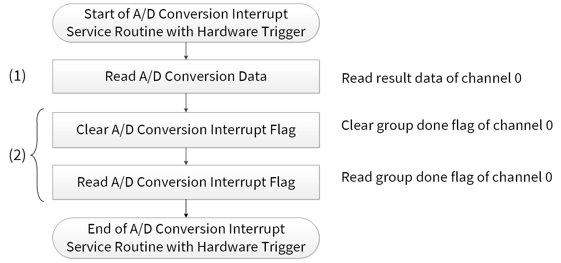
Figure 4 shows the example of ADC ISR with a software trigger. For details on CPU interrupt handling, see the architecture TRM mentioned in Related documents.
Figure 4. Example of ADC ISR with software trigger

Use case
See Section 2.3.1.
Configuration
Table 5 lists the parameters and Table 6 lists the functions of the configuration part of in SDL for ADC Global settings.
Table 5. Parameters for ADC ISR with software trigger
Parameters | Description | Value |
|---|---|---|
| Analog macro for the potentiometer on TRAVEO™ T2G baseboard | CY_ADC_POT_MACRO: PASS0_SAR0 |
| Conversion result buffer | - (Calculated Value) |
| Status result buffer | - (Calculated Value) |
| Index result | - (Calculated Value) |
| Interrupt source | - (Calculated Value) |
Table 6. Functions for ADC ISR with software trigger
Functions | Description | Value |
|---|---|---|
| Gets the conversion result and status | SAR Channel = BB_POTI_ANALOG_MACRO->CH[ADC_LOGICAL_CHANNEL], Result = resultBuff[resultIdx], Status= statusBuff[resultIdx] |
| Clears the corresponding channel interrupt status | SAR Channel = BB_POTI_ANALOG_MACRO->CH[ADC_LOGICAL_CHANNEL], Source = intrSource |
| Issues the software start trigger | SAR Channel = BB_POTI_ANALOG_MACRO->CH[ADC_LOGICAL_CHANNEL] |
Sample code
See Code Listing 10 to Code Listing 12 for sample code for initial configuration of ADC ISR with software trigger.
Code Listing 10 ADC ISR with software trigger
#define BB_POTI_ANALOG_MACRO        CY_ADC_POT_MACRO
:
uint16_t               resultBuff[16];
cy_stc_adc_ch_status_t statusBuff[16];
uint8_t                resultIdx;
:

void AdcIntHandler(void)
{
         cy_stc_adc_interrupt_source_t intrSource = { false };
:
    {
        /* Get the result(s) */  /* (1) Read A/D conversion data. See Code Listing 11. */
        Cy_Adc_Channel_GetResult(&BB_POTI_ANALOG_MACRO->CH[ADC_LOGICAL_CHANNEL], &resultBuff[resultIdx], &statusBuff[resultIdx]);

        /* Display ADC result */
        printf("\rADC result = %04d          ", resultBuff[resultIdx]);


        /* Increment result idx */
        resultIdx = (resultIdx + 1) % (sizeof(resultBuff) / sizeof(resultBuff[0]));


        /* Clear interrupt source */  /* (2) Clear and read A/D conversion flag. See Code Listing 12. */
        Cy_Adc_Channel_ClearInterruptStatus(&BB_POTI_ANALOG_MACRO->CH[ADC_LOGICAL_CHANNEL], &intrSource);

        /* Trigger next conversion */
        Cy_Adc_Channel_SoftwareTrigger(&BB_POTI_ANALOG_MACRO->CH[ADC_LOGICAL_CHANNEL]);  /* (3) Software Trigger Setting. See Code Listing 9. */
    }
    else
    {
        // Unexpected interrupt
        CY_ASSERT(false);
    }
}
Code Listing 11 Cy_Adc_Channel_GetResult() function
    Cy_Adc_Channel_GetResult(const volatile stc_PASS_SAR_CH_t * base, uint16_t * result, cy_stc_adc_ch_status_t * status)
    {
        cy_en_adc_status_t ret = CY_ADC_SUCCESS;
        un_PASS_SAR_CH_RESULT_t value;

        if ((NULL != result) && (NULL != status))
        {
            value.u32Register = base->unRESULT.u32Register;
            *result           = value.stcField.u16RESULT;
            status->aboveHi   = (value.stcField.u1ABOVE_HI_MIR   != 0ul) ? true : false;
            status->pulseIntr = (value.stcField.u1PULSE_INTR_MIR != 0ul) ? true : false;
            status->rangeIntr = (value.stcField.u1RANGE_INTR_MIR != 0ul) ? true : false;
            status->valid     = (value.stcField.u1VALID_MIR      != 0ul) ? true : false;
        }
        else
        {
            ret = CY_ADC_BAD_PARAM;
        }
        return ret;
    }
Code Listing 12 Cy_Adc_Channel_ClearInterruptStatus() function
    cy_en_adc_status_t Cy_Adc_Channel_ClearInterruptStatus(volatile stc_PASS_SAR_CH_t * base, const cy_stc_adc_interrupt_source_t * source)
    {
        cy_en_adc_status_t ret = CY_ADC_SUCCESS;
        un_PASS_SAR_CH_INTR_t unIntr = { 0ul };
        if (NULL != source)
        {
            unIntr.stcField.u1CH_OVERFLOW   = source->chOverflow   ? 1ul : 0ul;
            unIntr.stcField.u1CH_PULSE      = source->chPulse      ? 1ul : 0ul;
            unIntr.stcField.u1CH_RANGE      = source->chRange      ? 1ul : 0ul;
            unIntr.stcField.u1GRP_CANCELLED = source->grpCancelled ? 1ul : 0ul;
            unIntr.stcField.u1GRP_DONE      = source->grpDone      ? 1ul : 0ul;
            unIntr.stcField.u1GRP_OVERFLOW  = source->grpOverflow  ? 1ul : 0ul;
            base->unINTR.u32Register        = unIntr.u32Register;
        }
        else
        {
            ret = CY_ADC_BAD_PARAM;
        }
        return ret;
    }
Hardware trigger procedure
The SAR ADC can be triggered by other related hardware functions, such as TCPWM, GPIO, and event generator.
This section explains the example application that converts the voltage values given to ADC[0]_0 pin of the MCU to digital values. The analog-to-digital conversion is repeated at regular intervals by hardware trigger of a corresponding TCPWM.
The physical setting of this application is the same as shown in Figure 1.
Ensure that you have set up the parameters as mentioned in Basic ADC global settings.
To implement this application, follow the procedure of ADC channel setting and its example when using a hardware trigger. The example in this section uses a corresponding TCPWM for the trigger.
Logical channel setting with hardware trigger
Figure 5 shows the example of logical channel setting with a hardware trigger in CYT2 series. In this example, the minimum value of the sample time is used. To find the proper sample time for your system, see the datasheet mentioned in Related documents.
Figure 5. Example of logical channel setting with hardware trigger in CYT2
series
Logical channel 0 is used in this example. Any logical channel will work in this application if a proper analog input is selected. Also, TCPWM and the trigger multiplexer should be configured.
Use case
The following use case is an example of logical channel setting with hardware trigger:
- Analog input: ADC[0]_0
- Sample time: 412.5 ns = 11 / (80 MHz /3)
- Trigger select: TCPWM
- Pre-emption type: FINISH_RESUME
- GROUP_END: Last channel of a group
- External analog MUX: 0, Enable
- Pre-conditioning mode: OFF
- Overlap diagnostics mode: OFF
- Calibration value select: Regular
- Post processing mode: None
- Result alignment: Right
- Sign extension: Unsigned
- Averaging count: 0
- Shift right: 0
- Mask group: Done/Not cancelled/Not overflow
- Mask channel: Not range/Not pulse/Not overflow
Configuration
Table 7 lists the parameters and Table 8 lists the functions of the configuration part of in SDL for Logical Channel Setting with Hardware Trigger in CYT2 Series settings.
Table 7. Parameters for logical channel setting with hardware trigger
in CYT2 series
Parameters | Description | Value |
|---|---|---|
| Analog macro for the potentiometer on the TRAVEO™ T2G baseboard | CY_ADC_POT_MACRO: PASS0_SAR0 |
| Strong drive, Input buffer off | 0x06ul |
| Pin output state | 0ul |
| Drive mode | CY_GPIO_DM_STRONG_IN_OFF |
| High-speed I/O matrix selection | TCPWMx_LINEx_MUX |
| Interrupt edge type | 0ul |
| Interrupt enable mask | 0ul |
| Input buffer voltage trip type | 0ul |
| Output buffer slew rate | 0ul |
| Drive strength | 0ul |
| Analog High-Z, input buffer off | 0x00ul |
| Pin output state | 0ul |
| Drive Mode | CY_GPIO_DM_ANALOG |
| High-speed I/O matrix selection | P6_0_GPIO |
| Interrupt edge type | 0ul |
| Interrupt enable mask | 0ul |
| Input buffer voltage trip type | 0ul |
| Output buffer slew rate | 0ul |
| Drive strength | 0ul |
| Pre-condition time | 0ul |
| Power-up time | 0ul |
| Enables idle power down | false |
| MSB stretch mode | 1ul (See Table 1) |
| Enables half LSB conversion | 0ul |
| Enables SAR MUX | true |
| Enables ADC | true |
| Enables SAR IP | true |
| Trigger selection | 1ul (See Table 3) |
| Channel priority | 0ul |
| Pre-emption type | 3ul (See Table 3) |
| Is group end? | true |
| Done level | 0ul (See Table 3) |
| Pin address | BB_POTI_ANALOG_INPUT_NO |
| Port address | 0ul (See Table 3) |
| External MUX select | 0ul |
| Enable external MUX | true |
| Pre-condition mode | 0ul (See Table 3) |
| Overlap diagnostics mode | 0ul (See Table 3) |
| Sample time | 0ul |
| Calibration value select | 0ul (See Table 3) |
| Post processing mode | 0ul (See Table 3) |
| Result alignment | 0ul (See Table 3) |
| Sign extension | 0ul (See Table 3) |
| Average count | 0ul |
| Right shift | 0ul |
| Range detection mode | 1ul (See Table 3) |
| Range detection low threshold | 0x0000ul |
| Range detection high threshold | 0x0FFFul |
| Mask group done | true |
| Mask group cancelled | false |
| Mask group overflow | false |
| Mask channel range | false |
| Mask channel pulse | false |
| Mask channel overflow | false |
Table 8. Functions for logical channel setting with hardware trigger in
CYT2 series
Functions | Description | Value |
|---|---|---|
| Returns the interrupt status | PASS SARchannel = &BB_POTI_ANALOG_MACRO->CH[ADC_LOGICAL_CHANNEL] INTR Source = &intrSource |
| Changes the User ISR vector for the system interrupt | Source = sysIntSrc INTR handler = AdcIntHandler |
| Initializes all pin configuration settings for the pin | Port Number = TCPWMx_LINEx_PORT Pin Number = TCPWMx_LINEx_PIN gpio_pin_config = TCPWMx_LINEx_PIN, &pin_cfg1 |
| Initializes the TCPWM for PWM operation | Group Counter = TCPWMx_GRPx_CNTx_PWM TCPWM PWM config = &MyPWM_config |
| De-initializes the TCPWM block | Group Counter = TCPWMx_GRPx_CNTx_PWM |
| Triggers a software start on selected TCPWMs | Group Counter = TCPWMx_GRPx_CNTx_PWM |
| Connects an input trigger source and output trigger | Trigger MUX = TRIG_IN_1TO1_1_TCPWM_TO_PASS_CH_TR0 Invert = 0ul Trigger Type = TRIGGER_TYPE_PASS_TR_SAR_CH_IN__EDGE Debug Freeze Enable = 0ul |
Sample code
See Code Listing 13 to Code Listing 20 for sample code for initial configuration of logical channel setting with hardware trigger in CYT2 series.
Code Listing 13 Logical channel setting with hardware trigger in CYT2 series
    #define BB_POTI_ANALOG_MACRO        PASS0_SAR0
    :
    #define DIV_ROUND_UP(a,b) (((a) + (b)/2) / (b))

    /* A/D value result buff */
    uint8_t                resultIdx;
    uint16_t               resultBuff[16];
    /* A/D Status */
    cy_stc_adc_ch_status_t statusBuff[16];

    /* PWM CONFIGURATION */

    /* PWM Mode Configuration def */
    #define TCPWMx_GRPx_CNTx_PWM            TCPWM0_GRP1_CNT0
    #define PCLK_TCPWMx_CLOCKSx_PWM         PCLK_TCPWM0_CLOCKS256
    #define TCPWM_PERI_CLK_DIVIDER_NO_PWM   0ul
    #define TCPWMx_PWM_PRESCALAR_DIV_x      CY_TCPWM_PWM_PRESCALER_DIVBY_128  // 2,000,000 / 128 = 15,625Hz
    #define TCPWMx_PERIOD                   0x1000    // 15,625Hz / 4096 (0x1000) = 3.815Hz (PWM frequency)
    #define TCPWMx_COMPARE0                 0x800     // 0x800 / 0x1000 = 0.5 (PWM duty)
    /* TCPWM_LINE0 */
    #define TCPWMx_LINEx_PORT                GPIO_PRT3
    #define TCPWMx_LINEx_PIN                 5
    #define TCPWMx_LINEx_MUX                 P3_5_TCPWM0_LINE256

    /* PWM */
    cy_stc_gpio_pin_config_t pin_cfg1 =  /* GPIO Pin Configuration */
    {
         .outVal    = 0ul,
         .driveMode = CY_GPIO_DM_STRONG_IN_OFF,
         .hsiom     = TCPWMx_LINEx_MUX,
         .intEdge   = 0ul,
         .intMask   = 0ul,
         .vtrip     = 0ul,
         .slewRate  = 0ul,
         .driveSel  = 0ul,
    };

    cy_stc_tcpwm_pwm_config_t const MyPWM_config =  /* TCPWM Configuration */
    {
         .pwmMode            = CY_TCPWM_PWM_MODE_PWM,
         .clockPrescaler     = TCPWMx_PWM_PRESCALAR_DIV_x,
         .debug_pause        = false,
         .Cc0MatchMode       = CY_TCPWM_PWM_TR_CTRL2_CLEAR,
         .OverflowMode       = CY_TCPWM_PWM_TR_CTRL2_SET,
         .UnderflowMode      = CY_TCPWM_PWM_TR_CTRL2_NO_CHANGE,
         .Cc1MatchMode       = CY_TCPWM_PWM_TR_CTRL2_NO_CHANGE,
         .deadTime           = 0ul,
         .deadTimeComp       = 0ul,
         .runMode            = CY_TCPWM_PWM_CONTINUOUS,
         .period             = TCPWMx_PERIOD - 1ul,
         .period_buff        = 0ul,
         .enablePeriodSwap   = false,
         .compare0           = TCPWMx_COMPARE0,
         .compare1           = 0ul,
         .enableCompare0Swap = false,
         .enableCompare1Swap = false,
         .interruptSources   = 0ul,
        .invertPWMOut       = 0ul,
         .invertPWMOutN      = 0ul,
         .killMode           = CY_TCPWM_PWM_STOP_ON_KILL,
         .switchInputMode    = 3ul,
         .switchInput        = 0ul,
         .reloadInputMode    = 3ul,
         .reloadInput        = 0ul,
         .startInputMode     = 3ul,
         .startInput         = 0ul,
         .kill0InputMode     = 3ul,
         .kill0Input         = 0ul,
         .kill1InputMode     = 3ul,
         .kill1Input         = 0ul,
         .countInputMode     = 3ul,
         .countInput         = 1ul,
    };

    /* ADC CONFIGURATION */

    /* ADC port setting (Note default port setting after reset is just fine) */
    cy_stc_gpio_pin_config_t adcPinConfig =  /* ADC Pin Configuration. */
    {
         .outVal    = 0ul,
         .driveMode = CY_GPIO_DM_ANALOG,
         .hsiom     = P6_0_GPIO,
         .intEdge   = 0ul,
         .intMask   = 0ul,
         .vtrip     = 0ul,
         .slewRate  = 0ul,
         .driveSel  = 0ul,
    };
    /* ADC Channel Configuration */
    cy_stc_adc_config_t adcConfig =  /* ADC Configuration. See Code Listing 2. */
    {
        .preconditionTime    = 0ul,
         .powerupTime         = 0ul,
         .enableIdlePowerDown = false,
         .msbStretchMode      = CY_ADC_MSB_STRETCH_MODE_2CYCLE,
         .enableHalfLsbConv   = 0ul,
        .sarMuxEnable        = true,
         .adcEnable           = true,
         .sarIpEnable         = true,
    };


    cy_stc_adc_channel_config_t adcChannelConfig =  /* ADC Channel Configuration. See Code Listing 5. */
    {
         /* Trigger type: Trigger from corresponding TCPWM channel */
    .triggerSelection          = CY_ADC_TRIGGER_TCPWM,  /* Trigger Type Setting */
         .channelPriority           = 0ul,  /* (1) Logical Channel Priority Setting */
         .preenptionType            = CY_ADC_PREEMPTION_FINISH_RESUME,  /* Preemption Type Setting */
    .isGroupEnd                = true,  /* Group End Setting */
         /* CY_ADC_DONE_LEVEL_PULSE = 0 */
    .doneLevel                 = CY_ADC_DONE_LEVEL_PULSE,   /* Level or Pulse Selection  */
         .pinAddress                = BB_POTI_ANALOG_INPUT_NO,  /* (2) Analog Input Setting, Sample Time Setting */
         .portAddress               = CY_ADC_PORT_ADDRESS_SARMUX0,  /* (2) Analog Input Setting, Sample Time Setting */
         .extMuxSelect              = 0ul,  /* (2) Analog Input Setting, Sample Time Setting */
         .extMuxEnable              = true,  /* (2) Analog Input Setting, Sample Time Setting */
         .preconditionMode          = CY_ADC_PRECONDITION_MODE_OFF,  /* (2) Analog Input Setting, Sample Time Setting */
         .overlapDiagMode           = CY_ADC_OVERLAP_DIAG_MODE_OFF,  /* (2) Analog Input Setting, Sample Time Setting */
         .sampleTime                = 0ul,  /* (2) Analog Input Setting, Sample Time Setting */
        .calibrationValueSelect    = CY_ADC_CALIBRATION_VALUE_REGULAR,  /* (2) Analog Input Setting, Sample Time Setting */
         .postProcessingMode        = CY_ADC_POST_PROCESSING_MODE_NONE,  /* (2) Analog Input Setting, Sample Time Setting */
         .resultAlignment           = CY_ADC_RESULT_ALIGNMENT_RIGHT,  /* (2) Analog Input Setting, Sample Time Setting */
        .signExtention             = CY_ADC_SIGN_EXTENTION_UNSIGNED,  /* (2) Analog Input Setting, Sample Time Setting */
         .averageCount              = 0ul,  /* (2) Analog Input Setting, Sample Time Setting */
         .rightShift                = 0ul,  /* (2) Analog Input Setting, Sample Time Setting */
         .rangeDetectionMode        = CY_ADC_RANGE_DETECTION_MODE_INSIDE_RANGE,  /* (2) Analog Input Setting, Sample Time Setting */
         .rangeDetectionLoThreshold = 0x0000ul,  /* (2) Analog Input Setting, Sample Time Setting */
         .rangeDetectionHiThreshold = 0x0FFFul,  /* (2) Analog Input Setting, Sample Time Setting */
         .mask.grpDone              = true,  /* (3) Interrupt Mask Setting */
         .mask.grpCancelled         = false,  /* (3) Interrupt Mask Setting */
         .mask.grpOverflow          = false,  /* (3) Interrupt Mask Setting */
         .mask.chRange              = false,  /* (3) Interrupt Mask Setting */
         .mask.chPulse              = false,  /* (3) Interrupt Mask Setting */
         .mask.chOverflow           = false,  /* (3) Interrupt Mask Setting */
    };
    void AdcIntHandler(void)
    {
         cy_stc_adc_interrupt_source_t intrSource = { false };


         /* Get interrupt source */
         Cy_Adc_Channel_GetInterruptMaskedStatus(&BB_POTI_ANALOG_MACRO->CH[ADC_LOGICAL_CHANNEL], &intrSource);  /* Get Interrupt Masked Status. See Code Listing 14. */

         if(intrSource.grpDone)
         {
             /* Get the result(s) */
           Cy_Adc_Channel_GetResult(&BB_POTI_ANALOG_MACRO->CH[ADC_LOGICAL_CHANNEL], &resultBuff[resultIdx], &statusBuff[resultIdx]);  /* Read A/D conversion data. See Code Listing 11. */


             /* Increment result idx */
            resultIdx = (resultIdx + 1) % (sizeof(resultBuff) / sizeof(resultBuff[0]));

            /* Clear interrupt source */
            Cy_Adc_Channel_ClearInterruptStatus(&BB_POTI_ANALOG_MACRO->CH[ADC_LOGICAL_CHANNEL], &intrSource);  /* Clear and read A/D conversion flag. See Code Listing 12. */
         }
         else
         {
             /* Unexpected interrupt */
             CY_ASSERT(false);
         }
    }

    /* This is an ADC example file for HW trigger: TCPWM */

    int main(void)
    {
         __enable_irq(); /* Enable global interrupts. */

         SystemInit();

    :
         /* Initialize ADC */
        uint32_t samplingCycle = (uint32_t)DIV_ROUND_UP((ANALOG_IN_SAMPLING_TIME_MIN_IN_NS * (uint64_t)actualAdcOperationFreq), 1000000000ull);
         adcChannelConfig.sampleTime = samplingCycle;

         Cy_Adc_Init(BB_POTI_ANALOG_MACRO, &adcConfig);  /* ADC Initialize. See Code Listing 2 */
         Cy_Adc_Channel_Init(&BB_POTI_ANALOG_MACRO->CH[ADC_LOGICAL_CHANNEL], &adcChannelConfig);  /* ADC Channel Initialize. See Code Listing 5. */

         /* Register ADC interrupt handler and enable interrupt */
         cy_stc_sysint_irq_t irq_cfg;
         irq_cfg = (cy_stc_sysint_irq_t){
                 .sysIntSrc  = pass_0_interrupts_sar_0_IRQn,
                 .intIdx     = CPUIntIdx3_IRQn,
                 .isEnabled  = true,
         };
         Cy_SysInt_InitIRQ(&irq_cfg);  /* (4) Initialize Interrupt Request. See Code Listing 7. */
         Cy_SysInt_SetSystemIrqVector(irq_cfg.sysIntSrc, AdcIntHandler);  /* Initialize Interrupt Request. See Code Listing 15. */
         NVIC_SetPriority(irq_cfg.intIdx, 0ul);
         NVIC_EnableIRQ(irq_cfg.intIdx);

      :


         /* Port Configuration for TCPWM */  /* Initialize GPIO Pin. See Code Listing 16. */
        Cy_GPIO_Pin_Init(TCPWMx_LINEx_PORT, TCPWMx_LINEx_PIN, &pin_cfg1);

         /* Initialize TCPWM0_GRPx_CNTx_PWM_PR as PWM Mode & Enable */
         Cy_Tcpwm_Pwm_Init(TCPWMx_GRPx_CNTx_PWM, &MyPWM_config);  /* Initialize TCPWM PWM. See Code Listing 17. */


         /* Enable ADC ch. and PWM */
         Cy_Adc_Channel_Enable(&BB_POTI_ANALOG_MACRO->CH[ADC_LOGICAL_CHANNEL]);  /* (5) Enable ADC channel. See Code Listing 8. */

         Cy_Tcpwm_Pwm_Enable(TCPWMx_GRPx_CNTx_PWM);  /* TCPWM PWM Enable. See Code Listing 18. */

        Cy_Tcpwm_TriggerStart(TCPWMx_GRPx_CNTx_PWM);  / * TCPWM Trigger Start Select. See Code Listing 19 */


         /* Trigger MUX */
         Cy_TrigMux_Connect1To1(TRIG_IN_1TO1_1_TCPWM_TO_PASS_CH_TR0,
                                0ul,
                                TRIGGER_TYPE_PASS_TR_SAR_CH_IN__EDGE,
                                0ul);  /* Connects an input trigger source and output trigger. See Code Listing 20. */

         for(;;);
    }
Code Listing 14 Cy_Adc_Channel_GetInterruptMaskedStatus() function
   cy_en_adc_status_t Cy_Adc_Channel_GetInterruptStatus(const volatile stc_PASS_SAR_CH_t * base, cy_stc_adc_interrupt_source_t * status)
   {
       cy_en_adc_status_t ret = CY_ADC_SUCCESS;
       un_PASS_SAR_CH_INTR_t unStat;

       if (NULL != status)
       {
           unStat.u32Register   = base->unINTR.u32Register;
           status->chOverflow   = (unStat.stcField.u1CH_OVERFLOW   != 0ul) ? true : false;
           status->chPulse      = (unStat.stcField.u1CH_PULSE      != 0ul) ? true : false;
           status->chRange      = (unStat.stcField.u1CH_RANGE      != 0ul) ? true : false;
           status->grpCancelled = (unStat.stcField.u1GRP_CANCELLED != 0ul) ? true : false;
           status->grpDone      = (unStat.stcField.u1GRP_DONE      != 0ul) ? true : false;
           status->grpOverflow  = (unStat.stcField.u1GRP_OVERFLOW  != 0ul) ? true : false;
       }
       else
       {
           ret = CY_ADC_BAD_PARAM;
       }
       return ret;
   }
Code Listing 15 Cy_SysInt_SetSystemIrqVector() function
    void  Cy_SysInt_SetSystemIrqVector(cy_en_intr_t sysIntSrc, cy_systemIntr_Handler userIsr)
    {
        if (Cy_SysInt_SystemIrqUserTableRamPointer != NULL)
        {
            Cy_SysInt_SystemIrqUserTableRamPointer[sysIntSrc] = userIsr;
        }
    }
Code Listing 16 Cy_GPIO_Pin_Init() function
    cy_en_gpio_status_t Cy_GPIO_Pin_Init(volatile stc_GPIO_PRT_t *base, uint32_t pinNum, const cy_stc_gpio_pin_config_t *config)
    {
        cy_en_gpio_status_t status = CY_GPIO_SUCCESS;

        if((NULL != base) && (NULL != config))
        {
            Cy_GPIO_Write(base, pinNum, config->outVal);
            Cy_GPIO_SetHSIOM(base, pinNum, config->hsiom);
            Cy_GPIO_SetVtrip(base, pinNum, config->vtrip);
            Cy_GPIO_SetSlewRate(base, pinNum, config->slewRate);
            Cy_GPIO_SetDriveSel(base, pinNum, config->driveSel);
            Cy_GPIO_SetDrivemode(base, pinNum, config->driveMode);
            Cy_GPIO_SetInterruptEdge(base, pinNum, config->intEdge);
            Cy_GPIO_ClearInterrupt(base, pinNum);
            Cy_GPIO_SetInterruptMask(base, pinNum, config->intMask);
        }
        else
        {
            status = CY_GPIO_BAD_PARAM;
        }

        return(status);
    }
Code Listing 17 Cy_Tcpwm_Pwm_Init() function
   uint32_t Cy_Tcpwm_Pwm_Init(volatile stc_TCPWM_GRP_CNT_t* ptscTCPWM, cy_stc_tcpwm_pwm_config_t const* config)
   {
       uint32_t status = CY_RET_BAD_PARAM;

       if((NULL != ptscTCPWM) && (NULL != config))
       {

           un_TCPWM_GRP_CNT_CTRL_t workCTRL = {.u32Register = 0ul};
           workCTRL.stcField.u1ONE_SHOT             = config->runMode;
           workCTRL.stcField.u2UP_DOWN_MODE         = config->countDirection;
           workCTRL.stcField.u3MODE                 = config->pwmMode;
           workCTRL.stcField.u1DBG_FREEZE_EN        = config->debug_pause;
           workCTRL.stcField.u1AUTO_RELOAD_CC0      = config->enableCompare0Swap;
           workCTRL.stcField.u1AUTO_RELOAD_CC1      = config->enableCompare1Swap;
           workCTRL.stcField.u1AUTO_RELOAD_PERIOD   = config->enablePeriodSwap;
           workCTRL.stcField.u1AUTO_RELOAD_LINE_SEL = config->enableLineSelSwap;
           workCTRL.stcField.u1PWM_SYNC_KILL        = config->killMode;
           workCTRL.stcField.u1PWM_STOP_ON_KILL     = (config->killMode>>1ul);
           ptscTCPWM->unCTRL.u32Register            = workCTRL.u32Register;

           if(CY_TCPWM_COUNTER_COUNT_UP == config->runMode)
           {
               ptscTCPWM->unCOUNTER.u32Register = CY_TCPWM_CNT_UP_INIT_VAL;
           }
           else if(CY_TCPWM_COUNTER_COUNT_DOWN == config->runMode)
           {
               ptscTCPWM->unCOUNTER.u32Register = config->period;
           }
           else
           {
               ptscTCPWM->unCOUNTER.u32Register = CY_TCPWM_CNT_UP_DOWN_INIT_VAL;
           }

           ptscTCPWM->unCC0.u32Register = config->compare0;

           ptscTCPWM->unCC1.u32Register = config->compare1;

           ptscTCPWM->unPERIOD.u32Register = config->period;

           un_TCPWM_GRP_CNT_TR_IN_SEL0_t workTR_IN_SEL0 = {.u32Register = 0ul};
           workTR_IN_SEL0.stcField.u8CAPTURE0_SEL = config->switchInput;
           workTR_IN_SEL0.stcField.u8RELOAD_SEL   = config->reloadInput;
           workTR_IN_SEL0.stcField.u8STOP_SEL     = config->kill0Input;
           workTR_IN_SEL0.stcField.u8COUNT_SEL    = config->countInput;
           ptscTCPWM->unTR_IN_SEL0.u32Register    = workTR_IN_SEL0.u32Register;

           un_TCPWM_GRP_CNT_TR_IN_SEL1_t workTR_IN_SEL1 = {.u32Register = 0ul};
           workTR_IN_SEL1.stcField.u8CAPTURE1_SEL = config->kill1Input;
           workTR_IN_SEL1.stcField.u8START_SEL    = config->startInput;
           ptscTCPWM->unTR_IN_SEL1.u32Register    = workTR_IN_SEL1.u32Register;

           un_TCPWM_GRP_CNT_TR_IN_EDGE_SEL_t workTR_IN_EDGE_SEL = {.u32Register = 0ul};
           workTR_IN_EDGE_SEL.stcField.u2CAPTURE0_EDGE = config->switchInputMode;
           workTR_IN_EDGE_SEL.stcField.u2CAPTURE1_EDGE = config->kill1InputMode;
           workTR_IN_EDGE_SEL.stcField.u2RELOAD_EDGE   = config->reloadInputMode;
           workTR_IN_EDGE_SEL.stcField.u2START_EDGE    = config->startInputMode;
           workTR_IN_EDGE_SEL.stcField.u2STOP_EDGE     = config->kill0InputMode;
           workTR_IN_EDGE_SEL.stcField.u2COUNT_EDGE    = config->countInputMode;
           ptscTCPWM->unTR_IN_EDGE_SEL.u32Register     = workTR_IN_EDGE_SEL.u32Register;

           ptscTCPWM->unINTR_MASK.u32Register = config->interruptSources;

           un_TCPWM_GRP_CNT_TR_PWM_CTRL_t workTR_PWM_CTRL = {.u32Register = 0ul};
           workTR_PWM_CTRL.stcField.u2CC0_MATCH_MODE = config->Cc0MatchMode;
           workTR_PWM_CTRL.stcField.u2CC1_MATCH_MODE = config->Cc1MatchMode;
           workTR_PWM_CTRL.stcField.u2OVERFLOW_MODE  = config->OverflowMode;
           workTR_PWM_CTRL.stcField.u2UNDERFLOW_MODE = config->UnderflowMode;
           ptscTCPWM->unTR_PWM_CTRL.u32Register      = workTR_PWM_CTRL.u32Register;

           un_TCPWM_GRP_CNT_DT_t workDT = {.u32Register = 0ul};
           workDT.stcField.u16DT_LINE_COMPL_OUT = config->deadTimeComp;
           workDT.stcField.u8DT_LINE_OUT_H      = (config->deadTime>>8u);
           if(config->pwmMode == CY_TCPWM_PWM_MODE_DEADTIME)
           {
               workDT.stcField.u8DT_LINE_OUT_L = config->deadTime;
           }
           else
           {
               workDT.stcField.u8DT_LINE_OUT_L = config->clockPrescaler;
           }
           ptscTCPWM->unDT.u32Register          = workDT.u32Register;

           status = CY_RET_SUCCESS;

       }

       return (status);
   }
Code Listing 18 Cy_Tcpwm_Pwm_Enable() function
    void Cy_Tcpwm_Pwm_Enable(volatile stc_TCPWM_GRP_CNT_t *ptscTCPWM)
    {
        ptscTCPWM->unCTRL.stcField.u1ENABLED = 0x1ul;
    }
Code Listing 19 Cy_Tcpwm_TriggerStart() function
   void Cy_Tcpwm_TriggerStart(volatile stc_TCPWM_GRP_CNT_t *ptscTCPWM)
   {
       ptscTCPWM->unTR_CMD.stcField.u1START = 0x1ul;
   }
Code Listing 20 Cy_TrigMux_Connect1To1() function
   cy_en_trigmux_status_t Cy_TrigMux_Connect1To1(uint32_t trig, uint32_t invert, en_trig_type_t trigType, uint32_t dbg_frz_en)
   {
       cy_en_trigmux_status_t retVal = CY_TRIGMUX_BAD_PARAM;

       /* Validate output trigger */
       if(Cy_TrigMux_IsOneToOne(trig) == false)
       {
           /* input trigger parameter is not One-To-One type */
           return retVal;
       }

       /* Distill group and trigger No value from input trigger parameter */
       uint8_t trigGroup = Cy_TrigMux_GetGroup(trig);
       uint8_t trigNo    = Cy_TrigMux_GetNo(trig);

       /* Get a pointer to target trigger setting register */
       volatile stc_PERI_TR_1TO1_GR_TR_CTL_field_t* pTR_CTL;
       pTR_CTL = &(PERI->TR_1TO1_GR[trigGroup].unTR_CTL[trigNo].stcField);

       /* Set input parameters to the register */
       pTR_CTL->u1TR_SEL        = true;
       pTR_CTL->u1TR_INV        = invert;
       pTR_CTL->u1TR_EDGE       = trigType;
       pTR_CTL->u1DBG_FREEZE_EN = dbg_frz_en;

       /* Return success status */
       retVal = CY_TRIGMUX_SUCCESS;
       return retVal;
   }
A/D conversion ISR with hardware trigger
Figure 6 shows the example of ADC ISR with a hardware trigger. For details on CPU interrupt handing, see the architecture TRM mentioned in Related documents.
Figure 6. Example of ADC ISR with hardware trigger
Use case
See Section 3.1.1.
Configuration
Table 9 lists the parameters and Table 10 lists the functions of the configuration part of in SDL for ADC ISR with hardware trigger settings.
Table 9. Parameters for ADC ISR with hardware trigger
Parameters | Description | Value |
|---|---|---|
| Analog macro for the potentiometer on the TRAVEO™ T2G MCU baseboard | CY_ADC_POT_MACRO: PASS0_SAR0 |
| Conversion result buffer | - (Calculated Value) |
| Status result buffer | - (Calculated Value) |
| Index result | - (Calculated Value) |
| Interrupt source | - (Calculated Value) |
Table 10. Functions for ADC ISR with hardware trigger
Functions | Description | Value |
|---|---|---|
| Gets the conversion result and status | SAR Channel = BB_POTI_ANALOG_MACRO->CH[ADC_LOGICAL_CHANNEL], Result = resultBuff[resultIdx], Status = statusBuff[resultIdx] |
| Clears the corresponding channel interrupt status | SAR Channel = BB_POTI_ANALOG_MACRO->CH[ADC_LOGICAL_CHANNEL], Source = intrSource |
Sample code
See Code Listing 21 for sample code for initial configuration of ADC ISR with software trigger.
Code Listing 21 ADC ISR with software trigger
    #define BB_POTI_ANALOG_MACRO        CY_ADC_POT_MACRO
    :
    uint16_t               resultBuff[16];
    cy_stc_adc_ch_status_t statusBuff[16];
    uint8_t                resultIdx;
    :

    void AdcIntHandler(void)
    {
             cy_stc_adc_interrupt_source_t intrSource = { false };

    :

        {
            /* Get the result(s) */  /* (1) Read A/D conversion data. See Code Listing 11. */
            Cy_Adc_Channel_GetResult(&BB_POTI_ANALOG_MACRO->CH[ADC_LOGICAL_CHANNEL], &resultBuff[resultIdx], &statusBuff[resultIdx]);

            /* Display ADC result */
            printf("\rADC result = %04d          ", resultBuff[resultIdx]);

            /* Increment result idx */
            resultIdx = (resultIdx + 1) % (sizeof(resultBuff) / sizeof(resultBuff[0]));

            /* Clear interrupt source */
            Cy_Adc_Channel_ClearInterruptStatus(&BB_POTI_ANALOG_MACRO->CH[ADC_LOGICAL_CHANNEL], &intrSource);  */ (2) Clear and read A/D conversion flag. See Code Listing 21. */
     :
        }
        else
        {
            // Unexpected interrupt
            CY_ASSERT(false);
        }
    }
Group procedure
The SAR ADC has a function for consecutive conversion using multiple pins with one trigger. The pins and the order of conversions can be selected from any ports that can be configured as analog input.
ADC logical channels that are selected for consecutive conversion with one trigger are called ‘groups’.
A group trigger is defined by the first channel of the group, which has the trigger type set to ‘OFF’ (no hardware trigger), ‘TCPWM’, ‘Generic 0 to 4’, or ‘Continuous’.
If the “continue group with next channel” option is not set by the GROUP_END bit of the SARn_CHxTR_CTL register, the group will consist of only one channel. Otherwise, the group continues until the last channel in a row with its bit set to ‘last channel of a group’.
After the first channel of the group is triggered and converted, the second channel is automatically triggered and so on until the whole group is converted.
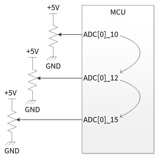
Figure 7 shows an example application that converts the voltage consecutively in the order of ADC[0]_10, ADC[0]_12 and ADC[0]_15 with one software trigger.
Ensure that you have set up the parameters as mentioned in Basic ADC global settings.
Figure 7. Example of group conversion connection
Use the information in the following sections and the example to implement this application.
Logical channel settings for group procedure
Figure 8 shows the example of logical channel setting for a group procedure in CYT2 series. In this example, the minimum value of the sample time is used. To find the proper sample time for your system, see the datasheet mentioned in Related documents.
Figure 8. Example of logical channel setting for group in CYT2 series
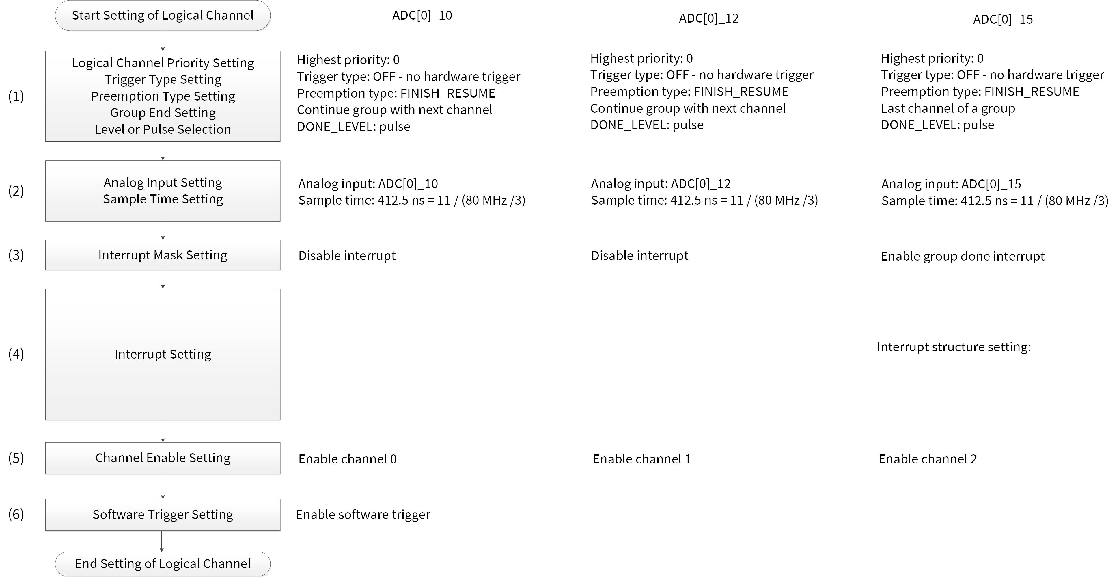
Although this example uses logical channels 0, 1, and 2, you can use any channel if those numbers are consecutive.
Use case
The following use case is an example of logical channel setting for group.
- ADC trigger selection: OFF
- Channel priority: 0 (highest)
- Channel pre-emption type: Finish resume
- Analog input, channel group and interrupt
Channel | Analog input | Channel group | Interrupt |
|---|---|---|---|
CH0 | ADC[0]_10 | Continue group with next channel | Disable |
CH1 | ADC[0]_12 | Continue group with next channel | Disable |
CH2 | ADC[0]_15 | Last channel of a group | Enable group done interrupt |
- ADC done level: Pulse
- External analog MUX: 0, Enable
- Pre-conditioning Mode: OFF
- Overlap diagnostics mode: OFF
- Calibration value select: Regular
- Post processing mode: None
- Result alignment: Right
- Sign extension: Unsigned
- Averaging count: 0
- Shift right: 0
- Mask group: Not done/Not cancelled/Not overflow
- Mask channel: Not range/Not pulse/Not overflow
Configuration
Table 11 lists the parameters and Table 12 lists the functions of logical channel setting for group in CYT2 series.
Table 11. Parameters for logical channel setting for group in CYT2
series
Parameters | Description | Value |
|---|---|---|
| ADC logical channel | 0ul |
| ADC channel number in the group | 3ul |
| First channel of ADC group | ADC_LOGICAL_CHANNEL |
| Last channel of ADC group | ADC_GROUP_FIRST_CHANNEL + ADC_GROUP_NUMBER_OF_CHANNELS - 1ul |
| Analog macro for the potentiometer on the TRAVEO™ T2G baseboard | CY_ADC_POT_MACRO: PASS0_SAR0 |
| Trigger OFF | 0ul (See Table 3) |
| Channel priority | 0ul |
| Pre-emption type | 3ul (See Table 3) |
| Is group end? | CH0: false, CH1: false, CH2: true |
| Done level | 0ul (See Table 3) |
| Pin address | BB_POTI_ANALOG_INPUT_NO |
| Port address | 0ul (See Table 3) |
| External MUX select | 0ul |
| Enable external MUX | true |
| Pre-condition mode | 0ul (See Table 3) |
| Overlap diagnostics mode | 0ul (See Table 3) |
| Sample time | samplingCycle (Calculated Value) |
| Calibration value select | 0ul (See Table 3) |
| Post processing mode | 0ul (See Table 3) |
| Result alignment | 0ul (See Table 3) |
| Sign extension | 0ul (See Table 3) |
| Average count | 0ul |
| Right shift | 0ul |
| Range detection mode | 2ul (See Table 3) |
| Range detection low threshold | 0x0000ul |
| Range detection high threshold | 0x0FFFul |
| Mask group done | CH0: false, CH1: false, CH2: true |
| Mask group cancelled | false |
| Mask group overflow | false |
| Mask channel range | false |
| Mask channel pulse | false |
| Mask channel overflow | false |
Table 12. Functions for logical channel setting for group in CYT2 series
Functions | Description | Value |
|---|---|---|
| Initializes the ADC channel | PASS SARchannel = &BB_POTI_ANALOG_MACRO->CH[ADC_LOGICAL_CHANNEL] ADCchannel Configure = adcChannelConfig |
| Initializes the referenced system interrupt by setting the interrupt vector | Config = irq_cfg |
| Enables the corresponding channel | SARchannel = PASS_SAR_CH |
| Issues a software start trigger | PASS SARchannel = &BB_POTI_ANALOG_MACRO->CH[ADC_LOGICAL_CHANNEL] |
Sample code
See Code Listing 22 for sample code for initial configuration of logical channel settings for group procedure.
Code Listing 22 Logical channel settings for group procedure
    #define BB_POTI_ANALOG_PCLK         CY_ADC_POT_PCLK
    #define BB_POTI_ANALOG_INPUT_NO    ((cy_en_adc_pin_address_t)CY_ADC_POT_IN_NO)
    :
    #define ADC_GROUP_FIRST_CHANNEL         ADC_LOGICAL_CHANNEL
    #define ADC_GROUP_LAST_CHANNEL          (ADC_GROUP_FIRST_CHANNEL + ADC_GROUP_NUMBER_OF_CHANNELS - 1u)

    uint16_t               resultBuff[ADC_GROUP_NUMBER_OF_CHANNELS][16];
    cy_stc_adc_ch_status_t statusBuff[ADC_GROUP_NUMBER_OF_CHANNELS][16];
    uint8_t                resultIdx;

    :
    int main(void)
    {
    :
        __enable_irq(); /* Enable global interrupts. */

        /* Initialize ADC */
        {
    :
            cy_stc_adc_config_t adcConfig =  /* ADC Configuration. */
            {
                .preconditionTime    = 0ul,
                .powerupTime         = 0ul,
                .enableIdlePowerDown = false,
                .msbStretchMode      = CY_ADC_MSB_STRETCH_MODE_2CYCLE,


                .enableHalfLsbConv   = 0ul,
                .sarMuxEnable        = true,
                .adcEnable           = true,
                .sarIpEnable         = true,
            };
            cy_stc_adc_channel_config_t adcChannelConfig =
            {
                .triggerSelection          = CY_ADC_TRIGGER_OFF,  /* (1) Trigger Type Setting */
                .channelPriority           = 0ul,
                .preenptionType            = CY_ADC_PREEMPTION_FINISH_RESUME,  /* Preemption Type Setting */
                .isGroupEnd                = false,  /* Group End Setting */
                .doneLevel                 = CY_ADC_DONE_LEVEL_PULSE,   /* Level or Pulse Selection  */
                .pinAddress                = BB_POTI_ANALOG_INPUT_NO,  /* (2) Analog Input Setting, Sample Time Setting */
                .portAddress               = CY_ADC_PORT_ADDRESS_SARMUX0,  /* (2) Analog Input Setting, Sample Time Setting */
                .extMuxSelect              = 0ul,  /* (2) Analog Input Setting, Sample Time Setting */
                .extMuxEnable              = true,  /* (2) Analog Input Setting, Sample Time Setting */
                .preconditionMode          = CY_ADC_PRECONDITION_MODE_OFF,  /* (2) Analog Input Setting, Sample Time Setting */
                .overlapDiagMode           = CY_ADC_OVERLAP_DIAG_MODE_OFF,  /* (2) Analog Input Setting, Sample Time Setting */
                .sampleTime                = samplingCycle,  /* (2) Analog Input Setting, Sample Time Setting */
                .calibrationValueSelect    = CY_ADC_CALIBRATION_VALUE_REGULAR,  /* (2) Analog Input Setting, Sample Time Setting */
                .postProcessingMode        = CY_ADC_POST_PROCESSING_MODE_NONE,  /* (2) Analog Input Setting, Sample Time Setting */
                .resultAlignment           = CY_ADC_RESULT_ALIGNMENT_RIGHT,  /* (2) Analog Input Setting, Sample Time Setting */
                .signExtention             = CY_ADC_SIGN_EXTENTION_UNSIGNED,  /* (2) Analog Input Setting, Sample Time Setting */
                .averageCount              = 0u,  /* (2) Analog Input Setting, Sample Time Setting */
                .rightShift                = 0u,  /* (2) Analog Input Setting, Sample Time Setting */
                .rangeDetectionMode        = CY_ADC_RANGE_DETECTION_MODE_INSIDE_RANGE,  /* (2) Analog Input Setting, Sample Time Setting */
                .rangeDetectionLoThreshold = 0x0000ul,  /* (2) Analog Input Setting, Sample Time Setting */
                .rangeDetectionHiThreshold = 0x0FFFul,  /* (2) Analog Input Setting, Sample Time Setting */


                .mask.grpDone              = false,  /* (3) Interrupt Mask Setting */
                .mask.grpCancelled         = false,  /* (3) Interrupt Mask Setting */
                .mask.grpOverflow          = false,  /* (3) Interrupt Mask Setting */
                .mask.chRange              = false,  /* (3) Interrupt Mask Setting */
                .mask.chPulse              = false,  /* (3) Interrupt Mask Setting */
                .mask.chOverflow           = false,  /* (3) Interrupt Mask Setting */
            };

            Cy_Adc_Init(BB_POTI_ANALOG_MACRO, &adcConfig);  /* ADC Configuration setting. See Code Listing 2. */


            adcChannelConfig.isGroupEnd   = false;
            adcChannelConfig.mask.grpDone = false;
            for (uint8_t ch = ADC_GROUP_FIRST_CHANNEL; ch < (ADC_GROUP_FIRST_CHANNEL + ADC_GROUP_NUMBER_OF_CHANNELS); ch++)
            {
                uint8_t i = ch - ADC_GROUP_FIRST_CHANNEL; // i is 0-based for array indexing

                if(ch == ADC_GROUP_LAST_CHANNEL)
                {
                    adcChannelConfig.isGroupEnd   = true;
                    adcChannelConfig.mask.grpDone = true;
                }
                adcChannelConfig.pinAddress = aenAnalogInput[i];


                Cy_Adc_Channel_Init(&BB_POTI_ANALOG_MACRO->CH[ch], &adcChannelConfig);  /* ADC Channel Initialize. See Code Listing 5. */
            }
    :
            Cy_SysInt_InitIRQ(&irq_cfg);  /* (4) Initialize Interrupt Request. See Code Listing 7. */
    :
        /* Enable ADC ch. */
        for (uint8_t ch = ADC_GROUP_FIRST_CHANNEL; ch < (ADC_GROUP_FIRST_CHANNEL + ADC_GROUP_NUMBER_OF_CHANNELS); ch++)
        {
            Cy_Adc_Channel_Enable(&CY_ADC_POT_MACRO->CH[ch]);  /* (5) Enable ADC Channel. See Code Listing 8. */
        }
    :


        /* Issue SW trigger */
        Cy_Adc_Channel_SoftwareTrigger(&CY_ADC_POT_MACRO->CH[ADC_GROUP_FIRST_CHANNEL]);  /* (6) Software Trigger Setting. See Code Listing 9. */
    :
        for(;;)
        {
        }
    }
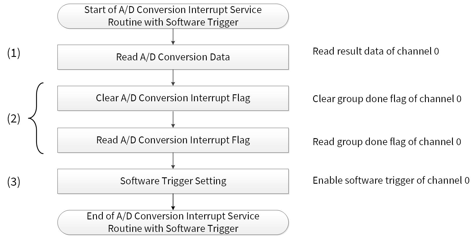
A/D conversion ISR for group
Figure 9 shows the example of ADC ISR for the group. For details on CPU interrupt handling, see the architecture TRM mentioned in the Related documents.
Figure 9. Example of ADC ISR for group
Use case
See Section 4.1.1.
Configuration
Table 13 lists the parameters and Table 14 lists the functions of the configuration part of in SDL for ADC ISR for group settings.
Table 13. Parameters for ADC ISR for group settings
Parameters | Description | Value |
|---|---|---|
| Conversion result buffer | - (Calculated Value) |
| Status result buffer | - (Calculated Value) |
| Index result | - (Calculated Value) |
| Interrupt source | - (Calculated Value) |
Table 14. Functions for ADC ISR for group settings
Functions | Description | Value |
|---|---|---|
| Gets conversion result and status | SAR Channel = BB_POTI_ANALOG_MACRO->CH[ADC_LOGICAL_CHANNEL], Result = resultBuff[resultIdx], Status = statusBuff[resultIdx] |
| Clears the corresponding channel interrupt status | SAR Channel = BB_POTI_ANALOG_MACRO->CH[ADC_LOGICAL_CHANNEL], Source = intrSource |
| Issues a software start trigger | SAR Channel = BB_POTI_ANALOG_MACRO->CH[ADC_LOGICAL_CHANNEL] |
Sample code
See Code Listing 23 for sample code for initial configuration of ADC ISR for group settings.
Code Listing 23 ADC ISR for group settings
#define BB_POTI_ANALOG_MACRO        CY_ADC_POT_MACRO
:
#define ADC_GROUP_FIRST_CHANNEL         ADC_LOGICAL_CHANNEL
#define ADC_GROUP_LAST_CHANNEL          (ADC_GROUP_FIRST_CHANNEL + ADC_GROUP_NUMBER_OF_CHANNELS - 1u)

uint16_t               resultBuff[ADC_GROUP_NUMBER_OF_CHANNELS][16];
cy_stc_adc_ch_status_t statusBuff[ADC_GROUP_NUMBER_OF_CHANNELS][16];
uint8_t                resultIdx;

void AdcIntHandler(void)
{
    cy_stc_adc_interrupt_source_t intrSource = { false };
:
    {
:
        /* Get the result(s) */
        for(uint8_t ch = ADC_GROUP_FIRST_CHANNEL; ch < (ADC_GROUP_FIRST_CHANNEL + ADC_GROUP_NUMBER_OF_CHANNELS); ch++)
        {
            uint8_t i = ch - ADC_GROUP_FIRST_CHANNEL; // i is 0-based for array indexing
            Cy_Adc_Channel_GetResult(&BB_POTI_ANALOG_MACRO->CH[ch], &resultBuff[i][resultIdx], &statusBuff[i][resultIdx]);  /* (1) Read A/D conversion data. See Code Listing 11. */
            printf("AN%d = %04d, ", aenAnalogInput[i], resultBuff[i][resultIdx]);
        }

        /* Increment result idx */
        resultIdx = (resultIdx + 1ul) % (sizeof(resultBuff[0]) / sizeof(resultBuff[0][0]));

        /* Clear interrupt source(s) (Only last channel is required) */
        Cy_Adc_Channel_ClearInterruptStatus(&BB_POTI_ANALOG_MACRO->CH[ADC_GROUP_LAST_CHANNEL], &intrSource);  /* (2) Clear and read A/D conversion flag. See Code Listing 12. */


        /* Trigger next conversion */
        Cy_Adc_Channel_SoftwareTrigger(&BB_POTI_ANALOG_MACRO->CH[ADC_GROUP_FIRST_CHANNEL]);  /* (3) Software Trigger Setting. See Code Listing 9. */
    }
    else
    {
        // Unexpected interrupt
        CY_ASSERT(false);
    }
}
Averaging procedure
Averaging is fully configured per channel by SARn_CHx_POST_CTL register.
The number of samples averaged is up to 256.
This section shows an example application that converts voltage values given to the ADC[0]_0 at the MCU to digital averaging values.
The physical setting of this application is the same as shown in Figure 1.
Ensure that you have configured the settings as described in the Basic ADC global settings, Use case, and A/D conversion ISR with software trigger sections.
Use the information in the following sections and the example to implement this application.
Averaging settings
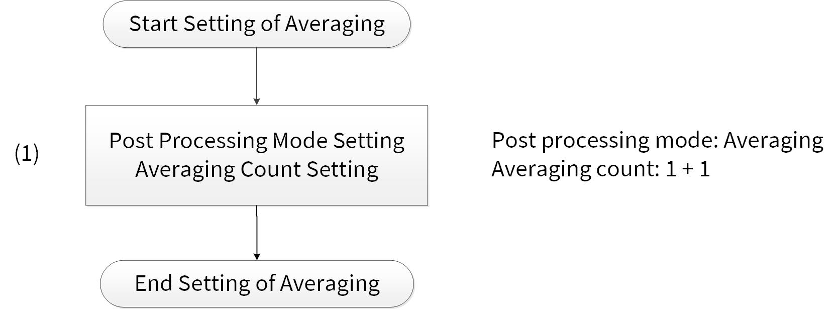
Figure 10 shows the example of averaging setting. The ADC result of the specified averaging count is accumulated, and it is shifted to the right by specifying right shift bit. Then, it is stored in the result register. For true averaging, the averaging count should be a power of 2 and the right shift should be set to the corresponding value. For an averaging count that is not a power of 2, the right shift can only approximate the required divide. In this case, if a true averaging result is required, the software will need to do a divide.
Figure 10. Example of averaging setting
Use case
The following use case is an example of averaging setting.
- Post processing mode: Averaging
- Averaging count: 1 + 1 times
- Right shift: 1
- Other use case items are the same as Section 2.3.1.
Configuration
Table 15 lists the parameters and Table 16 lists the functions of the configuration part of in SDL for averaging settings.
Table 15. Parameters for averaging
Parameters | Description | Value |
|---|---|---|
| Analog macro for the potentiometer on TRAVEO™ T2G baseboard | CY_ADC_POT_MACRO: PASS0_SAR0 |
| Trigger OFF | 0ul (See Table 3) |
| Channel priority | 0ul |
| Pre-emption type | 3ul (See Table 3) |
| Is group end? | true |
| Done level | 0ul (See Table 3) |
| Pin address | BB_POTI_ANALOG_INPUT_NO |
| Port address | 0ul (See Table 3) |
| External MUX select | 0ul |
| Enables external MUX | true |
| Pre-condition mode | 0ul (See Table 3) |
| Overlap diagnostics mode | 0ul (See Table 3) |
| Sample time | 0ul |
| Calibration value select | 0ul (See Table 3) |
| Post processing mode | 1ul (See Table 3) |
| Result alignment | 0ul (See Table 3) |
| Sign extension | 0ul (See Table 3) |
| Average count | 1ul |
| Right shift | 1ul |
| Range detection mode | 0ul (See Table 3) |
| Range detection low threshold | 0x0000ul |
| Range detection high threshold | 0x0FFFul |
| Mask group done | true |
| Mask group cancelled | false |
| Mask group overflow | false |
| Mask channel range | false |
| Mask channel pulse | false |
| Mask channel overflow | false |
Table 16. Functions for averaging
Functions | Description | Value |
|---|---|---|
| Initializes the ADC channel | PASS SARchannel = &BB_POTI_ANALOG_MACRO->CH[ADC_LOGICAL_CHANNEL] ADCchannel Configure = adcChannelConfig |
Sample code
See Code Listing 24 for sample code for initial configuration of averaging settings.
Code Listing 24 Average settings
 :
 /* ADC Channel Configuration */
 cy_stc_adc_channel_config_t adcChannelConfig =
 {
     .triggerSelection          = CY_ADC_TRIGGER_OFF,
     .channelPriority           = 0ul,
     .preenptionType            = CY_ADC_PREEMPTION_FINISH_RESUME,
     .isGroupEnd                = true,
     .doneLevel                 = CY_ADC_DONE_LEVEL_PULSE,
     .pinAddress                = BB_POTI_ANALOG_INPUT_NO,
     .portAddress               = CY_ADC_PORT_ADDRESS_SARMUX0,
     .extMuxSelect              = 0ul,
     .extMuxEnable              = true,
     .preconditionMode          = CY_ADC_PRECONDITION_MODE_OFF,
     .overlapDiagMode           = CY_ADC_OVERLAP_DIAG_MODE_OFF,
     .sampleTime                = 0ul,
     .calibrationValueSelect    = CY_ADC_CALIBRATION_VALUE_REGULAR,
     .postProcessingMode        = CY_ADC_POST_PROCESSING_MODE_AVG, /* Averaging setting */
     .resultAlignment           = CY_ADC_RESULT_ALIGNMENT_RIGHT,
     .signExtention             = CY_ADC_SIGN_EXTENTION_UNSIGNED,
     .averageCount              = 1ul, /* 1+1 times*/  /* (1) Averaging Settings */
     .rightShift                = 1ul,
     .rangeDetectionMode        = CY_ADC_RANGE_DETECTION_MODE_BELOW_LO,
     .rangeDetectionLoThreshold = 0x0000ul,
     .rangeDetectionHiThreshold = 0x0FFFul,
     .mask.grpDone              = true,
     .mask.grpCancelled         = false,
     .mask.grpOverflow          = false,
     .mask.chRange              = false,
     .mask.chPulse              = false,
     .mask.chOverflow           = false,
 };
 :
 int main(void)
 {
     /* Enable global interrupts. */
     __enable_irq();

     SystemInit();

     Cy_Adc_Channel_Init(&BB_POTI_ANALOG_MACRO->CH[ADC_LOGICAL_CHANNEL], &adcChannelConfig);  /* ADC Channel Initialize. See Code Listing 5. */
 :
     for(;;);
 }
Range detection procedure
The range detection enables a check with a high and low threshold register without CPU involvement.
Each logical channel can be enabled for range detection individually. This function is usually used to monitor abnormal values in the voltage.
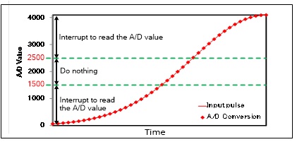
This section shows an example application that converts voltage values given to the ADC[0]_0 of the MCU to digital values. If the digital value is greater than or equal to ‘2500’ or less than ‘1500’, it generates an interrupt to read the value as shown in Figure 11. Analog-to-digital conversion is repeated at regular timing by hardware trigger of a corresponding TCPWM.
The physical setting of this application is the same as shown in Figure 1.
Ensure that you have configured the settings as described in the Basic ADC global settings and Logical channel setting with hardware trigger sections.
Figure 11. Example behavior of range detection application
Use the information in the following sections and the example to implement this application.
Range detection settings
Figure 12 shows the example of range detection setting.
Figure 12. Example of range detection setting

Use case
The following use case is an example of averaging setting.
- Range detection threshold: Low: 1500 / High: 2500
- Other use case items are the same as in Section 2.2.1 and Section 3.1.1.
Configuration
Table 17 lists the parameters and Table 18 lists the functions of the configuration part of in SDL for range detection settings.
Table 17. Parameters for range detection settings
Parameters | Description | Value |
|---|---|---|
| Analog macro for the potentiometer on the TRAVEO™ T2G baseboard | CY_ADC_POT_MACRO: PASS0_SAR0 |
| Analog input number for the potentiometer on the TRAVEO™ T2G baseboard | CH0 (CH[ADC_LOGICAL_CHANNEL]) |
| Trigger OFF | 0ul (See Table 3) |
| Channel priority | 0ul |
| Pre-emption type | 3ul (See Table 3) |
| Is group end? | true |
| Done level | 0ul (See Table 3) |
| Pin address | BB_POTI_ANALOG_INPUT_NO |
| Port address | 0ul (See Table 3) |
| External MUX select | 0ul |
| Enables external MUX | true |
| Pre-condition mode | 0ul (See Table 3) |
| Overlap diagnostics mode | 0ul (See Table 3) |
| Sample time | 0ul |
| Calibration value select | 0ul (See Table 3) |
| Post processing mode | 3ul (See Table 3) |
| Result alignment | 0ul (See Table 3) |
| Sign extension | 0ul (See Table 3) |
| Average count | 0ul |
| Right shift | 0ul |
| Range detection mode | 3ul (See Table 3) |
| Range detection low threshold | 0x09C4ul |
| Range detection high threshold | 0x05DCul |
| Mask group done | false |
| Mask group cancelled | false |
| Mask group overflow | false |
| Mask channel range | true |
| Mask channel pulse | false |
| Mask channel overflow | false |
Table 18. Functions for range detection settings
Functions | Description | Value |
|---|---|---|
| Initializes the ADC channel | PASS SARchannel = &BB_POTI_ANALOG_MACRO->CH[ADC_LOGICAL_CHANNEL] ADCchannel Configure = adcChannelConfig |
| Initializes the referenced system interrupt by setting the interrupt vector | Config = irq_cfg |
| Enables the corresponding channel | PASS SARchannel = &BB_POTI_ANALOG_MACRO->CH[ADC_LOGICAL_CHANNEL] |
| Issues a software start trigger | PASS SARchannel = &BB_POTI_ANALOG_MACRO->CH[ADC_LOGICAL_CHANNEL] |
Sample code
See Code Listing 25 for sample code for initial configuration of range detection settings.
Code Listing 25 Range detection settings
    :
    #define BB_POTI_ANALOG_INPUT_NO    ((cy_en_adc_pin_address_t)CY_ADC_POT_IN_NO)
     :
    /* ADC Channel Configuration */
    cy_stc_adc_channel_config_t adcChannelConfig =
    {
        .triggerSelection          = CY_ADC_TRIGGER_GENERIC0,
        .channelPriority           = 0ul,
        .preenptionType            = CY_ADC_PREEMPTION_FINISH_RESUME,
        .isGroupEnd                = true,
        .doneLevel                 = CY_ADC_DONE_LEVEL_PULSE,
        .pinAddress                = BB_POTI_ANALOG_INPUT_NO,
        .portAddress               = CY_ADC_PORT_ADDRESS_SARMUX0,
        .extMuxSelect              = 0ul,
        .extMuxEnable              = true,
        .preconditionMode          = CY_ADC_PRECONDITION_MODE_OFF,
        .overlapDiagMode           = CY_ADC_OVERLAP_DIAG_MODE_OFF,
        .sampleTime                = 0ul, /* It will be update */
        .calibrationValueSelect    = CY_ADC_CALIBRATION_VALUE_REGULAR,
        .postProcessingMode        = CY_ADC_POST_PROCESSING_MODE_RANGE, /* Range detection */  /* (1) Post Processing Mode Setting. */
        .resultAlignment           = CY_ADC_RESULT_ALIGNMENT_RIGHT,
        .signExtention             = CY_ADC_SIGN_EXTENTION_UNSIGNED,
        .averageCount              = 0ul,
        .rightShift                = 0ul,
        .rangeDetectionMode        = CY_ADC_RANGE_DETECTION_MODE_OUTSIDE_RANGE,/* Outside Mode */
        .rangeDetectionLoThreshold = 0x09C4ul, /* 2500 */  /* (2) Range Detection Value Setting. */
        .rangeDetectionHiThreshold = 0x05DCul, /* 1500 */
        .mask.grpDone              = false,
        .mask.grpCancelled         = false,
        .mask.grpOverflow          = false,
        .mask.chRange              = true, /* Range detection interrupt */  /* (3) Range Detection Interrupt Setting. */
        .mask.chPulse              = false,
        .mask.chOverflow           = false,
    };
    :
    int main(void)
    {
        __enable_irq(); /* Enable global interrupts. */

        SystemInit();
     :
        /* Initialize ADC */  /* Initialize ADC Channel. See Code Listing 5. */
        uint32_t samplingCycle = (uint32_t)DIV_ROUND_UP((ANALOG_IN_SAMPLING_TIME_MIN_IN_NS * (uint64_t)actualAdcOperationFreq), 1000000000ull);
        adcChannelConfig.sampleTime = samplingCycle;
     :
        Cy_Adc_Channel_Init(&BB_POTI_ANALOG_MACRO->CH[ADC_LOGICAL_CHANNEL], &adcChannelConfig);
     :
        /* Register ADC interrupt handler and enable interrupt */
        cy_stc_sysint_irq_t irq_cfg;
        irq_cfg = (cy_stc_sysint_irq_t){
                .sysIntSrc  = (cy_en_intr_t)((uint32_t)CY_ADC_POT_IRQN + ADC_LOGICAL_CHANNEL),
                .intIdx     = CPUIntIdx3_IRQn,
                .isEnabled  = true,
        };
        Cy_SysInt_InitIRQ(&irq_cfg);  /* Initialize Interrupt Request. See Code Listing 7. */

     :

        /* Enable ADC ch. */  /* Enable ADC Channel. See Code Listing 8. */
        Cy_Adc_Channel_Enable(&BB_POTI_ANALOG_MACRO->CH[ADC_LOGICAL_CHANNEL]);
        /* Issue SW trigger */
        Cy_Adc_Channel_SoftwareTrigger(&BB_POTI_ANALOG_MACRO->CH[ADC_LOGICAL_CHANNEL]);  /* Software Trigger Setting. See Code Listing 9. */

    :

        for(;;);
    }
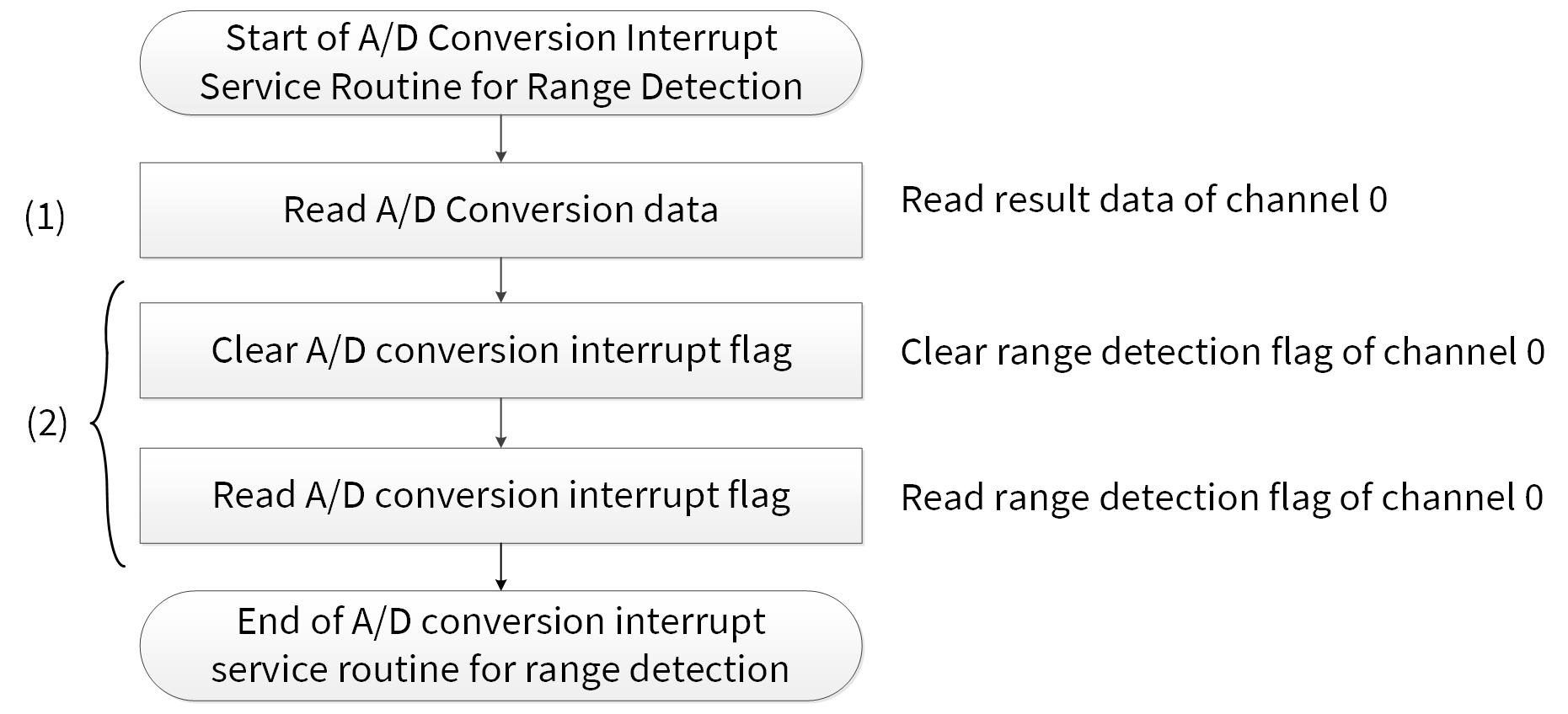
A/D conversion ISR for range detection
Figure 13 shows the example of ADC ISR for a range detection. For details on CPU interrupt handing, see the architecture TRM mentioned in Related documents.
Figure 13. Example of ADC ISR for range detection
Configuration
Table 19 lists the parameters and Table 20 lists the functions of the configuration part of in SDL for ADC ISR for range detection settings.
Table 19. Parameters for ADC ISR for range detection settings
Parameters | Description | Value |
|---|---|---|
| Analog macro for the potentiometer on the TRAVEO™ T2G baseboard | CY_ADC_POT_MACRO: PASS0_SAR0 |
| Interrupt source | - (Calculated Value) |
| Index result | - (Calculated Value) |
Table 20. Functions for ADC ISR for range detection settings
Functions | Description | Value |
|---|---|---|
| Returns the interrupt status | PASS SARchannel = &BB_POTI_ANALOG_MACRO->CH[ADC_LOGICAL_CHANNEL] INTR Source = &intrSource |
| Gets the conversion result and status | SAR Channel = BB_POTI_ANALOG_MACRO->CH[ADC_LOGICAL_CHANNEL], Result = resultBuff[resultIdx], Status = statusBuff[resultIdx] |
| Clears the corresponding channel interrupt status | SAR Channel = BB_POTI_ANALOG_MACRO->CH[ADC_LOGICAL_CHANNEL], Source = intrSource |
Sample code
See Code Listing 26 for sample code for initial configuration of ADC ISR for range detection settings.
Code Listing 26 ADC ISR for range detection settings
    :
    /* ADC Interrupt Hanlder */
    void AdcIntHandler(void)
    {
        cy_stc_adc_interrupt_source_t intrSource = { false };


        /* Get interrupt source */  /* Get Interrupt Masked Status. See Code Listing 14. */
        Cy_Adc_Channel_GetInterruptMaskedStatus(&BB_POTI_ANALOG_MACRO->CH[ADC_LOGICAL_CHANNEL], &intrSource);

        if(intrSource.chRange)
        {
            /* Get the result(s) */  /* (1) Read A/D conversion data. See Code Listing 11. */
            Cy_Adc_Channel_GetResult(&BB_POTI_ANALOG_MACRO->CH[ADC_LOGICAL_CHANNEL], &resultBuff[resultIdx], &statusBuff[resultIdx]);

            /* Increment result idx */
            resultIdx = (resultIdx + 1) % (sizeof(resultBuff) / sizeof(resultBuff[0]));


            /* Clear interrupt source */  /* (2) Clear and read A/D conversion flag. See Code Listing 12. */
            Cy_Adc_Channel_ClearInterruptStatus(&BB_POTI_ANALOG_MACRO->CH[ADC_LOGICAL_CHANNEL], &intrSource);

        }
        else
        {
            /* Unexpected interrupt */
            CY_ASSERT(false);
        }
    }
    :
Pulse detection procedure
The result of comparison from range detection can be filtered with the pulse detection function.
For every logical channel, the pulse detection function has a pair of reload registers to store the initial value for the positive and negative down counters. The positive and negative counters decrement on positive and negative events obtained from the result of the comparison done by the range detection.
This function is usually used to avoid misdetections of abnormal voltage caused by noise and so on when monitoring voltage.
For parameters described in the Range detection settings, an analog-to-digital conversion result greater than or equal to 2500 or lesser than 1500 is a positive event; one greater than or equal to 1500 and lesser than 2500 is a negative event.
This example application generates an interrupt if the positive event has occurred five times in a row as shown in Figure 14.
The continuous number of positive events is cancelled when a negative event occurs twice in a row; that is, the count of positive event continues even if negative event has occurred just once as shown in Figure 15.
The physical setting of this application is the same as shown in Figure 1.
Ensure that you have configured the settings described in the Basic ADC global settings and Logical channel setting with hardware trigger sections.
Figure 14. Example behavior of pulse detection application 1Example behavior
of pulse detection application 2
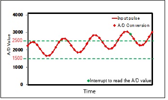
Figure 15. Example behavior of pulse detection application 2
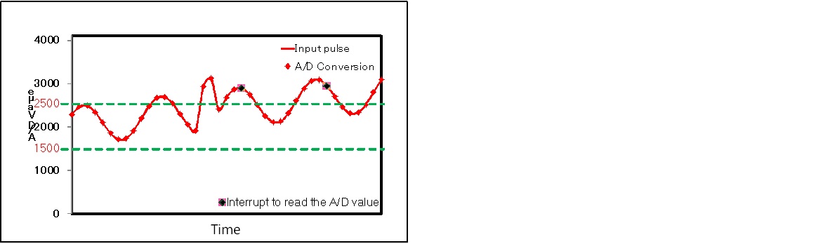
Use the information in the following sections and the example to implement this application.
Pulse detection settings
Figure 16 shows an example of pulse detection setting.
Figure 16. Example of pulse detection setting
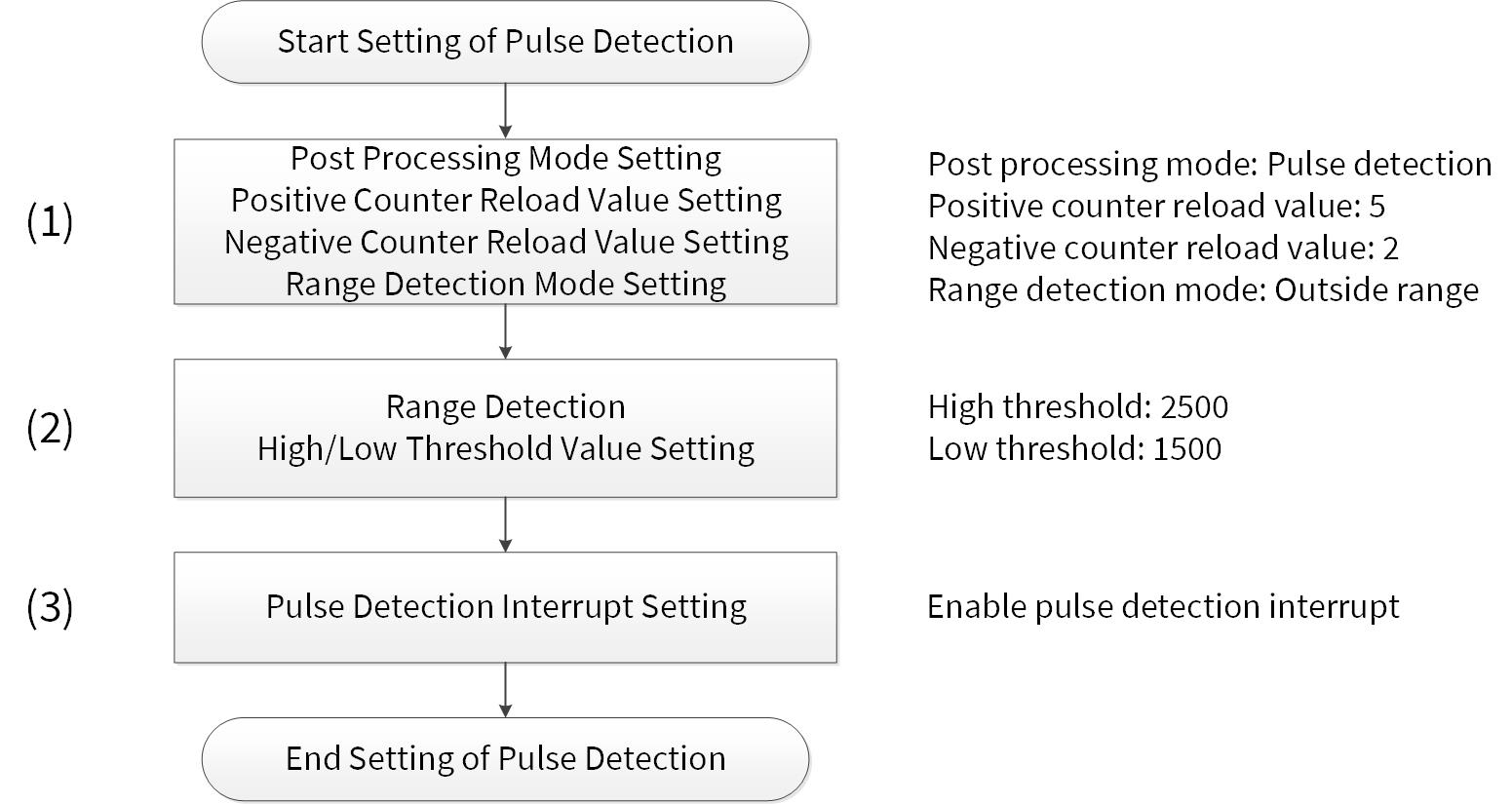
Use case
The following use case is an example of pulse detection settings.
- Analog input: ADC[0]_0
- Range detection threshold: Low: 1500 / High: 2500
- ADC trigger: TCPWM
- Positive counter reload value: 5
- Negative counter reload value: 2
Other use case items are the same as Section 2.2.1 and Section 3.1.1.
Configuration
Table 21 lists the parameters and Table 22 lists the functions of the configuration part of in SDL for pulse detection settings.
Table 21. Parameters for pulse detection settings
Parameters | Description | Value |
|---|---|---|
| Analog macro for the potentiometer on the TRAVEO™ T2G baseboard | CY_ADC_POT_MACRO: PASS0_SAR0 |
| Analog input number for the potentiometer on the TRAVEO™ T2G baseboard | CH0 (CH[ADC_LOGICAL_CHANNEL]) |
| Trigger TCPWM | 1ul (See Table 3) |
| Channel priority | 0ul |
| Pre-emption type | 3ul (See Table 3) |
| Is group end? | true |
| Done level | 0ul (See Table 3) |
| Pin address | BB_POTI_ANALOG_INPUT_NO |
| Port address | 0ul (See Table 3) |
| External MUX select | 0ul |
| Enables external MUX | true |
| Pre-condition mode | 0ul (See Table 3) |
| Overlap diagnostics mode | 0ul (See Table 3) |
| Sample time | 0ul |
| Calibration value select | 0ul (See Table 3) |
| Post processing mode | 4ul (See Table 3) |
| Result alignment | 0ul (See Table 3) |
| Sign extension | 0ul (See Table 3) |
| Average count is the positive counter reload value in pulse detection mode | 5ul |
| Right shift is the negative counter reload value in pulse detection mode | 2ul |
| Range detection mode | 3ul (See Table 3) |
| Range detection low threshold | 0x05DCul |
| Range detection high threshold | 0x09C4ul |
| Mask group done | false |
| Mask group cancelled | false |
| Mask group overflow | false |
| Mask channel range | false |
| Mask channel pulse | true |
| Mask channel overflow | false |
Table 22. Functions for pulse detection settings
Functions | Description | Value |
|---|---|---|
| Initializes the ADC channel | PASS SARchannel = &BB_POTI_ANALOG_MACRO->CH[ADC_LOGICAL_CHANNEL] ADCchannel Configure = adcChannelConfig |
| Initializes the referenced system interrupt by setting the interrupt vector | Config = irq_cfg |
| Enables the corresponding channel | PASS SARchannel = &BB_POTI_ANALOG_MACRO->CH[ADC_LOGICAL_CHANNEL] |
| De-initializes the TCPWM block | Group Counter = TCPWMx_GRPx_CNTx_PWM |
| Triggers a software start on the selected TCPWMs | Group Counter = TCPWMx_GRPx_CNTx_PWM |
Sample code
See Code Listing 27.
Code Listing 27 Pulse detection settings
     :
    #define BB_POTI_ANALOG_INPUT_NO     0
    :
    /* ADC Configuration */
    :
    cy_stc_adc_channel_config_t adcChannelConfig =
    {
        .triggerSelection          = CY_ADC_TRIGGER_TCPWM,
        .channelPriority           = 0ul,
        .preenptionType            = CY_ADC_PREEMPTION_FINISH_RESUME,
        .isGroupEnd                = true,
        .doneLevel                 = CY_ADC_DONE_LEVEL_PULSE,
        .pinAddress                = BB_POTI_ANALOG_INPUT_NO,
        .portAddress               = CY_ADC_PORT_ADDRESS_SARMUX0,
        .extMuxSelect              = 0ul,
        .extMuxEnable              = true,
        .preconditionMode          = CY_ADC_PRECONDITION_MODE_OFF,
        .overlapDiagMode           = CY_ADC_OVERLAP_DIAG_MODE_OFF,
        .sampleTime                = 0ul,
        .calibrationValueSelect    = CY_ADC_CALIBRATION_VALUE_REGULAR,
        .postProcessingMode        = CY_ADC_POST_PROCESSING_MODE_RANGE_PULSE, /* Pulse Mode setting */  /* (1) Post Processing Mode Setting. */
        .resultAlignment           = CY_ADC_RESULT_ALIGNMENT_RIGHT,
        .signExtention             = CY_ADC_SIGN_EXTENTION_UNSIGNED,
        .averageCount              = 5ul, /* Positive counter reload value */
        .rightShift                = 2ul, /* Negative counter reload value */
        .rangeDetectionMode        = CY_ADC_RANGE_DETECTION_MODE_OUTSIDE_RANGE, /* Outside Mode */
        .rangeDetectionLoThreshold = 0x05DCul, /* 1500 */  /* (2) Range Detection Value Setting.*/
        .rangeDetectionHiThreshold = 0x09C4ul, /* 2500 */
        .mask.grpDone              = false,
        .mask.grpCancelled         = false,
        .mask.grpOverflow          = false,
        .mask.chRange              = false,
        .mask.chPulse              = true, /* Enable pulse detection interrupt */  /* (3) Pulse Detection Interrupt Setting. */
        .mask.chOverflow           = false,
    };
    :
    int main(void)
    {
        __enable_irq(); /* Enable global interrupts. */

        SystemInit();
    :
        /* Initialize ADC */
        uint32_t samplingCycle = (uint32_t)DIV_ROUND_UP((ANALOG_IN_SAMPLING_TIME_MIN_IN_NS * (uint64_t)actualAdcOperationFreq), 1000000000ull);
        adcChannelConfig.sampleTime = samplingCycle;

    :

        Cy_Adc_Channel_Init(&BB_POTI_ANALOG_MACRO->CH[ADC_LOGICAL_CHANNEL], &adcChannelConfig);  /* ADC Channel Initialize. See Code Listing 5. */

        /* Register ADC interrupt handler and enable interrupt */
        cy_stc_sysint_irq_t irq_cfg;
        irq_cfg = (cy_stc_sysint_irq_t){
                .sysIntSrc  = pass_0_interrupts_sar_0_IRQn,
                .intIdx     = CPUIntIdx3_IRQn,
                .isEnabled  = true,
            };


        Cy_SysInt_InitIRQ(&irq_cfg);  /* Initialize Interrupt Request. See Code Listing 7. */
    :
        /* Clock Configuration for TCPWMs */
        uint32_t sourceFreq = 80000000ul;
        uint32_t targetFreq = 2000000ul;
        uint32_t divNum_PWM = (sourceFreq / targetFreq);
        CY_ASSERT((sourceFreq % targetFreq) == 0ul); // target frequency accuracy

    :

        /* Enable ADC ch. and PWM */
        Cy_Adc_Channel_Enable(&BB_POTI_ANALOG_MACRO->CH[ADC_LOGICAL_CHANNEL]);   /* Enable ADC Channel. See Code Listing 8. */
        Cy_Tcpwm_Pwm_Enable(TCPWMx_GRPx_CNTx_PWM);  /* TCPWM PWM Enable. See Code Listing 18. */
        Cy_Tcpwm_TriggerStart(TCPWMx_GRPx_CNTx_PWM);  /* TCPWM Trigger Start Select. See Code Listing 19. */

    :

        for(;;);
    }
A/D conversion ISR for pulse detection
Figure 17 shows the example of ADC ISR for a pulse detection. For details on CPU interrupt handling, see the architecture technical reference manual mentioned in Related documents.
Figure 17. Example of ADC ISR for pulse detection

Configuration
Table 23 lists the parameters and Table 24 lists the functions of the configuration part of in SDL for ADC global settings.
Table 23. Parameters for ADC ISR for pulse detection settings
Parameters | Description | Value |
|---|---|---|
| Analog macro for the potentiometer on the TRAVEO™ T2G baseboard | CY_ADC_POT_MACRO: PASS0_SAR0 |
| Interrupt source | - (Calculated Value) |
| Index result | - (Calculated Value) |
Table 24. List of ADC ISR for pulse detection settings functions
Functions | Description | Value |
|---|---|---|
| Returns the interrupt status | PASS SARchannel = &BB_POTI_ANALOG_MACRO->CH[ADC_LOGICAL_CHANNEL] INTR Source = &intrSource |
| Clears the corresponding channel interrupt status | SAR Channel = BB_POTI_ANALOG_MACRO->CH[ADC_LOGICAL_CHANNEL], Source = intrSource |
Sample code
See Code Listing 28 for initial configuration of ADC ISR for pulse detection settings.
Code Listing 28 ADC ISR for pulse detection settings
    :
    /* ADC Interrupt Hanlder */
    void AdcIntHandler(void)
    {
        cy_stc_adc_interrupt_source_t intrSource = { false };


        /* Get interrupt source */
        Cy_Adc_Channel_GetInterruptMaskedStatus(&BB_POTI_ANALOG_MACRO->CH[ADC_LOGICAL_CHANNEL], &intrSource);  /* Get Interrupt Masked Status. See Code Listing 14. */

        if(intrSource.chPulse)
        {
    :
            /* Clear interrupt source */
            Cy_Adc_Channel_ClearInterruptStatus(&BB_POTI_ANALOG_MACRO->CH[ADC_LOGICAL_CHANNEL], &intrSource);  */ (1    ) Clear and read A/D conversion flag. See Code Listing 12. */
        }
        else
        {

            CY_ASSERT(false);
        }
    }
Diagnosis using reference voltages
This section shows flowcharts and examples that check if the A/D value is stuck while using the reference voltages.
It is possible to input from the ADC to reference voltages VREFH and VREFL, as shown in Figure 18.
VREFH is the upper-limit reference voltage. The A/D value is 0xFFF (= 4095).
VREFL is the lower-limit reference voltage. The A/D value is 0x000 (= 0).
These are the functions for ADC diagnosis and ADC calibration.
Figure 18. VREFH and VREFL as analog input
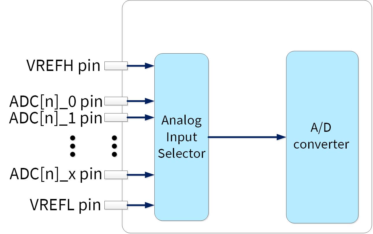
Determining the threshold
To determine the threshold for the sticking diagnosis of the A/D value, this example refers to the minimum value of the zero-transition voltage (VZT) and the maximum value of the full-scale transition voltage (VFST) in the datasheet mentioned in Related documents.
According to the datasheet, the minimum value of VZT is �–20 mV. When the analog input is 0 V, the A/D value is 16.4 (20 / (5000 / 4096)).
Therefore, when the ideal VREFL is input to the ADC, the value will be 16 or lower. (Threshold L ≤ 16 = 0x010).
The maximum value of VFST is +20 mV. When the analog input is 5 V, the A/D value is 4079.6 ((5000 – 20) / (5000 / 4096)).
Therefore, when the ideal VREFH is input to the ADC, the value will be 4080 or higher. (Threshold H ≥ 4080 = 0xFF0).
Note: These thresholds are determined in an ideal environment. However, the A/D value is affected by environmental factors, such as power supply voltage, reference voltage, input analog voltage, temperature, and noise. Therefore, when determining the final thresholds, it is recommended to add some margin considering the user system environment.
ADC sticking diagnosis procedure
Figure 19 shows the ADC sticking diagnosis flowchart. In this example, the minimum value of the sample time is used. If the temperature sensor channel is enabled, the reference buffer mode should also be enabled. To find the proper sample time for your system, see the datasheet mentioned in Related documents.
Figure 19. Example of ADC sticking diagnosis flowchart
Use case
The following use case is an example of ADC sticking diagnosis settings.
- Analog input setting:
- VREFH
- VREFL
- Sample time: 2 µs
Configuration
Table 25 lists the parameters and Table 26 lists the functions of the configuration part of in SDL for ADC sticking diagnosis settings.
Table 25. Parameters for ADC sticking diagnosis settings
Parameters | Description | Value |
|---|---|---|
adcChannelConfig.triggerSelection | Trigger OFF | 0ul (See Table 3) |
adcChannelConfig.channelPriority | Channel priority | 0ul |
adcChannelConfig.preenptionType | Pre-emption type | 3ul (See Table 3) |
adcChannelConfig.isGroupEnd | Is group end? | true |
adcChannelConfig.doneLevel | Done level | 0ul (See Table 3) |
adcChannelConfig.pinAddress | Pin address | When setting VREFH: CY_ADC_PIN_ADDRESS_VREF_H When setting VREFL: CY_ADC_PIN_ADDRESS_VREF_L |
adcChannelConfig.portAddress | Port address | 0ul (See Table 3) |
adcChannelConfig.extMuxSelect | External MUX select | 0ul |
adcChannelConfig.extMuxEnable | Enables external MUX | false |
adcChannelConfig.preconditionMode | Pre-condition mode | 0ul (See Table 3) |
adcChannelConfig.overlapDiagMode | Overlap diagnostics mode | 0ul (See Table 3) |
adcChannelConfig.sampleTime | Sample time | 0ul |
adcChannelConfig.calibrationValueSelect | Calibration value select | 0ul (See Table 3) |
adcChannelConfig.postProcessingMode | Post processing mode | 0ul (See Table 3) |
adcChannelConfig.resultAlignment | Result alignment | 0ul (See Table 3) |
adcChannelConfig.signExtention | Sign extension | 0ul (See Table 3) |
adcChannelConfig.averageCount | Average count | 0ul |
adcChannelConfig.rightShift | Right shift | 0ul |
adcChannelConfig.rangeDetectionMode | Range detection mode | 1ul (See Table 3) |
adcChannelConfig.rangeDetectionLoThreshold | Range detection low threshold | 0ul |
adcChannelConfig.rangeDetectionHiThreshold | Range detection high threshold | 0ul |
adcChannelConfig.mask.grpDone | Mask group done | false |
adcChannelConfig.mask.grpCancelled | Mask group cancelled | false |
adcChannelConfig.mask.grpOverflow | Mask group overflow | false |
adcChannelConfig.mask.chRange | Mask channel range | false |
adcChannelConfig.mask.chPulse | Mask channel pulse | false |
adcChannelConfig.mask.chOverflow | Mask channel overflow | false |
CY_ADC_REF_BUF_MODE_ON | Select reference buffer mode 0: No reference mode selected 1: Reference buffered Vbg from SRSS 3: Reference unbuffered Vbg from SRSS | 1ul |
BB_POTI_ANALOG_MACRO | Analog macro for the potentiometer on TRAVEO™ T2G baseboard | CY_ADC_POT_MACRO: PASS0_SAR0 |
Table 26. Functions for ADC sticking diagnosis settings
Functions | Description | Value |
|---|---|---|
Cy_Adc_Channel_Init(PASS SARchannel,ADCchannel Configure) | Initializes the ADC channel | PASS SARchannel = &BB_POTI_ANALOG_MACRO->CH[ADC_LOGICAL_CHANNEL] ADCchannel Configure = adcChannelConfig |
Cy_Adc_SetReferenceBufferMode(PASS0_EPASS_ MMIO,RefBufMode) | Sets the ePASS MMIO reference buffer mode | RefBufMode = CY_ADC_REF_BUF_MODE_ON |
Cy_Adc_Diag_Enable(AnalogMacro) | Enables the diagnosis function | AnalogMacro = BB_POTI_ANALOG_MACRO |
Cy_Adc_Channel_Enable(PASS SARchannel) | Enables the corresponding channel | PASS SARchannel = &BB_POTI_ANALOG_MACRO->CH[ADC_LOGICAL_CHANNEL] |
Cy_Adc_Channel_SoftwareTrigger(PASS SARchannel) | Issues a software start trigger | PASS SARchannel = &BB_POTI_ANALOG_MACRO->CH[ADC_LOGICAL_CHANNEL] |
Cy_Adc_Channel_GetGroupStatus(PASS SARchannel, GroupStatus) | Returns the group conversion status | PASS SARchannel = &BB_POTI_ANALOG_MACRO->CH[ADC_LOGICAL_CHANNEL] |
Cy_Adc_Channel_GetResult(SAR Channel,Result,Status) | Gets the conversion result and status | SAR Channel = BB_POTI_ANALOG_MACRO->CH[ADC_LOGICAL_CHANNEL], Result = resultBuff[resultIdx], Status = statusBuff[resultIdx] |
Sample code
See Code Listing 29 to Code Listing 32 for sample code for the initial configuration of ADC diagnosis settings.
Code Listing 29 ADC diagnosis settings
    :
    /* ADC logical channel to be used */
    :
    #define BB_POTI_ANALOG_PCLK         CY_ADC_POT_PCLK
    #define BB_POTI_ANALOG_INPUT_NO    ((cy_en_adc_pin_address_t)CY_ADC_POT_IN_NO)
    :
    /* ADC Channel Configuration */
    cy_stc_adc_channel_config_t adcChannelConfig =
    {
        .triggerSelection          = CY_ADC_TRIGGER_OFF,
        .channelPriority           = 0ul,
        .preenptionType            = CY_ADC_PREEMPTION_FINISH_RESUME,
        .isGroupEnd                = true,
        .doneLevel                 = CY_ADC_DONE_LEVEL_PULSE,
         /* (1) Analog Input Setting = VREFH. */
        .pinAddress                = CY_ADC_PIN_ADDRESS_VREF_H, /* Analog input setting */
        .portAddress               = CY_ADC_PORT_ADDRESS_SARMUX0,
        .extMuxSelect              = 0ul,
        .extMuxEnable              = false,
        .preconditionMode          = CY_ADC_PRECONDITION_MODE_OFF,
        .overlapDiagMode           = CY_ADC_OVERLAP_DIAG_MODE_OFF,
        .sampleTime                = 0ul,
        .calibrationValueSelect    = CY_ADC_CALIBRATION_VALUE_REGULAR,
        .postProcessingMode        = CY_ADC_POST_PROCESSING_MODE_NONE,
        .resultAlignment           = CY_ADC_RESULT_ALIGNMENT_RIGHT,
        .signExtention             = CY_ADC_SIGN_EXTENTION_UNSIGNED,
        .averageCount              = 0ul,
        .rightShift                = 0ul,
        .rangeDetectionMode        = CY_ADC_RANGE_DETECTION_MODE_INSIDE_RANGE,
        .rangeDetectionLoThreshold = 0ul,
        .rangeDetectionHiThreshold = 0ul,
        .mask.grpDone              = false,
        .mask.grpCancelled         = false,
        .mask.grpOverflow          = false,
        .mask.chRange              = false,
        .mask.chPulse              = false,
        .mask.chOverflow           = false,
    };
    :
    /* Code Example for ADC Sticking Diagnosis  */

    int main(void)
    {
        __enable_irq(); /* Enable global interrupts. */

        SystemInit();
    :
        /* Initialize ADC */
        /* 2us (2000ns) = 40/ *(80MHz/4) */
        uint32_t samplingCycle = (uint32_t)DIV_ROUND_UP((2000 * (uint64_t)actualAdcOperationFreq), 1000000000ull);
        adcChannelConfig.sampleTime = samplingCycle;

    :

    /* Initialize ADC Channel. [See Code Listing 5](#code-listing-5-cy_adc_channel_init-function) */
        Cy_Adc_Channel_Init(&BB_POTI_ANALOG_MACRO->CH[ADC_LOGICAL_CHANNEL], &adcChannelConfig);


        /* Set ePASS MMIO reference buffer mode */
        /* (2) Set REF_BUF MODE. See [Code Listing 30](#code-listing-30-cy_adc_setreferencebuffermode-function) */
        Cy_Adc_SetReferenceBufferMode(PASS0_EPASS_MMIO,CY_ADC_REF_BUF_MODE_ON);


        /* Enable diag function. */
        /* (3) Enable ADC Diagnosis. See [Code Listing 31](#code-listing-32-cy_adc_channel_getgroupstatus-function). */
        Cy_Adc_Diag_Enable(BB_POTI_ANALOG_MACRO);
        /* Enable ADC ch. */
        /* (4) Enable ADC Channel. See [Code Listing 8](#code-listing-8-cy_adc_channel_enable-function) */
        Cy_Adc_Channel_Enable(&BB_POTI_ANALOG_MACRO->CH[ADC_LOGICAL_CHANNEL]);
        /* Issue SW trigger */
        /* Software Trigger Setting. See [Code Listing 9](#code-listing-9-cy_adc_channel_softwaretrigger-function) */
        Cy_Adc_Channel_SoftwareTrigger(&BB_POTI_ANALOG_MACRO->CH[ADC_LOGICAL_CHANNEL]);


        for(;;)
        {
            status = DiagnosisProcedure();
            if(Test_Completed == 1 && status == CY_SUCCESS)
            {
                while(1);
            }
        }

    }
    cy_en_status_t DiagnosisProcedure(void)
    {
        status = CY_BAD_PARAM;

        /* Wait Group Done */
        cy_stc_adc_group_status_t Groupstatus = { false };
        do
        {
        /* Returns group conversion status. [See Code Listing 32](#code-listing-32-cy_adc_channel_getgroupstatus-function) */
        Cy_Adc_Channel_GetGroupStatus(&BB_POTI_ANALOG_MACRO->CH[ADC_LOGICAL_CHANNEL],&Groupstatus);
        }
        while(Groupstatus.grpComplete == false);

        /* Get the result(s) */
        /*Read A/D conversion data. See [Code Listing 11](#code-listing-11-cy_adc_channel_getresult-function) */
        Cy_Adc_Channel_GetResult(&BB_POTI_ANALOG_MACRO->CH[ADC_LOGICAL_CHANNEL], &resultBuff[resultIdx], &statusBuff[resultIdx]);

        /* Get the AD value */
        uint16_t AD_Value = resultBuff[resultIdx];

        /* Increment result idx */
        resultIdx = (resultIdx + 1) % (sizeof(resultBuff) / sizeof(resultBuff[0]));


        if(Flag_VREFL == 1)
        {
            /*Is the AD Value lower than threshold L */
            /* (8) Is the A/D value lower than threshold L */
            if(AD_Value <= 16) /* + 20 mV */
            {
                Flag_VREFL = 0;
    	   Test_Completed = 1;

                status = CY_SUCCESS;
                return(status);
            }
            else
            {
                /*AD Value Higher than threshold L */
                return(CY_BAD_PARAM);
            }
        }

        /* Is the A/D value Higher than threshold H */
        /* (5) Is the A/D value higher than threshold H */
        if(AD_Value >= 4080 && Flag_VREFL == 0) /*  5000 mV - 20 mV */
        {
            Flag_VREFL = 1;

            /* (6) Analog Input Setting = VREFL */
            adcChannelConfig.pinAddress = CY_ADC_PIN_ADDRESS_VREF_L;

    /* ADC Channel Initialize. See [Code Listing 5](#code-listing-5-cy_adc_channel_init-function) */
            Cy_Adc_Channel_Init(&BB_POTI_ANALOG_MACRO->CH[ADC_LOGICAL_CHANNEL], &adcChannelConfig);

            /* Enable ADC ch. */

    /* (7) Enable ADC Channel. See [Code Listing 8](#code-listing-8-cy_adc_channel_enable-function) */
            Cy_Adc_Channel_Enable(&BB_POTI_ANALOG_MACRO->CH[ADC_LOGICAL_CHANNEL]);

            /* Trigger next conversion */

    /* Software Trigger Setting. See [Code Listing 9] */
            Cy_Adc_Channel_SoftwareTrigger(&BB_POTI_ANALOG_MACRO->CH[ADC_LOGICAL_CHANNEL]);
        }
        else
        {
            /* A/D value lower than threshold H */
            return(CY_BAD_PARAM);
        }
    }
Code Listing 30 Cy_Adc_SetReferenceBufferMode() function
void Cy_Adc_SetReferenceBufferMode(volatile stc_PASS_EPASS_MMIO_t * base, cy_en_adc_ref_buf_mode_t mode)
{
    base->unPASS_CTL.stcField.u2REFBUF_MODE = mode;
}
Code Listing 31 Cy_Adc_Diag_Enable() function
void Cy_Adc_Diag_Enable(volatile stc_PASS_SAR_t * base)
{
    base->unDIAG_CTL.stcField.u1DIAG_EN = 1ul;
}
Code Listing 32 Cy_Adc_Channel_GetGroupStatus() function
 cy_en_adc_status_t Cy_Adc_Channel_GetGroupStatus(const volatile stc_PASS_SAR_CH_t * base, cy_stc_adc_group_status_t * status)
 {
      cy_en_adc_status_t ret = CY_ADC_SUCCESS;
      un_PASS_SAR_CH_GRP_STAT_t unHwStat = { 0ul };

      if (NULL != status)
      {
          unHwStat.u32Register    = base->unGRP_STAT.u32Register;
          status->chOverflow      = (unHwStat.stcField.u1CH_OVERFLOW       != 0ul) ? true : false;
          status->chPulseComplete = (unHwStat.stcField.u1CH_PULSE_COMPLETE != 0ul) ? true : false;
          status->chRangeComplete = (unHwStat.stcField.u1CH_RANGE_COMPLETE != 0ul) ? true : false;
          status->grpBusy         = (unHwStat.stcField.u1GRP_BUSY          != 0ul) ? true : false;
          status->grpCancelled    = (unHwStat.stcField.u1GRP_CANCELLED     != 0ul) ? true : false;
          status->grpComplete     = (unHwStat.stcField.u1GRP_COMPLETE      != 0ul) ? true : false;
          status->grpOverflow     = (unHwStat.stcField.u1GRP_OVERFLOW      != 0ul) ? true : false;
     }
      else
      {
          ret = CY_ADC_BAD_PARAM;
      }
      return ret;
 }
Calibration function
It is possible to adjust the offset and gain of the ADC using the SARn_ANA_CAL register.
This section describes the effects of this register and how to process the calibration of the ADC.
Offset adjustment direction
The ADC has an offset adjustment function to compensate for offset error.
The SARn_ANA_CAL[7:0] register can adjust the offset.
It is possible to select code from +127 to –128 in a decimal number for SARn_ANA_CAL[7:0].
The offset adjustment step is a quarter of 1LSb.
The equation follows (OFST = the value of SARn_ANA_CAL[7:0]):
O u t p u t D i g i t a l C o d e = m a x 0 , min 4095 , f l o o r V I N V R E F H × 4096 + O F S T 4
The relationship between OFST and the offset shift direction is shown in Figure 20.
Figure 20. Relationship between OFST and offset shift direction
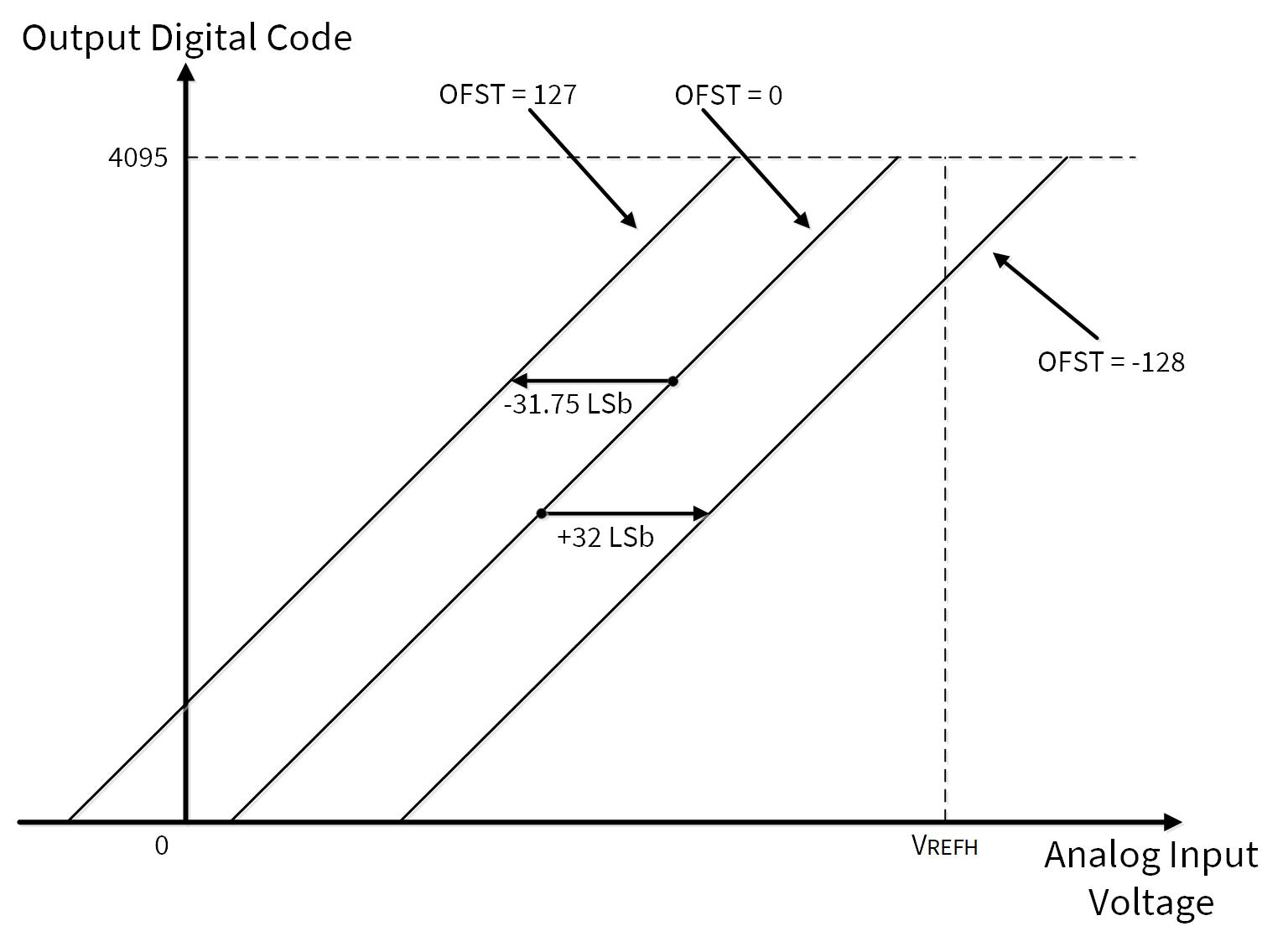
Gain adjustment direction
The ADC has a gain adjustment function to compensate for gain error.
The SARn_ANA_CAL[20:16] register can adjust the gain.
It is possible to select code from +15 to –15 in a decimal number for SARn_ANA_CAL[20:16].
The gain adjustment step is a half of 1LSb.
The equation follows (GAIN= the value of SARn_ANA_CAL[20:16]):
O u t p u t D i g i t a l C o d e = m a x 0 , min 4095 , f l o o r 4096 - G A I N V R E F H × V I N - V R E F H 2 + 2048
The relationship between the GAIN and the gain shift direction is shown in Figure 21.
Figure 21. Relationship between GAIN and gain shift direction
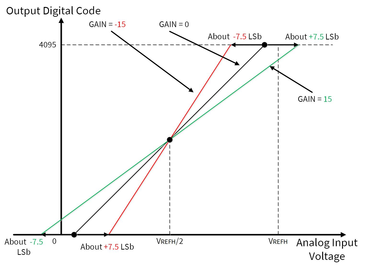
Calibration procedure
Figure 22 shows the example flowchart of ADC calibration. First adjust the offset, and next adjust the gain. If temperature sensor channel is enabled, reference buffer mode should also be enabled.
Figure 22. Example flowchart of ADC calibration
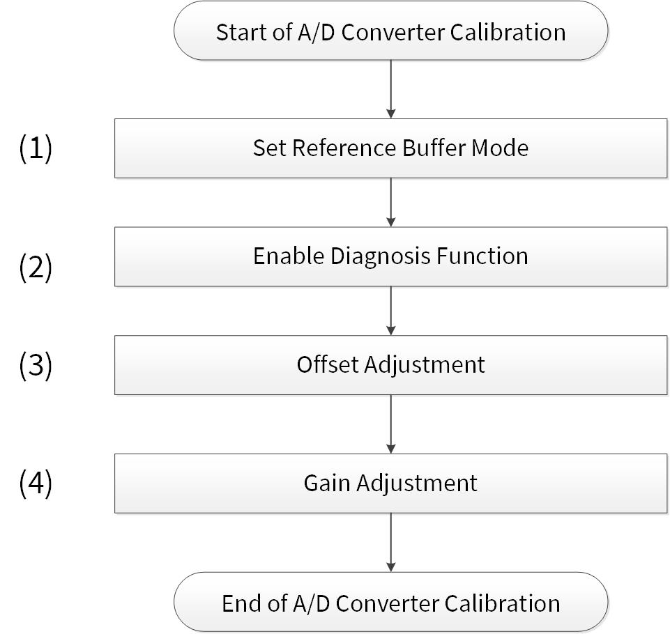
Configuration
Table 27 lists the parameters of the configuration part of in SDL for ADC calibration procedure settings.
Table 27. Parameters for ADC calibration procedure settings
Parameters | Description | Value |
|---|---|---|
| Offset calibration setting | 127ul |
| Gain calibration setting | 0ul |
| Select reference buffer mode | 1ul (See Table 25) |
| Analog macro for the potentiometer on TRAVEO™ T2G baseboard | CY_ADC_POT_MACRO: PASS0_SAR0 |
Functions | Description | Value |
|---|---|---|
| Sets the ePASS MMIO reference buffer mode | RefBufMode = CY_ADC_REF_BUF_MODE_ON |
| Enables the diagnosis function | AnalogMacro = BB_POTI_ANALOG_MACRO |
Sample code
See Code Listing 33 for a sample code for initial configuration of ADC calibration procedure settings.
Code Listing 33 ADC calibration procedure settings
    :
    /* Calibration Setting */
    cy_stc_adc_analog_calibration_conifg_t calibrationConfig =
    {
        .offset = 127ul,/* Offset Calibration Setting */
        .gain   = 0ul,/* Gain Calibration Setting */
    };
    :
    int main(void)
    {
        __enable_irq(); /* Enable global interrupts. */

        SystemInit();

    :
        /* Set ePASS MMIO reference buffer mode */  /* (1) Set REF_BUF MODE. See Code Listing 30. */
        Cy_Adc_SetReferenceBufferMode(PASS0_EPASS_MMIO,CY_ADC_REF_BUF_MODE_ON);
        /* Enable diag function. */
        Cy_Adc_Diag_Enable(BB_POTI_ANALOG_MACRO);  /* (2) Enable ADC Diagnosis. See Code Listing 31. */
    :
        if(Offset_Calibration() == true)  /* (3) Offset Adjustment. */
        {
            //Gain_Status = Gain_Calibration();
            if(Gain_Calibration() == true)  /* (4) Gain Adjustment. */
            {
                /* Test Completed */
                while(1);
            }
            else
            {
                /* Error */
                while(1);
            }
        }
        else
        {
            /* Error */
            while(1);
        }
    }
Offset adjustment procedure
Figure 23 shows the flowchart of offset adjustment.
Figure 23. Example flowchart of offset adjustment
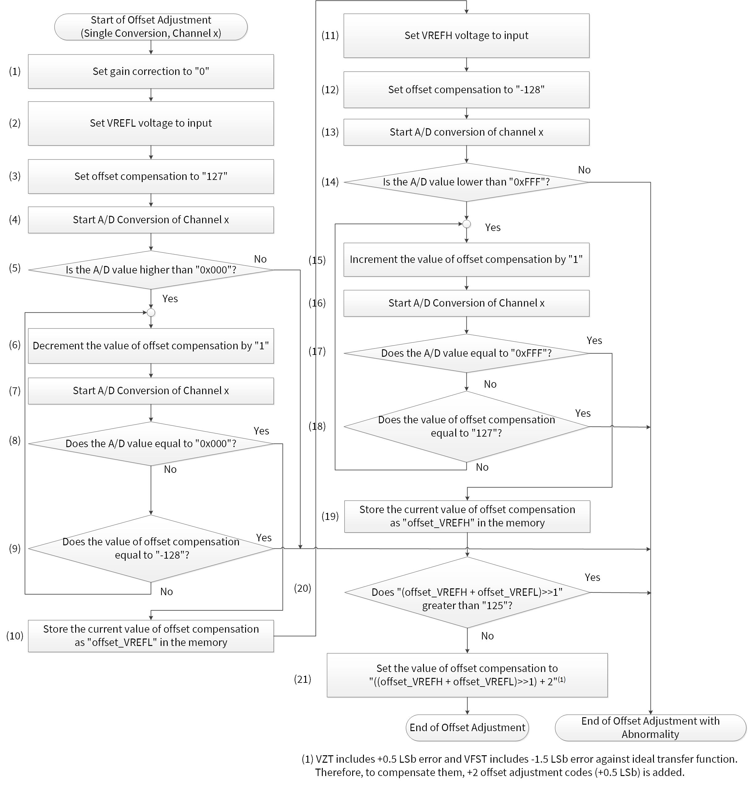
Use case
The following use case is an example of offset adjustment using ADC logical channel 0.
Configuration
Table 29 lists the parameters and Table 30 lists the functions of the configuration part of in SDL for offset adjustment procedure settings.
Table 29. Parameters for offset adjustment procedure settings
Parameters | Description | Value |
|---|---|---|
| Analog macro for the potentiometer on the TRAVEO™ T2G baseboard | CY_ADC_POT_MACRO: PASS0_SAR0 |
| Select reference buffer mode | 1ul (See Table 25) |
| Calibration offset value | -128 or more, 127 or less |
| Conversion result buffer | - (Calculated Value) |
Table 30. Functions for offset adjustment procedure settings
Functions | Description | Value |
|---|---|---|
| Issues a software start trigger | PASS SARchannel = &BB_POTI_ANALOG_MACRO->CH[ADC_LOGICAL_CHANNEL] |
| Returns the group conversion status | PASS SARchannel = &BB_POTI_ANALOG_MACRO->CH[ADC_LOGICAL_CHANNEL] |
| Gets the conversion result and status | SAR Channel = BB_POTI_ANALOG_MACRO->CH[ADC_LOGICAL_CHANNEL], Result = &resultBuff, Status = &statusBuff |
| Sets the analog calibration value | PASS SARchannel = &BB_POTI_ANALOG_MACRO->CH[ADC_LOGICAL_CHANNEL] Calibration Configure = calibrationConfig |
| Initializes the ADC channel | PASS SARchannel = &BB_POTI_ANALOG_MACRO->CH[ADC_LOGICAL_CHANNEL] ADCchannel Configure = adcChannelConfig |
| Sets ePASS MMIO reference buffer mode | RefBufMode = CY_ADC_REF_BUF_MODE_ON |
| Enables the diagnosis function | AnalogMacro = BB_POTI_ANALOG_MACRO |
| Enables the corresponding channel | PASS SARchannel = &BB_POTI_ANALOG_MACRO->CH[ADC_LOGICAL_CHANNEL] |
Sample code
See Code Listing 34 to Code Listing 35 for sample code snippets for initial configuration of offset adjustment procedure settings.
Code Listing 34 Offset adjustment procedure settings
:
#define BB_POTI_ANALOG_MACRO        CY_ADC_POT_MACRO
:
/* Calibration Setting */
cy_stc_adc_analog_calibration_conifg_t calibrationConfig =
{
    .offset = 127ul,/* Offset Calibration Setting */
    .gain   = 0ul,/* Gain Calibration Setting */
};
:
int main(void)
{
    __enable_irq(); /* Enable global interrupts. */

    SystemInit();

:
    /* Set Gain Coreection to 0" */
    calibrationConfig.gain = 0ul;  /* (1) Set Gain Correction to “0”. */
    /* Set VREFL Voltage to Input */
    adcChannelConfig.pinAddress = CY_ADC_PIN_ADDRESS_VREF_L;  /* (2) Set VREFL Voltage to Input. */
    /* Set Offset Compensation to "127" */
    calibrationConfig.offset = 127ul;  /* (3) Set offset compensation to “127”. */
:
     if(Offset_Calibration() == true)  /* (4) Start A/D Conversion of Channel x. */
    {
        //Gain_Status = Gain_Calibration();
        if(Gain_Calibration() == true)
        {
            /* Test Completed */
            while(1);
        }
        else
        {
            /* Error */
            while(1);
        }
    }
    else
    {
        /* Error */
        while(1);
    }
}

/*********************************************************************/
/* Function: GetAdcValue                                             */
/*********************************************************************/
uint16_t GetAdcValue(void)
{
    /* trigger ADC */
    Cy_Adc_Channel_SoftwareTrigger(&BB_POTI_ANALOG_MACRO->CH[ADC_LOGICAL_CHANNEL]);  /* Software Trigger Setting. See Code Listing 9. */h

    /* wait ADC completion */
    Cy_SysTick_DelayInUs(10000);
    cy_stc_adc_group_status_t Groupstatus = { false };

    do{
    Cy_Adc_Channel_GetGroupStatus(&BB_POTI_ANALOG_MACRO->CH[ADC_LOGICAL_CHANNEL],&Groupstatus);  /* Returns A/D conversion status. See Code Listing 32. */
}while(Groupstatus.grpComplete == false);


    /* Get the result(s) */
    Cy_Adc_Channel_GetResult(&BB_POTI_ANALOG_MACRO->CH[ADC_LOGICAL_CHANNEL], &resultBuff, &statusBuff);  /* Read A/D conversion data. See Code Listing 11. */
    return resultBuff;
}
/*********************************************************************/
/* Function: OffsetCalibration                                       */
/*********************************************************************/
bool Offset_Calibration(void)
{
    /* Start A/D Conversion and get the A/D value */
    result = GetAdcValue();

    /* Is the A/D Value Higher than 0 ? */  /* (5) Is the A/D value higher than “0x000” ? */
    if(result > 0)
    {
        /* Decrment the Value of Offset Compensation by "1" */  /* (6) Decrement the value of offset compensation by “1”. */
        for(offset_VREFL = 127; offset_VREFL >= -128; offset_VREFL -= 1)
        {
            /* Set "offset_VREFL" to offset regist value */
            calibrationConfig.offset = offset_VREFL;
            Cy_Adc_SetAnalogCalibrationValue(BB_POTI_ANALOG_MACRO, &calibrationConfig);  /* Analog Calibration Value Setting. See Code Listing 35. */


            /* Get AD Value */
            result = GetAdcValue();  /* (7) Start A/D Conversion of Channel x. */


            /* Does the A/D value Equal to 0 ? */
            if(result == 0)  /* (8) Does the A/D value equal to “0x000” ? */
            {
                break;  /* (10) Store the current value of offset compensation as “offset_VREFL” in the memory. */
            }


            if(offset_VREFL == -128)  /* (9) Does the value of offset compensation equal to “-128”? */
            {
                /* Error */
                return false;
            }
}
}
    else
    {
        /* result <= 0x000 */
        /* End of Offset Adjustment with Abnormality */
        return false;
    }


    /*  Setting for VREFH */
    /* Set VREFH Voltage to Input */
    /* /* (11) Set VREFH voltage to input. */
    adcChannelConfig.pinAddress = CY_ADC_PIN_ADDRESS_VREF_H;
    /* Set Offset Compensation to "-128" */
    calibrationConfig.offset = -128;  /* (12) Set offset compensation to “-128”. */
    Cy_Adc_SetAnalogCalibrationValue(BB_POTI_ANALOG_MACRO, &calibrationConfig);  /* Analog Calibration Value Setting. See Code Listing 35. */


    Cy_Adc_Channel_Init(&BB_POTI_ANALOG_MACRO->CH[ADC_LOGICAL_CHANNEL], &adcChannelConfig);  /* ADC Channel Initialize. See Code Listing 5. */

    /* Enable ADC ch. */

    Cy_Adc_Channel_Enable(&BB_POTI_ANALOG_MACRO->CH[ADC_LOGICAL_CHANNEL]);  /* Enable ADC Channel. See Code Listing 8. */

    /* Start A/D Conversion and get the A/D value */

    result = GetAdcValue();  /* (13) Start A/D Conversion of Channel x. */

    /* Is the AD value lower than 0xFFF */


    if(result < 0xFFF)  /* (14) Is the A/D value lower than “0xFFF”? */
    {
        /* Increment the Value of Offset Compensation by "1" */
        for(offset_VREFH = -128; offset_VREFH <= 127; offset_VREFH += 1)  /* (15) Increment the value of offset compensation by “1” */
        {


            /* Set "offset_VREFH" to offset regist value */
            calibrationConfig.offset = offset_VREFH;
            Cy_Adc_SetAnalogCalibrationValue(BB_POTI_ANALOG_MACRO, &calibrationConfig);  /* Analog Calibration Value Setting. See Code Listing 35. */


            /* Get AD Value */
            result = GetAdcValue();  /* (16) Start A/D Conversion of Channel x. */


            /* Does the A/D value Equal to 4095 ? */
            if(result == 0xFFF)  /* (17) Does the A/D value equal to “0xFFF” ? */
            {
                break;  /* (19) Store the current value of offset compensation as “offset_VREFH” in the memory. */
            }


            /* Does the value of offset compensation equal to "127" ? */
     if(offset_VREFH == 127)  /* (18) Does the value of offset compensation equal to “127”? */
            {
                /* End of Offset Adjustment with Abnormality */
                return false;
            }
        }
    }
    else
    {
        /* End of Offset Adjustment with Abnormality */
        return false;
    }

    /* Does "(offset_VREFH+offset_VREFL)>>1" greater than "125" ?*/
    int32_t Value = (offset_VREFH+offset_VREFL)>>1;
    if(Value > 125)  /* (20) Does “(offset_VREFH + offset_VREFL)>>1” greater than “125”? */
    {


        /* End of Offset Adjustment with Abnormality */
        return false;
    }

    /* Set the value of offset compensation to ((offset_VREFH+offset_VREFL)>>1) + 2 */
    calibrationConfig.offset = ((offset_VREFH+offset_VREFL)>>1) + 2;  /* (21) Set the value of offset compensation to “((offset_VREFH + offset_VREFL)>>1) + 2” */

    return true;

}
Code Listing 35 Cy_Adc_SetAnalogCalibrationValue() function
    cy_en_adc_status_t Cy_Adc_SetAnalogCalibrationValue(volatile stc_PASS_SAR_t * base, cy_stc_adc_analog_calibration_conifg_t * config)
    {
        cy_en_adc_status_t    ret      = CY_ADC_SUCCESS;
        un_PASS_SAR_ANA_CAL_t unAnaCal = { 0ul };

        if (NULL != config)
        {
            unAnaCal.stcField.u8AOFFSET = config->offset;
            unAnaCal.stcField.u5AGAIN   = config->gain;
            base->unANA_CAL.u32Register = unAnaCal.u32Register;
        }
        else
        {
            ret = CY_ADC_BAD_PARAM;
        }
        return ret;
    }
Gain adjustment procedure
Figure 24 shows the flowchart of gain adjustment.
Figure 24. Example flowchart of gain adjustment
Use case
The following use case is an example of gain adjustment using ADC logical channel 0.
Configuration
Table 31 lists the parameters and Table 32 lists the functions of the configuration part of in SDL for ADC global settings.
Table 31. Parameters for gain adjustment procedure settings
Parameters | Description | Value |
|---|---|---|
| Analog macro for the potentiometer on the TRAVEO™ T2G baseboard | CY_ADC_POT_MACRO: PASS0_SAR0 |
| Calibration gain value | -15 or more, 15 or less |
| Conversion result buffer | - (Calculated Value) |
Table 32. Functions for gain adjustment procedure settings
Functions | Description | Value |
|---|---|---|
| Issues a software start trigger | PASS SARchannel = &BB_POTI_ANALOG_MACRO->CH[ADC_LOGICAL_CHANNEL] |
| Returns the group conversion status | PASS SARchannel = &BB_POTI_ANALOG_MACRO->CH[ADC_LOGICAL_CHANNEL] |
| Gets the conversion result and status | SAR Channel = BB_POTI_ANALOG_MACRO->CH[ADC_LOGICAL_CHANNEL], Result = &resultBuff, Status = &statusBuff |
| Sets the analog calibration value | PASS SARchannel = &BB_POTI_ANALOG_MACRO->CH[ADC_LOGICAL_CHANNEL] Calibration Configure = calibrationConfig |
| Initializes the ADC channel | PASS SARchannel = &BB_POTI_ANALOG_MACRO->CH[ADC_LOGICAL_CHANNEL] ADCchannel Configure = adcChannelConfig |
| Enables the corresponding channel | PASS SARchannel = &BB_POTI_ANALOG_MACRO->CH[ADC_LOGICAL_CHANNEL] |
Sample code
See Code Listing 36 for sample code for initial configuration of gain adjustment procedure settings
Code Listing 36 Gain adjustment procedure settings
   :
   #define BB_POTI_ANALOG_MACRO        CY_ADC_POT_MACRO
   :
   /* Calibration Setting */
   cy_stc_adc_analog_calibration_conifg_t calibrationConfig =
   {
       .offset = 127ul,/* Offset Calibration Setting */
       .gain   = 0ul,/* Gain Calibration Setting */
   };
   :
   int main(void)
   {
       __enable_irq(); /* Enable global interrupts. */

       SystemInit();

   :
       if(Offset_Calibration() == true)
       {
           //Gain_Status = Gain_Calibration();
           if(Gain_Calibration() == true)
           {
               /* Test Completed */
               while(1);
           }
           else
           {
               /* Error */
               while(1);
           }
       }
       else
       {
           /* Error */
           while(1);
       }
   }


   /*********************************************************************/
   /* Function: GetAdcValue                                             */
   /*********************************************************************/
   uint16_t GetAdcValue(void)
   {
       /* trigger ADC */
       Cy_Adc_Channel_SoftwareTrigger(&BB_POTI_ANALOG_MACRO->CH[ADC_LOGICAL_CHANNEL]);  /* Software Trigger Setting. See Code Listing 9. */


       /* wait ADC completion */
       Cy_SysTick_DelayInUs(10000);
       cy_stc_adc_group_status_t Groupstatus = { false };

       do{
       Cy_Adc_Channel_GetGroupStatus(&BB_POTI_ANALOG_MACRO->CH[ADC_LOGICAL_CHANNEL],&Groupstatus);  /* Returns A/D conversion status. See Code Listing 32. */
   }while(Groupstatus.grpComplete == false);
       /* Get the result(s) */
       Cy_Adc_Channel_GetResult(&BB_POTI_ANALOG_MACRO->CH[ADC_LOGICAL_CHANNEL], &resultBuff, &statusBuff);  /* Read A/D conversion data. See Code Listing 11. */

       return resultBuff;
   }

   /*********************************************************************/
   /* Function: Gain_Calibration                                        */
   /*********************************************************************/


   bool Gain_Calibration(void)
   {
       int16_t Gain;
       /* Set Gain Correction setting to "15" */  /* (1) Set Gain Correction to “15”. */
       calibrationConfig.gain = 15;
       /* Set VREFL Voltage to Input */
       adcChannelConfig.pinAddress = CY_ADC_PIN_ADDRESS_VREF_L;  /* (2) Set VREFL Voltage to Input. */
       Cy_Adc_SetAnalogCalibrationValue(BB_POTI_ANALOG_MACRO, &calibrationConfig);  /* Analog Calibration Value Setting. See Code Listing 35. */
       Cy_Adc_Channel_Init(&BB_POTI_ANALOG_MACRO->CH[ADC_LOGICAL_CHANNEL], &adcChannelConfig);  /* Initialize ADC Channel. See Code Listing 5. */


       /* Enable ADC ch. */
       Cy_Adc_Channel_Enable(&BB_POTI_ANALOG_MACRO->CH[ADC_LOGICAL_CHANNEL]);  /* Enable ADC Channel. See Code Listing 8 */
       /* Start A/D value Conversion */
       result = GetAdcValue();  /* (3) Start A/D Conversion of Channel x. */


       if(result > 0)  /* (4) Is the A/D value higher than “0x000”? */
       {
            for(Gain = 15; Gain >=-14; Gain -= 1)
            {


               /* Set gain to register */
               calibrationConfig.gain = Gain;  /* Analog Calibration Value Setting. See Code Listing 35. */
               Cy_Adc_SetAnalogCalibrationValue(BB_POTI_ANALOG_MACRO, &calibrationConfig);


               result = GetAdcValue();  /* (5) Start A/D Conversion of Channel x. */


               /* Does the A/D value equal to "0" ?*/
               if(result == 0)  /* (6) Does the A/D value equal to “0x000”?  */
               {

                   /* Set gain compension to "gain" -1 */
                   calibrationConfig.gain = Gain - 1;  /* (7) Set gain compensation to “the current value - 1". */
                   Cy_Adc_SetAnalogCalibrationValue(BB_POTI_ANALOG_MACRO, &calibrationConfig);  /* Analog Calibration Value Setting. See Code Listing 35. */

                   break;
               }


               if( Gain == -14)  /* (8) Does the value of gain compensation equal to “-14” */
               {
               /* End of Offset Adjustment with Abnormality */
                   return false;
               }
       }
       return true;
   }
Temperature sensor
The temperature sensor can measure the chip temperature using an ADC. To accurately measure the temperature at run time, use the reference measurement done during production. This reference data is stored in SFlash along with other calibration data. See the “SAR ADC” chapter of the architecture TRM for the exact address to read this data.
This section shows an example chip temperature measurement flow.
Ensure that you have configured the settings as described in the Basic ADC global settings section.
Temperature measurement procedure
Figure 25 shows the example flowchart of the chip temperature measurement.
Figure 25. Example flowchart of temperature measurement

- ADC calibration: See 9.3 for example of offset and gain adjustment.
- Check VREFH and VREL: See 8.2 for example of VREFH and VREFL diagnosis.
- Set the reference buffer mode: Set the PASS_CTL register to enable reference buffer mode.
- Set the temperature sensor register: Set bit 9, 8 and 6 of PASS_TEST_CTL register to ‘1’ only for CYT2B. For other devices, keep the default value.
- Read the bandgap reference (VBG) using ADC: Store the A/D conversion result of VBG.
- Read the temperature sensor output (VBE) using ADC: Store the A/D conversion result of VBE. To find the proper sample time for the temperature sensor, see the datasheet mentioned in 1.
- Calculate the internal chip temperature:
- VBE (temperature sensor output) has a second-order dependency on temperature (T) and can be described by the following equation: V B E = a T 2 + b T + c
To calculate the temperature from VBE, you must know the coefficients (a, b, and c) of the above equation. These coefficients can be calculated using the data (VBE measured at three different temperatures) stores in SFlash. See the architecture TRM for details. The three combinations of (VBE, T) to be used depends on the supply voltage (VDDA). For example, to calculate polynomial coefficients:
When VDDA = 3.3 V, use SFlash data set#0 and set#1 in the architecture TRM
When VDDA = 5.0 V, use SFlash data set#0 and set#2 in the architecture TRM
- Because the ADC reference voltage may have changed from the calibration, VBE must be scaled using the ratio of the bandgap voltage at ROOM temperature using ADC (VBG_S3)and VBG, where before it is used to calculate the temperature.
- Calculate temperature using the above polynomial: V B E _ N E W = a T 2 + b T + c
- After calculating the temperature, the accuracy can be improved by using the bandgap reference from the nearest temperature in step 7.b. Essentially, if the temperature calculated in step 7.c is close to:
- COLD (-40), repeat step 7.b with the bandgap voltage at COLD temperature using ADC (VBG_S2) and recalculate the temperature using step 7.c(7.3).
- HOT (150), repeat step 7.b with the bandgap voltage at HOT temperature using ADC (VBG_CHI) and recalculate the temperature using step 7.c.
- ROOM (27), temperature calculated in step 7.c is the final temperature.
Use case
- VDDDA = 5.0 V
- ADC logical channel: 0
- Number of iterations to get the ADC readings: 16
- Sampling time: 120 ADC clock cycles
Configuration
Table 33 lists the parameters and Table 34 lists the functions of the configuration part of in SDL for the temperature measurement.
Table 33. Parameters for temperature measurement
Parameters | Description | Value |
|---|---|---|
| Select the analog power rails. 3.3 V: USE_TRIM_FOR_3P3V_VDDA 5.0 V: USE_TRIM_FOR_5P0V_VDDA | USE_TRIM_FOR_5P0V_VDDA |
| ADC logical channel to be used | 0ul |
| Number of iterations to get the ADC readings | 16ul |
| Sample time in ADC clock cycles | 120ul |
| Trigger OFF | 0ul (See Table 3) |
| Channel priority | 0ul |
| Pre-emption type | 3ul (See Table 3) |
| Is group end? | True |
| Done level | 0ul (See Table 3) |
| Pin address | channelAddress |
| Port address | 0ul (See Table 3) |
| External MUX select | 0ul |
| Enables external MUX | True |
| Pre-condition mode | 0ul (See Table 3) |
| Overlap diagnostics mode | 0ul (See Table 3) |
| Sample time | ADC_CH_SAMPLE_TIME |
| Calibration value select | 1ul (See Table 3) |
| Post processing mode | 1ul (See Table 3) |
| Result alignment | 0ul (See Table 3) |
| Sign extension | 0ul (See Table 3) |
| Average count | (ADC_CH_NUM_OF_ITERATION-1) |
| Right shift | 0ul |
| Range detection mode | 1ul (See Table 3) |
| Range detection low threshold | 0x0000ul |
| Range detection high threshold | 0x0FFFul |
| Mask group done | True |
| Mask group cancelled | False |
| Mask group overflow | False |
| Mask channel range | False |
| Mask channel pulse | False |
| Mask channel overflow | False |
Table 34. Functions for temperature measurement
Functions | Description | Value |
|---|---|---|
| Reads the ADC conversion result of the target pin address | CY_ADC_IN_VBG (Y_ADC_PIN_ADDRESS_VBG = 38ul), CY_ADC_IN_TEMP (CY_ADC_PIN_ADDRESS_VTEMP = 39ul) |
| Initializes and enables the ADC channel | |
| Calculates the chip temperature | &tempRefValue, &tempRawValue |
Sample code
See Code Listing 37 to Code Listing 41 for sample code of temperature measurement.
Code Listing 37 Temperature measurement settings
    /** Select the analaog power rails as per your hardware */
    #define USE_TRIM_FOR_3P3V_VDDA                  0ul
    #define USE_TRIM_FOR_5P0V_VDDA                  1ul
    #define USE_TEMPERATURE_TRIM_VALUES             USE_TRIM_FOR_5P0V_VDDA

    /** Read from the SFLASH table */
    #if (USE_TEMPERATURE_TRIM_VALUES == USE_TRIM_FOR_3P3V_VDDA)
        /** SFLASH table for VDDA - 3.3V */
        #define EPASS_TEMP_TRIM_TEMP_COLDSORT       0x17000654ul
        #define EPASS_TEMP_TRIM_TEMP_ROOMSORT       0x1700064Eul
        #define EPASS_TEMP_TRIM_TEMP_HOTCLASS       0x1700065Aul
        #define EPASS_TEMP_TRIM_DIODE_COLDSORT      0x17000656ul
        #define EPASS_TEMP_TRIM_DIODE_ROOMSORT      0x17000650ul
        #define EPASS_TEMP_TRIM_DIODE_HOTCLASS      0x1700065Cul
        #define EPASS_TEMP_TRIM_VBG_COLDSORT        0x17000658ul
        #define EPASS_TEMP_TRIM_VBG_ROOMSORT        0x17000652ul
        #define EPASS_TEMP_TRIM_VBG_HOTCLASS        0x1700065Eul
    #else
    /** SFLASH table for VDDA - 5V */
        #define EPASS_TEMP_TRIM_TEMP_COLDSORT       0x17000654ul
        #define EPASS_TEMP_TRIM_TEMP_ROOMSORT       0x1700064Eul
        #define EPASS_TEMP_TRIM_TEMP_HOTCLASS       0x1700065Aul
        #define EPASS_TEMP_TRIM_DIODE_COLDSORT      0x1700066Eul
        #define EPASS_TEMP_TRIM_DIODE_ROOMSORT      0x1700066Aul
        #define EPASS_TEMP_TRIM_DIODE_HOTCLASS      0x17000672ul
        #define EPASS_TEMP_TRIM_VBG_COLDSORT        0x17000670ul
        #define EPASS_TEMP_TRIM_VBG_ROOMSORT        0x1700066Cul
        #define EPASS_TEMP_TRIM_VBG_HOTCLASS        0x17000674ul
    #endif  /* (USE_TEMPERATURE_TRIM_VALUES == USE_TRIM_FOR_3P3V_VDDA) */

    /** SFLASH table read macro */
    #define GET_SFLASH_VALUE(x)                     CY_GET_REG16(x)
    #define GET_TRIM_VALUE(x)                       (GET_SFLASH_VALUE(x) & 0xFFFFu)

    /** Temperature trim values read from SFLASH */
    #define TEMP_TRIM_TEMP_ROOMSORT                 GET_TRIM_VALUE(EPASS_TEMP_TRIM_TEMP_ROOMSORT)
    #define TEMP_TRIM_TEMP_COLDSORT                 GET_TRIM_VALUE(EPASS_TEMP_TRIM_TEMP_COLDSORT)
    #define TEMP_TRIM_TEMP_HOTCLASS                 GET_TRIM_VALUE(EPASS_TEMP_TRIM_TEMP_HOTCLASS)

    #define TEMP_TRIM_DIODE_ROOMSORT                GET_TRIM_VALUE(EPASS_TEMP_TRIM_DIODE_ROOMSORT)
    #define TEMP_TRIM_DIODE_COLDSORT                GET_TRIM_VALUE(EPASS_TEMP_TRIM_DIODE_COLDSORT)
    #define TEMP_TRIM_DIODE_HOTCLASS                GET_TRIM_VALUE(EPASS_TEMP_TRIM_DIODE_HOTCLASS)

    #define TEMP_TRIM_VBG_ROOMSORT                  GET_TRIM_VALUE(EPASS_TEMP_TRIM_VBG_ROOMSORT)
    #define TEMP_TRIM_VBG_COLDSORT                  GET_TRIM_VALUE(EPASS_TEMP_TRIM_VBG_COLDSORT)
    #define TEMP_TRIM_VBG_HOTCLASS                  GET_TRIM_VALUE(EPASS_TEMP_TRIM_VBG_HOTCLASS)

    /**
     * Macro definition for ADC instance and Temperature measurement channels
     */

    /** ADC instance, clock and irq configuration macro */
    #define CY_ADC_MACRO                            PASS0_SAR0
    #define CY_ADC_MMIO_MACRO                       PASS0_EPASS_MMIO
    #define CY_ADC_PCLK                             PCLK_PASS0_CLOCK_SAR0
    #define CY_ADC_IRQN                             pass_0_interrupts_sar_0_IRQn

    /** ADC channels for diode and temperature measurements */
    #define CY_ADC_IN_VBG                           CY_ADC_PIN_ADDRESS_VBG
    #define CY_ADC_IN_TEMP                          CY_ADC_PIN_ADDRESS_VTEMP

    /** ADC logical channel to be used */
    #define ADC_LOGICAL_CHANNEL                     0ul

    /** Number of iteration to get the ADC readings */
    #define ADC_CH_NUM_OF_ITERATION                 16ul

    /** Sample time for sampling ADC channel */
    #define ADC_CH_SAMPLE_TIME                      120ul

    /** Defines low and high range for range detection mode */
    #define ADC_CH_RANGE_DETECT_LOW                 0x0000ul
    #define ADC_CH_RANGE_DETECT_HIGH                0x0FFFul

    /** Select the internal current requirement for the die-temperature sensor
        0->1uA, 2->2uA, 3->5uA, 3->10uA */
    #define ADC_CAL_TS_CUR_SEL_VALUE                3ul
    #define ADC_CAL_TS_CUR_SEL_OFFSET               8ul
    #define ADC_CAL_TS_CUR_SEL_MASK             (ADC_CAL_TS_CUR_SEL_VALUE << ADC_CAL_TS_CUR_SEL_OFFSET)

    /** Select current or voltage output from the die-temperature sensor
    	0->current, 1->voltage */
    #define ADC_CAL_TS_VI_SEL_VALUE               1ul
    #define ADC_CAL_TS_VI_SEL_OFFSET              6ul
    #define ADC_CAL_TS_VI_SEL_MASK               (ADC_CAL_TS_VI_SEL_VALUE << ADC_CAL_TS_VI_SEL_OFFSET)

    /** Setup test calibration register to measure the die-temperature */
    #define ADC_CAL_TEMP_TEST_CTL_ADDR_OFFSET       (0x80)
    #define ADC_CAL_TEMP_TEST_CTL_ADDR  (uint32_t)CYREG_PASS0_PASS_CTL + ADC_CAL_TEMP_TEST_CTL_ADDR_OFFSET)
    #define ADC_CAL_TEMP_TEST_CTL_MASK              (ADC_CAL_TS_CUR_SEL_MASK | ADC_CAL_TS_VI_SEL_MASK)


    /******************************************************************************/
    /* Global Variables                                                           */
    /******************************************************************************/
    :
    /**
     * \var cy_stc_adc_channel_config_t adcChannelConfig
     * \brief ADC channel configuration structure
     */
    cy_stc_adc_channel_config_t adcChannelConfig =
    {
        .triggerSelection          = CY_ADC_TRIGGER_OFF,
        .channelPriority           = 0ul,
        .preenptionType            = CY_ADC_PREEMPTION_FINISH_RESUME,
        .isGroupEnd                = true,
        .doneLevel                 = CY_ADC_DONE_LEVEL_PULSE,
        .pinAddress                = CY_ADC_PIN_ADDRESS_VREF_L,
        .portAddress               = CY_ADC_PORT_ADDRESS_SARMUX0,
        .extMuxSelect              = 0ul,
        .extMuxEnable              = true,
        .preconditionMode          = CY_ADC_PRECONDITION_MODE_OFF,
        .overlapDiagMode           = CY_ADC_OVERLAP_DIAG_MODE_OFF,
        .sampleTime                = ADC_CH_SAMPLE_TIME,
        .calibrationValueSelect    = CY_ADC_CALIBRATION_VALUE_ALTERNATE,
        .postProcessingMode        = CY_ADC_POST_PROCESSING_MODE_AVG,
        .resultAlignment           = CY_ADC_RESULT_ALIGNMENT_RIGHT,
        .signExtention             = CY_ADC_SIGN_EXTENTION_UNSIGNED,
        .averageCount              = (ADC_CH_NUM_OF_ITERATION-1),
        .rightShift                = 0ul,
        .rangeDetectionMode        = CY_ADC_RANGE_DETECTION_MODE_INSIDE_RANGE,
        .rangeDetectionLoThreshold = ADC_CH_RANGE_DETECT_LOW,
        .rangeDetectionHiThreshold = ADC_CH_RANGE_DETECT_HIGH,
        .mask.grpDone              = true,
        .mask.grpCancelled         = false,
        .mask.grpOverflow          = false,
        .mask.chRange              = false,
        .mask.chPulse              = false,
        .mask.chOverflow           = false,
    };

    /**
     * \var static bool isConversionComplete
     * \brief ADC conversion complete flag */
    static bool isConversionComplete = false;

    /**
     * \var static uint16_t resultBuff
     * \brief ADC conversion result buffer place holder */
    static uint16_t resultBuff[ADC_CH_NUM_OF_ITERATION];

    /**
     * \var static cy_stc_adc_ch_status_t statusBuff
     * \brief ADC conversion status buffer place holder */
    static cy_stc_adc_ch_status_t  statusBuff[ADC_CH_NUM_OF_ITERATION];

    /**
     * \var static double temperatureData
     * \brief stores internal die-temperature value */
    static double temperatureData;
Code Listing 38 Temperature measurement
    int main(void)
    {
        cy_stc_adc_temp_ref_t tempRefValue;
        cy_stc_adc_temp_raw_t tempRawValue;

        /* Enable global interrupts. */
        __enable_irq();

        SystemInit();
    :
        /* Update the sort temperature value matrix A */
        tempRefValue.adcTempValues.coldValue = -(TEMP_TRIM_TEMP_COLDSORT / 10.0);
        // Note: Temperature data read from sFLASH is multiple of 10.
        tempRefValue.adcTempValues.roomValue = (TEMP_TRIM_TEMP_ROOMSORT / 10.0);
        // Note: Temperature data read from sFLASH is multiple of 10.
        tempRefValue.adcTempValues.hotValue = (TEMP_TRIM_TEMP_HOTCLASS / 10.0);
        // Note: Temperature data read from sFLASH is multiple of 10.

        /* Update the sort temperature adc value matrix b */
        tempRefValue.adcDiodeValues.coldValue = (uint16_t)TEMP_TRIM_DIODE_COLDSORT;
        tempRefValue.adcDiodeValues.roomValue = (uint16_t)TEMP_TRIM_DIODE_ROOMSORT;
        tempRefValue.adcDiodeValues.hotValue = (uint16_t)TEMP_TRIM_DIODE_HOTCLASS;

        /* Update the reference Vbg values */
        tempRefValue.adcVbgValues.coldValue = (uint16_t)TEMP_TRIM_VBG_COLDSORT;
        tempRefValue.adcVbgValues.roomValue = (uint16_t)TEMP_TRIM_VBG_ROOMSORT;
        tempRefValue.adcVbgValues.hotValue = (uint16_t)TEMP_TRIM_VBG_HOTCLASS;

        /* This block needs to be called every time when reading the die temperature */
        {
            /* SoftTrim API */
            AdcCalculateSoftTrim(CY_ADC_MACRO);  /* (1) ADC calibration. See Code Listing 33. */

            /* Test with the updatded calibration values */
            AdcCheckSoftTrim();  /* (2) Check VREFH and VREFL. See Code Listing 29. */

            /* Set reference buffered mode on - to pump Vbg from SRSS */
            Cy_Adc_SetReferenceBufferMode(CY_ADC_MMIO_MACRO, CY_ADC_REF_BUF_MODE_ON);  /* (3) Set the reference buffer mode. See Code Listing 30. */


            /* Set current configuration for temperature sensor to 10uA for better accuracy */
            CY_SET_REG32(ADC_CAL_TEMP_TEST_CTL_ADDR, ADC_CAL_TEMP_TEST_CTL_MASK);  /* (4) Set the temperature sensor register only for CYT2B. */


            /* Read and update the raw values for VBG and Temp Sensor */
            tempRawValue.adcVbgRawValue = AdcReadChannelData(CY_ADC_IN_VBG);  /* (5) Read the bandgap reference using ADC. See Code Listing 39. */


            tempRawValue.adcVtempRawValue = AdcReadChannelData(CY_ADC_IN_TEMP);  /* (6) Read the temperature sensor output using ADC. See Code Listing 39 */


            /* Calculate the internal die temperature */
            temperatureData = Cy_Adc_CalculateDieTemperature(&tempRefValue, &tempRawValue);  /* (7) Calculate the internal chip temperature. See Code Listing 41. */
        }

        for(;;)
        {
            if(temperatureData == 0.0)
            {
                /* Reaching here means SFLASH doesn't have valid values */
                CY_ASSERT(false);
            }
        }
    }
Code Listing 39 AdcReadChannelData() function
    static uint16_t AdcReadChannelData(cy_en_adc_pin_address_t channelAddress)
    {
        unsigned long avgAdcValue = 0ul;

        AdcConfigureChannel(channelAddress);  /* See [Code Listing 40](#code-listing-40-adcconfigurechannel-function). */
        {
            Cy_Adc_Channel_SoftwareTrigger(&CY_ADC_MACRO->CH[ADC_LOGICAL_CHANNEL]);  /* See Code Listing 9. */
            while(isConversionComplete != true);
            isConversionComplete = false;
            avgAdcValue += resultBuff[0];

        }
        return (avgAdcValue/ADC_CH_NUM_OF_ITERATION);
    }
Code Listing 40 AdcConfigureChannel() function
    static void AdcConfigureChannel(cy_en_adc_pin_address_t channelAddress)
    {
        /* Configure the ADC channel to requested address */
        adcChannelConfig.pinAddress = channelAddress;  /* ADC Channel Initialize. See Code Listing 5. */
        Cy_Adc_Channel_Init(&CY_ADC_MACRO->CH[ADC_LOGICAL_CHANNEL], &adcChannelConfig);


        /* Enable ADC ch. */  /* Enable ADC Channel. See [Code Listing 8](#code-listing-8-cy_adc_channel_enable-function). */
        Cy_Adc_Channel_Enable(&CY_ADC_MACRO->CH[ADC_LOGICAL_CHANNEL]);
    }
Code Listing 41 Cy_Adc_CalculateDieTemperature() function
    double Cy_Adc_CalculateDieTemperature(cy_stc_adc_temp_ref_t *refValue, cy_stc_adc_temp_raw_t *rawValue)
    {
        double determinant = 0.0;
        double coefficientMatrixForSort[3][3] = {{0.0},{0.0},{0.0}};

        double sortTempMatrixA[3][3];
        double sortTempValueMatrixB[3][1];
        double sortTempCoefficeintsX[3] = {0.0};

        double coeffA, coeffB, coeffC;
        double bSqrMin4ac = 0.0;
        double tempRefValue = 0.0;
        double tempScaleValue = 0.0;
        double correctionFactor = 0.0;
        double tempRootPos, tempRootNeg = 0.0;
        double tempRangeOffset = 10; /* relate to +/- 10 degC */
        double tempInDegreeC = 0.0;

        /***************************************************************************
         * Update the class and sort matrix from the sFLASH values
         **************************************************************************/

        /* Update the sort temperature value matrix A */
        sortTempMatrixA[0][0] = 1.0;
        sortTempMatrixA[0][1] = refValue->adcTempValues.coldValue;
        sortTempMatrixA[0][2] = pow(refValue->adcTempValues.coldValue, 2.0);
        sortTempMatrixA[1][0] = 1.0;
        sortTempMatrixA[1][1] = refValue->adcTempValues.roomValue;
        sortTempMatrixA[1][2] = pow(refValue->adcTempValues.roomValue, 2.0);
        sortTempMatrixA[2][0] = 1.0;
        sortTempMatrixA[2][1] = refValue->adcTempValues.hotValue;
        sortTempMatrixA[2][2] = pow(refValue->adcTempValues.hotValue, 2.0);

        /* Update the sort temperature adc value matrix B */
        sortTempValueMatrixB[0][0] = refValue->adcDiodeValues.coldValue;
        sortTempValueMatrixB[1][0] = refValue->adcDiodeValues.roomValue;
        sortTempValueMatrixB[2][0] = refValue->adcDiodeValues.hotValue;

        /***************************************************************************
         * Get the 2nd order coefficient for sort value matrix
          /* (7.1) Get the second order coefficients (a, b, c) */
         **************************************************************************/

        /* Get the determinant of sort temperature matrix A */
        for(uint8_t i = 0u; i < 3u; i++)
        {
            determinant = determinant + (sortTempMatrixA[0][i]*(sortTempMatrixA[1][(i+1)%3]*sortTempMatrixA[2][(i+2)%3] - sortTempMatrixA[1][(i+2)%3]*sortTempMatrixA[2][(i+1)%3]));
        }

        /* Get the inverse of sort temperature matrix A */
        for(uint8_t i = 0u; i < 3u; i++)
        {
            for(uint8_t j = 0u; j < 3u; j++)
            {
                coefficientMatrixForSort[i][j] = ((sortTempMatrixA[(i+1)%3][(j+1)%3] * sortTempMatrixA[(i+2)%3][(j+2)%3]) - (sortTempMatrixA[(i+1)%3][(j+2)%3]*sortTempMatrixA[(i+2)%3][(j+1)%3]))/ determinant;
            }
        }
        for(uint8_t i = 0u; i < 3u; i++)
        {
            for(uint8_t j = 0u; j < 3u; j++)
            {
                sortTempMatrixA[i][j] = coefficientMatrixForSort[j][i];
            }
        }

        /* Calculate sort temperature coefficient matrix X = (invA)*B */
        for(uint8_t i = 0u; i < 3u; i++)
        {
            for(uint8_t j = 0u; j < 3u; j++)
            {
                sortTempCoefficeintsX[i] += (sortTempValueMatrixB[j][0]*sortTempMatrixA[i][j]);
            }
        }

        /***************************************************************************
         * Get the temperature value from the 2nd order equation
         **************************************************************************/

        /* Rearrange the coefficients for the predicted temperature formula */
        coeffA = sortTempCoefficeintsX[2];
        coeffB = sortTempCoefficeintsX[1];
        coeffC = sortTempCoefficeintsX[0];

        /* -40degC -- SORT2, 27degC -- SORT3, 130degC -- CHI and by default reference value is SORT3 */
        tempRefValue = refValue->adcVbgValues.roomValue;

        /* Conditional label for recalculating roots */
        RECALCULATE:

            /* Calculate the correction factor (k) to remove dependency of the ADC on the reference voltage */
            correctionFactor = (tempRefValue) / (rawValue->adcVbgRawValue);

            /* Scale the data in raw with k */  /* (7.2) Get the scaled VBE_NEW */
            tempScaleValue = (correctionFactor) * (rawValue->adcVtempRawValue);


            /* Calculate the predicted temperature */  /* (7.3) Calculate the temperature */
            bSqrMin4ac = ( pow(coeffB, 2.0)) - (((4.0)*(coeffA))*(coeffC - tempScaleValue));
            tempRootNeg = ((-coeffB)-(sqrtf(bSqrMin4ac))) / ((2.0)*(coeffA));
            tempRootPos = ((-coeffB)+(sqrtf(bSqrMin4ac))) / ((2.0)*(coeffA));     // this can be minimize, kept for comparition


            /* Select the root that lies between the Hot and Cold temperature sort values [-40 degC, 150 degC] */  /* (7.4) Accuracy improvement by using VBG from the nearest temperature */
            if((tempRootPos < (refValue->adcTempValues.hotValue)) && (tempRootPos > (refValue->adcTempValues.coldValue)))
            {
                /* Temperature value is positive root of the curve */
                tempInDegreeC = tempRootPos;
            }
            else if((tempRootNeg < (refValue->adcTempValues.hotValue)) && (tempRootNeg > (refValue->adcTempValues.coldValue)))
            {
                /* Temperature value is negetive root of the curve */
                tempInDegreeC = tempRootNeg;
            }
            else
            {
                /* Apt value is not found */
                tempInDegreeC = 0.0;
            }

            /* Check for the close proximity of calculated temperature with the reference temeprature values */
            if (tempInDegreeC <= ((refValue->adcTempValues.coldValue) + tempRangeOffset))
            {
                /* Use SORT2 value to scale the measured temperature */
                tempRefValue = refValue->adcVbgValues.coldValue;
                goto RECALCULATE;
            }
            else if (tempInDegreeC >= ((refValue->adcTempValues.hotValue) - tempRangeOffset))
            {
                /* Use CHI value to scale the measured temperature */
                tempRefValue = refValue->adcVbgValues.hotValue;
                goto RECALCULATE;
            }
            else if ((tempInDegreeC <= ((refValue->adcTempValues.roomValue) + tempRangeOffset))
                && (tempInDegreeC >= ((refValue->adcTempValues.roomValue) - tempRangeOffset)))
            {
                /* Use SORT3 value to scale the measured temperature */
                tempRefValue = refValue->adcVbgValues.roomValue;
            }
            else
            {
                /* Fail safe case */
            }

        return tempInDegreeC;
    }
Glossary
Terms | Description |
|---|---|
SAR ADC | Successive approximation register analog-to-digital converter |
SARMUX | Analog input multiplexer |
TCPWM | Timer, counter, and pulse width modulator |
VREFH | High reference voltage |
VREFL | Low reference voltage |
VBG | Bandgap reference voltage |
VBE | Temperature sensor output |
Related documents
The following are the TRAVEO™ T2G family series datasheets and technical reference manuals. Contact Technical support to obtain these documents.
-
Device datasheet
- CYT2B7 datasheet 32-bit Arm® Cortex®-M4F microcontroller TRAVEO™ T2G family
- CYT2B9 datasheet 32-bit Arm® Cortex®-M4F microcontroller TRAVEO™ T2G family
- CYT4BF datasheet 32-bit Arm® Cortex®-M7 microcontroller TRAVEO™ T2G family
- CYT4DN datasheet 32-bit Arm® Cortex®-M7 microcontroller TRAVEO™ T2G family (Doc No. 002-24601)
- CYT3BB/4BB datasheet 32-bit Arm® Cortex®-M7 microcontroller TRAVEO™ T2G family
- CYT3DL datasheet 32-bit Arm® Cortex®-M7 microcontroller TRAVEO™ T2G family (Doc No. 002-27763)
- CYT4EN datasheet 32-bit Arm® Cortex®-M7 microcontroller TRAVEO™ T2G family (Doc No. 002-30842)
- CYT2CL datasheet 32-bit Arm® Cortex®-M4F microcontroller TRAVEO™ T2G family (Doc No. 002- 32508)
-
Technical reference manual
- Body controller entry family
- Body controller high family
- Cluster 2D family
- TRAVEO™ T2G automotive cluster 2D family architecture technical reference manual (TRM) (Doc No. 002-25800)
- TRAVEO™ T2G automotive cluster 2D registers technical reference manual (TRM) for CYT4DN (Doc No. 002-25923)
- TRAVEO™ T2G automotive cluster 2D registers technical reference manual (TRM) for CYT3DL (Doc No. 002-29854)
- TRAVEO™ T2G automotive cluster 2D registers technical reference manual (TRM) for CYT4EN (Doc No. 002-32087)
- Cluster entry family
- TRAVEO™ T2G automotive cluster entry family architecture technical reference manual (TRM) (Doc No. 002-33175)
- TRAVEO™ T2G automotive cluster entry registers technical reference manual (TRM) (Doc No. 002-33404)
Other references
A sample driver library (SDL) including startup as sample software to access various peripherals is provided. SDL also serves as a reference to customers for drivers that are not covered by the official AUTOSAR products. The SDL cannot be used for production purposes because it does not qualify to automotive standards. The code snippets in this application note are part of the SDL. Contact Technical support to obtain the SDL.
Revision history
Document version | Date of release | Description of changes |
|---|---|---|
** | 2018-03-09 | New application note. |
*A | 2018-12-06 | Changed target part number (CYT2B series). Added Glossary section. |
*B | 2019-02-28 | Added target part number (CYT4B series). |
*C | 2019-10-02 | Added target part number (CYT4D series). |
*D | 2020-03-02 | Changed target parts number (CYT2/ CYT4 series). Added target parts number (CYT3 series). |
*E | 2021-02-12 | Added flowchart and example codes. Moved to Infineon template. |
*F | 2021-04-07 | Updated “8.2 Diagnosis Function”. Updated “9.3 Calibration Function”. |
*G | 2021-08-12 | Updated “5.1 Averaging settings”. Updated “9.2 Gain adjustment direction”. Added “10 Temperature Sensor”. Updated “12 Related Documents”. |
*H | 2022-06-14 | Updated MSB stretch mode from 0 to 1. Updated “9.4 Offset adjustment procedure”. Updated “9.5 Gain adjustment procedure”. Updated “10.1 Temperature measurement procedure”. |
*I | 2022-07-20 | Updated “9.4.3 Sample code”. |
*J | 2022-10-06 | Updated “1 Introduction”. Updated “9.4 Offset adjustment procedure”. Updated “9.4.3 Sample code”. Updated “9.4.5 Sample code”. Updated “12 Related documents”. |
*K | 2023-06-27 | Updated section 8. |
*L | 2023-11-11 | Template update; no content update. |