KIT_PSC3M5_2GO PSOC™ Control C3M5 compact kit guide
About this document
Scope and purpose
This document provides a comprehensive understanding of the KIT_PSC3M5_2GO PSOC™ Control C3M5 Compact Kit, which includes kit operation, an out-of-the-box (OOB) example and its operation, and the hardware details of the board.
Intended audience
This document is intended for all embedded developers using the KIT_PSC3M5_2GO PSOC™ Control C3M5 Compact Kit.
Important notice
“Evaluation Boards and Reference Boards” shall mean
products embedded on a printed circuit board (PCB) for demonstration and/or
evaluation purposes, which include, without limitation, demonstration, reference
and evaluation boards, kits and design (collectively referred to as “Reference
Board”).
Environmental conditions have been considered in
the design of the Evaluation Boards and Reference Boards provided by Infineon
Technologies. The design of the Evaluation Boards and Reference Boards has been
tested by Infineon Technologies only as described in this document. The design
is not qualified in terms of safety requirements, manufacturing and operation
over the entire operating temperature range or lifetime.
The Evaluation Boards and Reference Boards provided
by Infineon Technologies are subject to functional testing only under typical
load conditions. Evaluation Boards and Reference Boards are not subject to the
same procedures as regular products regarding returned material analysis (RMA),
process change notification (PCN) and product discontinuation (PD).
Evaluation Boards and Reference Boards are not
commercialized products, and are solely intended for evaluation and testing
purposes. In particular, they shall not be used for reliability testing or
production. The Evaluation Boards and Reference Boards may therefore not comply
with CE or similar standards (including but not limited to the EMC Directive
2004/EC/108 and the EMC Act) and may not fulfill other requirements of the
country in which they are operated by the customer. The customer shall ensure
that all Evaluation Boards and Reference Boards will be handled in a way which
is compliant with the relevant requirements and standards of the country in
which they are operated.
The Evaluation Boards and Reference Boards as well
as the information provided in this document are addressed only to qualified and
skilled technical staff, for laboratory usage, and shall be used and managed
according to the terms and conditions set forth in this document and in other
related documentation supplied with the respective Evaluation Board or Reference
Board.
It is the responsibility of the customer’s
technical departments to evaluate the suitability of the Evaluation Boards and
Reference Boards for the intended application, and to evaluate the completeness
and correctness of the information provided in this document with respect to
such application.
The customer is obliged to ensure that the use of
the Evaluation Boards and Reference Boards does not cause any harm to persons or
third party property.
The Evaluation Boards and Reference Boards and any
information in this document is provided "as is" and Infineon Technologies
disclaims any warranties, express or implied, including but not limited to
warranties of non-infringement of third party rights and implied warranties of
fitness for any purpose, or for merchantability.
Infineon Technologies shall not be responsible for
any damages resulting from the use of the Evaluation Boards and Reference Boards
and/or from any information provided in this document. The customer is obliged
to defend, indemnify and hold Infineon Technologies harmless from and against
any claims or damages arising out of or resulting from any use thereof.
Infineon Technologies reserves the right to modify
this document and/or any information provided herein at any time without further
notice.
Safety precautions
Note:
Please note the following warnings regarding the hazards associated with development systems.
 | Caution: The evaluation or reference board contains parts and
assemblies sensitive to electrostatic discharge (ESD).
Electrostatic control precautions are required when
installing, testing, servicing or repairing the assembly.
Component damage may result if ESD control procedures are
not followed. If you are not familiar with electrostatic
control procedures, refer to the applicable ESD protection
handbooks and guidelines. |
| Caution: The evaluation or reference board is shipped with packing
materials that need to be removed prior to installation.
Failure to remove all packing materials that are unnecessary
for system installation may result in overheating or
abnormal operating conditions. |
Introduction
The KIT_PSC3M5_2GO PSOC™ Control C3M5 Compact Kit is designed with the PSOC™ C3M5 series MCU to run an on-the-go motor application using USB pluggable hardware and with Infineon's PSOC™ C3 family of devices. The board contains a USB interface, a DC-DC converter, a PSOC™ controller, an XMC4200 on-board debugger, an integrated power module (IPM), and a 3-phase BLDC motor with single shunt FOC support. This board is intended to be used under no-load conditions and only for the purpose of evaluating compact kit motor control software and tools. The PSOC™ Control C3M5 is a high-performance and low-power 32-bit single-core Arm® Cortex® M33-based MCU with a digital signal processor (DSP), floating-point unit (FPU), and state-of-the-art security features.
This device has the following features:
High-performance programmable analog subsystem (HPPASS)
12-bit, 12-Msps SAR ADC with parallel idle sampling of up to 16 analog channels
Five comparators with <10 ns built-in 10-bit DAC and slope generator
Real-time control peripherals
Coordinate rotation digital computer (CORDIC)
16 x 16-bit and 4 x 32-bit timer/counter pulse-width modulator (TCPWM) supporting <80 ps
High-resolution pulse-width modulator (HRPWM)
Enhanced routing flexibility with a combinatorial trigger multiplexing unit
Communication interfaces: six SCBs and two CAN FDs (one supporting 8 Mbps)
256 KB read-while-write flash with ECC support
Low-power operation: Sleep, Deep Sleep (three modes) below 10 μA, and hibernate below 1 μA
Up to 50 GPIOs with programmable drive modes, strengths, and slew rates; up to 28 pins of support
Smart I/O programmable logic and up to 16 dedicated analog pins
Security: PSA L2 certified; configurable flash partitioning and protection
Safety: Class B and SIL 2 compliant safety test libraries are available
Power supply range: 1.7 V to 3.6 V
Ambient temperature range: -40°C to 105°C
Packages: VQFN-48, E-LQFP-48, VQFN-64, E-LQFP-64, and E-LQFP-80
PSC3P5xD and PSC3M5xD devices are based on the Arm® Cortex®-M33, running up to 180 MHz with DSP and FPU capability. In addition to the CPU subsystem, the devices contain advanced real-time control peripherals, such as a high-performance programmable analog subsystem, comparators, advanced timers with high-resolution capability, up to six SCBs, and two CAN FDs for communication
The devices support one active and five low-power modes for managing and reducing power consumption, depending on application requirements
Additionally, the board has the following features:
Onboard programmer/debugger (XMC4200)
Type-A USB connector for the USB device interface
Two user LEDs, one potentiometer, and two push buttons
The board supports an operating voltage of 3.3 V for the MCU and 15 V for the IPM device.
ModusToolbox™ software is used to develop and debug the PSC3M5 projects. ModusToolbox™ is a set of tools that enable you to integrate these devices into your existing development methodology.
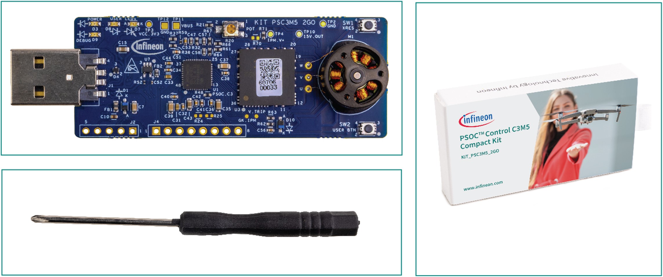
Kit contents
The KIT_PSC3M5_2GO PSOC™ Control C3M5 Compact Kit comprises the following components:
PSOC™ Control C3M5 Compact Kit
Screwdriver for potentiometer tuning
Figure 1.
Kit content
Getting Started
This guide helps you get acquainted with the evaluation kit.
The
Kit operation
section describes the major features and functionalities, such as programming, debugging, and USB-UART bridges, of the PSOC™ Control C3M5 Compact Kit
The Hardware section provides a detailed hardware description, design information, and rework details
The PSOC™ Control C3M5 Compact Kit enables the user with two operating modes; user can either run the motor in standalone mode or can connect to ModusToolbox™ Motor Suite software to control the motor operations
Application development using the PSOC™ Control C3M5 Compact Kit is supported in ModusToolbox™
ModusToolbox™ is a free development ecosystem that includes the Eclipse IDE for ModusToolbox™ PSOC™ Control C3M5 MCU. Using ModusToolbox™, you can enable and configure device resources, middleware libraries, write C/assembly source codes, and program or debug the device. For more information, see the
ModusToolbox™ software installation guide
Code examples are available for evaluating the PSOC™ Control C3M5 Compact Kit. These examples help you become familiar with the PSOC™ Control C3M5 MCU and create your own designs. These examples can be accessed through the
ModusToolbox™ Project Creator
tool. Additionally, see
Infineon code examples for ModusToolbox™ software
to access these examples
In addition to the standalone operation of the kit, ModusToolbox™ Motor Control Suite helps the user to connect with a graphical user interface to run a motor control application. Using ModusToolbox™ Motor Control Suit, the user can control the motor operations and able to see and configure motor parameters in real time using a graphical interface
For more information on the installation and operation of the ModusToolbox™ Motor Control Suite, refer to the kit operation section or the quick start guide for the kit available on the kit
webpage
Board details
The PSOC™ Control C3M5 Compact Kit has the following features:
USB-A connector for input power and system communication
XMC4200 based programmer and debugger
PSOC™ Control C3 device
Onboard BLDC motor
Infineon's Intelligent Power Module (IPM) with three-phase inverter integrated
User switch and reset switch
Potentiometer control
User LEDs
Power LED
Debug LED
Figure 2.
KIT_PSC3M5_2GO board details
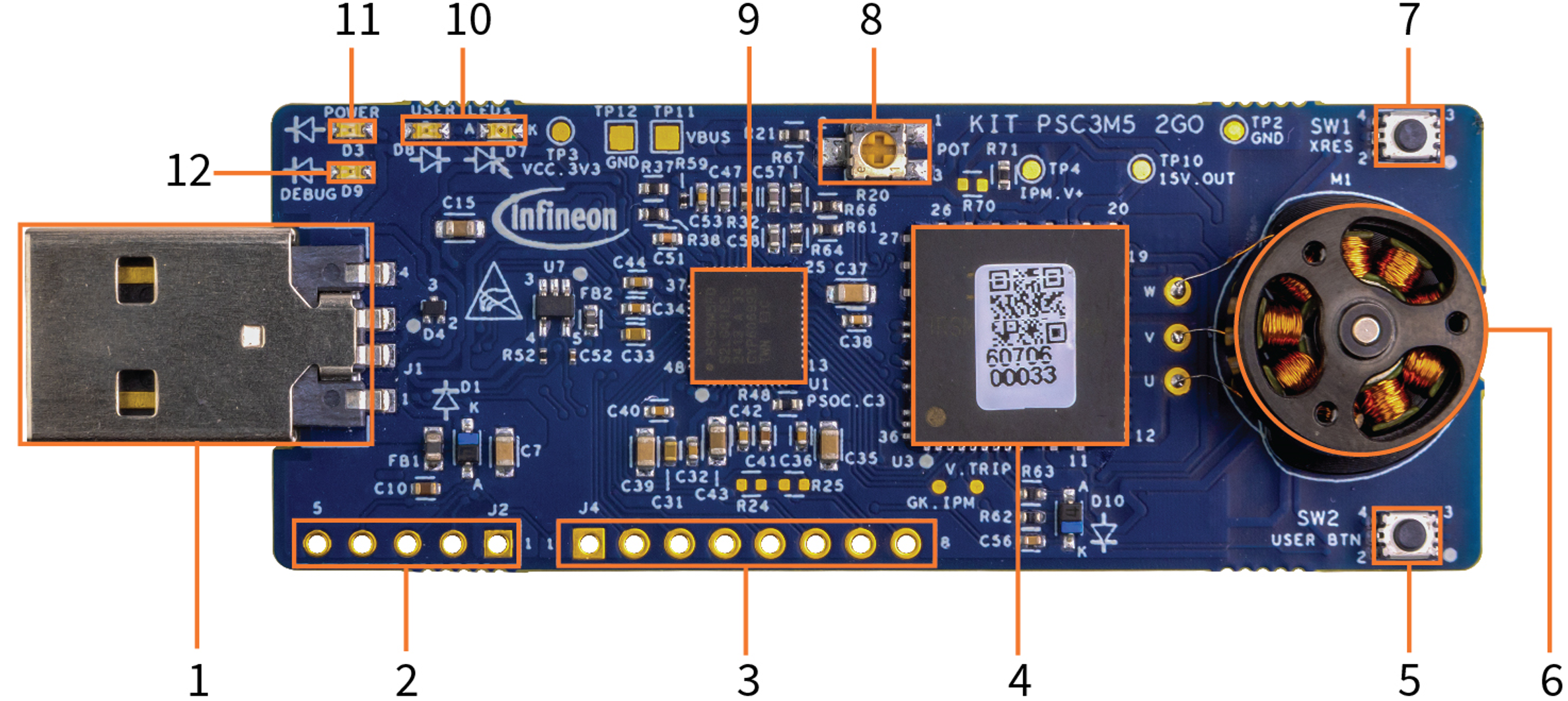
Sl No. | KIT_PSC3M5_2GO blocks |
|---|---|
1 | USB-A connector (J1) |
2 | XMC4200 SWD programming header (J2) |
3 | GPIO header option(J4) |
4 | Intelligent Power Module (IPM) three-phase (IRSM836-044MA - U3) |
5 | User button (SW2) |
6 | BLDC motor (M1) |
7 | Reset button (SW1) |
8 | Potentiometer-POT (R20) |
9 | PSOC™ Control C3 device (PSC3M5FDS2LGQ1 - U1) |
10 | User LEDs (D7, D8) |
11 | Power LED (D3) |
12 | Debug LED (D9) |
Port pin | Primary onboard function | Connection details |
|---|---|---|
P0.0 | EN_IPM | Enable signal for the IPM Module. |
P1.2 | SWDCLK | SWD clock signal. |
P1.3 | SWDIO | SWD IO signal. |
P2.0 | GK_IPM | Gate kill signal from IPM. |
P2.1 | TDO | TDO is connected to the 10-pin SWD header interface. JTAG support is not available on this board. |
P2.2 | Not connected | |
P2.3 | Not connected | |
P4.0 | PWMWL | PWM low side input to IPM. |
P4.1 | PWMVL | PWM low side input to IPM. |
P4.2 | PWMUL | PWM low side input to IPM. |
P4.3 | PWMWH | PWM high side input to IPM. |
P4.4 | PWMVH | PWM high side input to IPM. |
P4.5 | PWMUH | PWM high side input to IPM. |
P4.6 | USER_SW | User switch input. |
P4.7 | Not connected | |
P6.0 | Not connected | |
P6.1 | Not connected | |
P6.2 | Not connected | |
P6.3 | Not connected | |
P7.0 | USER_LED1 | User LED output. A RED LED (D7) is connected to this pin with the anode being connected to the VCC_3V3 supply. |
P7.1 | Not connected | |
P7.2 | Not connected | |
P8.0 | GPIO | P8.0 is connected to the J4 header. This pin supports slave select in SPI mode of operation. |
P8.1 | GPIO | P8.1 is connected to the J4 header. This pin supports MOSI in SPI mode of operation. P8.1 can be utilized as a UART RX. P8.1 can be used as an I2C clock signal by populating the R24 resistor (4.7K) for pull-up. |
P8.2 | GPIO | P8.2 is connected to the J4 header. This pin supports MISO in SPI mode of operation. P8.2 can be utilized as a UART TX P8.2 can be used as an I2C data signal by populating the R25 resistor (4.7K) for pull-up. |
P8.3 | GPIO | P8.3 is connected to the J4 header. This pin supports SPI_CLK in SPI mode of operation. |
P9.0 | USER_LED2 | P9.0 is connected to user LED—D8 (green) |
P9.2 | PSC3_UART_RX | RX from PSC3M5. TX from J-Link debugger is connected to P9.2. |
P9.3 | PSC3_UART_TX | TX from PSC3M5. RX from J-Link debugger is connected to P9.3. |
AN_A0 | IDC_LINK_PSEUDO_P | Current sense input from IPM. Motor phase current (single shunt) is sensed from AN_A0, providing feedback to the PSC3M5 device. |
AN_A1 | IDC_LINK_PSEUDO_N | Current sense input from IPM. Motor phase current (single shunt) is sensed from AN_A1, providing feedback to the PSC3M5 device. |
AN_A2 | IDC_LINK_OPAMP | Low-side single shunt current is fed to an external op-amp for gain amplification. The op-amp output is connected to PSOC™ C3 MCU device. |
AN_A3 | TEMP | AN_A3 is connected to the thermistor to monitor the temperature from the PSC3M5 device. |
AN_A4 | VDC_LINK | AN_A4 is connected to the voltage divider network to sense and monitor VDDA voltage on the hardware and to the PSC3M5 device analog supply. |
AN_A5 | Not connected | |
AN_B1 | Not connected | |
AN_B2 | AN_B2 | AN_B2 is connected to the GPIO header for external evaluation purpose. |
AN_B3 | AN_B3 | AN_B3 is connected to the GPIO header for external evaluation purpose. |
AN_B4 | M_SPEED_POT | AN_B4 is connected to the on-board potentiometer input to control the motor speed manually. |
XRES | XRES_L_MCU | Active low reset signal to PSC3M5 device. The reset switch is used to manually reset the MCU. |
Motor details
No. | Item | Requirement | Note |
|---|---|---|---|
1 | Rated voltage (V) | 6.5 | |
2 | No-load current (A/6.5 V) | ≤0.1 | Final inspection item, current tester |
3 | No-load speed (RPM/6.5 V) | 20850±5% | Final inspection item, speed tester |
4 | Motor internal resistance (Ω)(Environmental temperature: 25℃) | 12±1 | Final inspection item, DC low resistance selector |
5 | Whole machine weight (g) | ≤5.5 | Final inspection item, electronic balance (sampling) |
6 | Machine insulation/leakage current | DC 200 V(3 s)/3 mA | Final inspection item, high voltage tester |
7 | Machine balance (mg) | ≤5 | Production inspection item, dynamic balance (sampling) |
8 | Operating environment temperature (℃) | -10℃-65℃ | |
9 | Storage temperature (℃) | -10℃-50℃ | |
10 | Storage humidity (%) | ≤85 |
No. | Item | Requirement | Note |
|---|---|---|---|
1 | Slot number | 9N8P | |
2 | Whole machine outline (mm) | ≤1.0 | Final inspection item, ruler |
3 | Whole machine height (mm) | 8.8±0.1 | Final inspection item, ruler (sampling) |
4 | End play (mm) | ≤0.05 | Production inspection item, thousandth inspection (sampling) |
5 | Radial play (mm) | ≤0.05 | Production inspection item, thousandth inspection (sampling) |
6 | Motor height (mm) | 7.9±0.1 | Final inspection item, ruler (sampling) |
7 | Whole machine outer diameter (mm) | 13.6±0.1 | Final inspection item, ruler (sampling) |
8 | Installation hole position (mm) | 5.84 11.68 3-M1.2 | Final inspection item, ruler (sampling) |
9 | Wire/wire sequence | Painted wire, same color | Final inspection item, visual inspection |
10 | Line length (mm) | 8~9 mm | Final inspection item, ruler (sampling) |
Technical support
For assistance or product related queries, contact
Infineon Support
or post your queries on the
Infineon Developer Community
platform.
Abbreviations and definitions
Abbreviation | Definition |
|---|---|
USB | Universal serial bus |
PSOC | Programmable system on chip |
CPU | Central processing unit |
FOC | Field-oriented control |
MCU | Micro controller unit |
ADC | Analog-to-digital converter |
BLDC | Brush-less direct current |
SWD | Serial wire debug |
JTAG | Joint test action group |
PCB | Printed circuit board |
PWM | Pulse width modulation |
PMSM | Permanent magnet synchronous motor |
GPIO | General purpose input/output |
I2C | Inter-integrated circuit |
UART | Universal asynchronous receiver transmitter |
SPI | Serial peripheral interface |
CORDIC | Coordinate rotation digital computer |
IPM | Intelligent power module |
Op-amp | Operational amplifier |
Kit operation
Out-of-box: Standalone operation
The kit is pre-programmed with the out-of-box (OOB) firmware, which is configured to operate the included motor in sensorless field-oriented control (FOC) single-shunt mode.
Connect the PSOC™ Control C3M5 Compact Kit to a 5 V USB-A power adapter or computer USB socket. The green power LED (D3) and green debug LED (D9) will turn on
The onboard motor starts spinning in the clockwise direction (from the motor’s front side). The motor speed is controlled by the potentiometer (R20)
Rotate the potentiometer to adjust the motor speed
During sensorless close-loop operation, motor stops if the set speed is too low due to brake boot mode of motor state machine
To restart the motor, set the speed to ‘0’ and then increase it again using the potentiometer
The user button (SW2) changes the motor's direction. In the closed loop, when SW2 is pressed, the motor speed ramps down to ‘0’ and stops. Set the potentiometer (R20) speed to ‘0’ and then increase the speed to restart the motor in the reverse direction. In case of open loop (when motor speed is too low <20%), it automatically spins in reverse direction upon switch press
The green user LED (D8) shows the motor's direction:
Off - Clockwise direction
On - Counter-clockwise direction
Note:
The motor speed is determined by the potentiometer setting. If the potentiometer is set to ‘0’ (fully turned counterclockwise), the motor will not run.
Note:
Due to inherent variations in motor mechanical tolerances, some level of noise is expected from the board while the motor is spinning. The noise level may vary between boards. From a measurement perspective, the actual noise remains below 63 dB for all boards.
OOB: GUI-based operation
Download and install ModusToolbox™ Motor Suite Setup for Windows from the Infineon Developer Center or use the link
ModusToolbox™ Motor Suite
(minimum required version: 2.4.1)
Connect the compact kit to the PC via USB-A connector and then open the ModusToolbox™ Motor Suite GUI
Figure 3.
GUI: Open new project
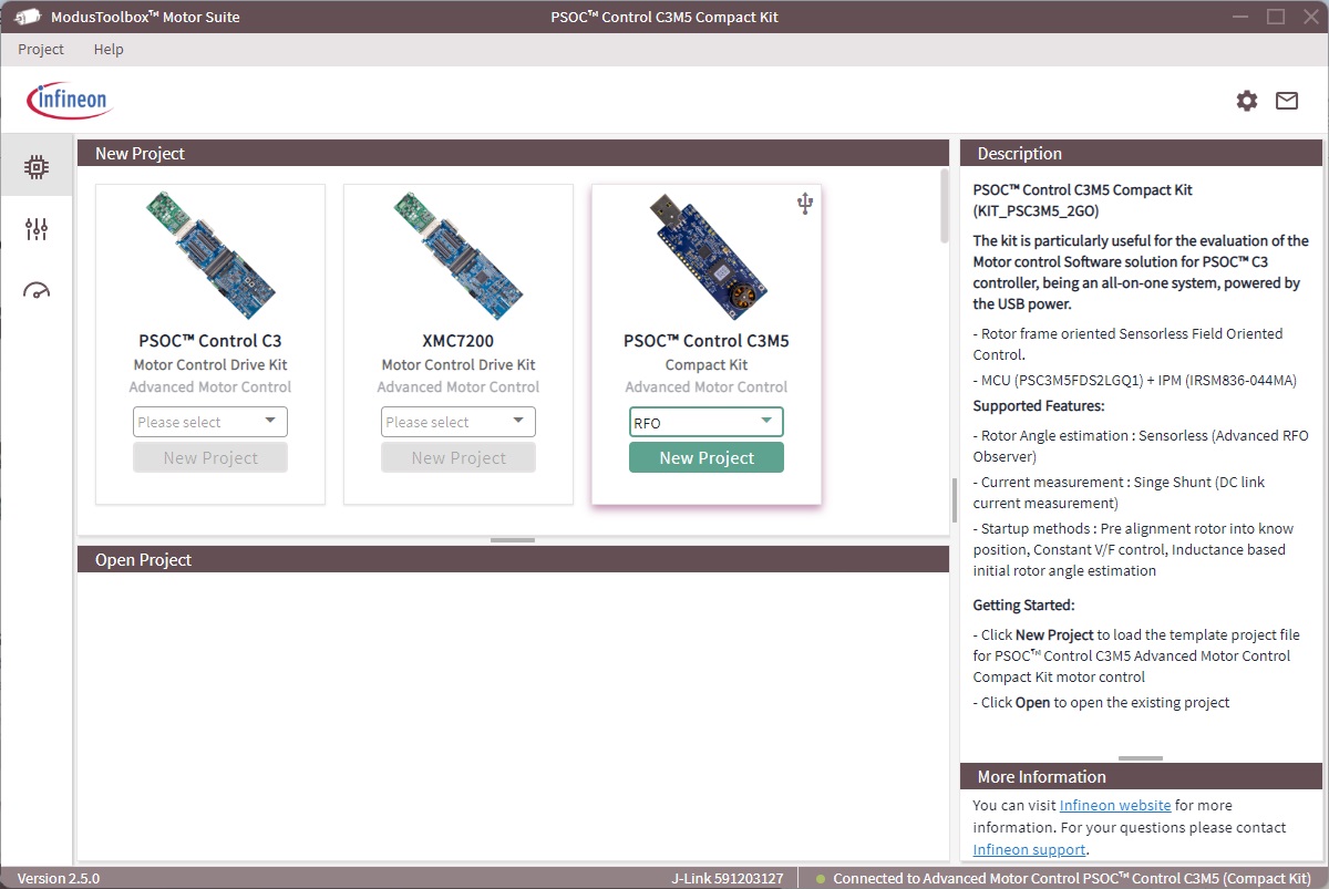
Go to PSOC™ Control C3M5 Compact Kit , select RFO , and click New Project to open the configurator view
Figure 4.
GUI: Configurator view
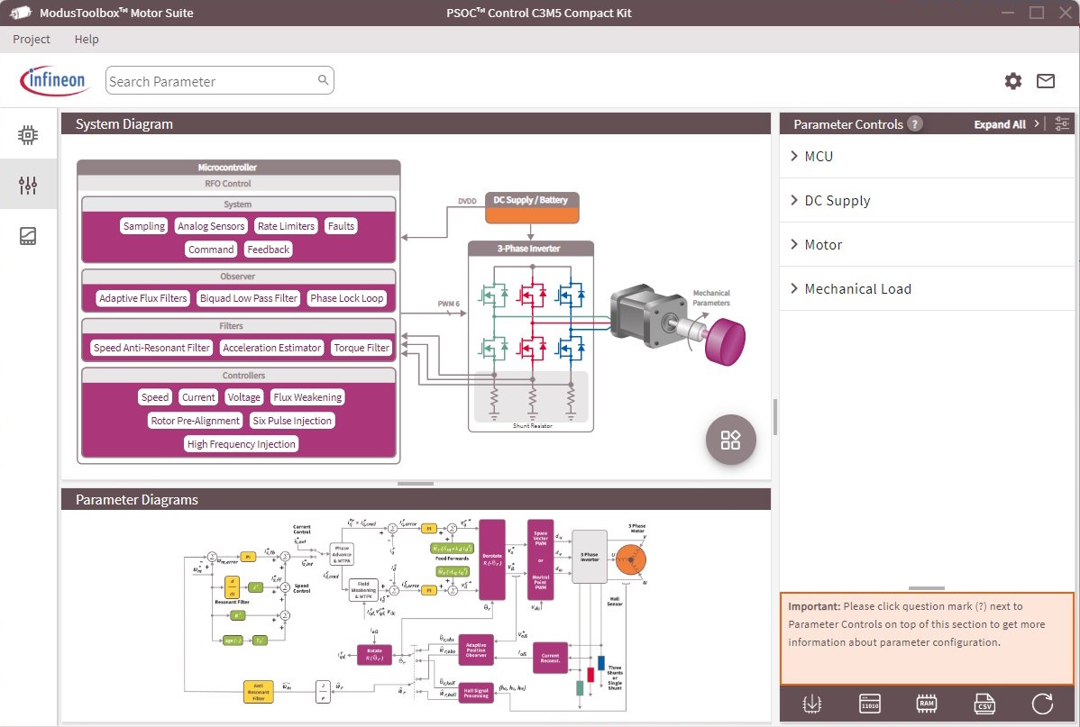
A green dot at the bottom right of the GUI windows indicates a successful connection to the kit. The configurator view provides the option to configure the static parameters
Click Flash Firmware on the lower right side and then click on the Default option to reprogram the default firmware into the controller
Click the Test Bench button to switch to the Test Bench view
Figure 5.
GUI: Test Bench view
In the Command Panel , the drive switch is used to enable/disable the drive
If the Potentiometer Control switch is on, then the potentiometer (R20) on the kit controls the motor speed
To set the motor speed using the Target Set slider in the Command Panel , turn the Potentiometer Control switch in the GUI
Note:Emergency stop under the Faults tab is used to stop/restart the motor and clear the faults
The Control Panel and Command Panel sections display parameters such as voltage applied, currents flowing, DC bus voltage, faults, control scheme, state of the state machine, and the motor direction
To view current waveforms or other parameters, launch the Oscilloscope by clicking the icon in the top right corner of the Motor Suite GUI. For further details, refer to the user manual in the top corner inside the Oscilloscope window
Note:
During the installation process, if prompted to install the J-Link driver, select "Yes" if it is not already installed on the test PC.
Figure 6.
Oscilloscope view
Oscilloscope view can be used to visualize any global variable in the project. It allows up to 4 variables to be monitored simultaneously.
Figure 6
shows the three motor phase currents reconstructed from single shunt DC link current measurements.
Creating project and programming/debugging using ModusToolbox™
The PSOC™ Control C3M5 Compact Kit can be programmed and debugged using the onboard J-Link debugger. This onboard programmer/debugger supports USB-UART bridge functionality. An XMC4200 device is used to implement the J-Link functionality. See UM08001: J-Link/J-Trace Getting started document in
J-Link downloads
for more details.
The following steps briefly introduce project creation, programming, and debugging using ModusToolbox™. For detailed instructions, see the
Eclipse IDE for ModusToolbox™ user guide
.
Connect the KIT_PSC3M5_2GO Compact Kit to the PC via USB-A connector, as shown in
Figure 7
. It enumerates as a USB composite device if you are connecting it to your PC for the first time
Figure 7.
Connect compact kit to PC via USB-A connector
The debugger on this kit features the J-Link LITE with UART. The debug LED (green) is always ON if the USB is connected
In the Eclipse IDE for ModusToolbox™, import the desired code example (application) into a new workspace
Click New Application on the Quick Panel tab
Figure 8.
Create new application
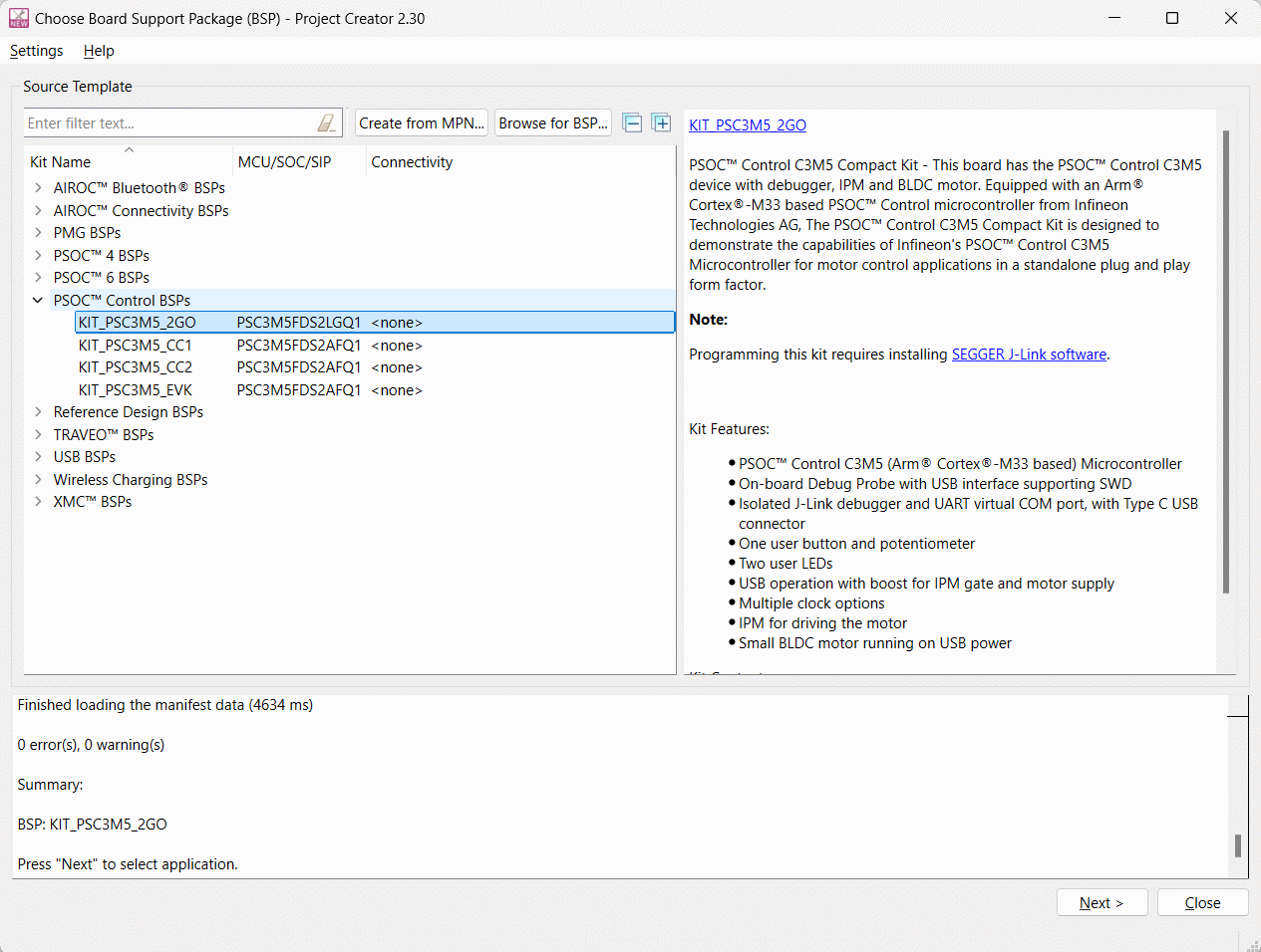
Select BSP -KIT_PSC3M5_2GO in the Choose Board Support Package window and click Next
Figure 9.
Choose Board Support Package
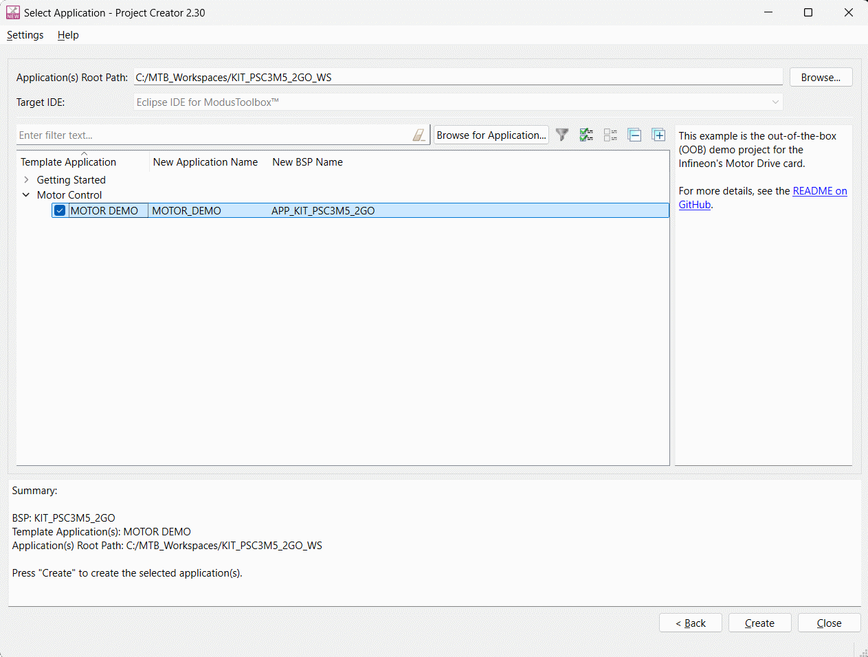
Select the application in the Select Application window and click Create
Figure 10.
Select application
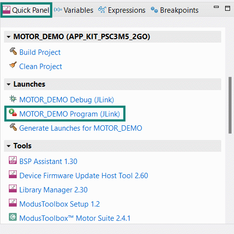
To build and program a PSOC™ Control C3M5 MCU application, follow these steps:
In the Project Explorer tab, select <App_Name> project
In the Quick Panel tab, scroll to the Launches section and click the <App_Name> Program (J-Link) configuration
Figure 11.
Programming in ModusToolbox™
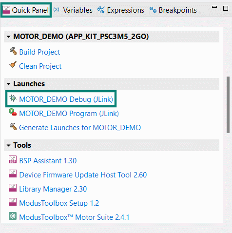
ModusToolbox™ has an integrated debugger. To debug a PSOC™ Control C3M5 MCU application, follow these steps:
In the Project Explorer tab, select <App_Name> project
In the Quick Panel tab, scroll to the Launches section and click the
<App_Name> Debug
(J-Link) configuration
Figure 12.
Debugging in ModusToolbox™
For a detailed explanation on how to debug using ModusToolbox™, see the 'Program and debug' section in the
Eclipse IDE for ModusToolbox™ user guide
.
Hardware
The hardware section provides details about the design document and how every block in the hardware is designed.
This section details each schematic block in the design. The user may have to rework the hardware in a few of the cases where provisions are given but components on the board are not populated by default.
Rework instructions are given in this section, and for any component manufacturer part number, refer to the kit PCBA bill of materials on the kit
webpage
.
Schematics
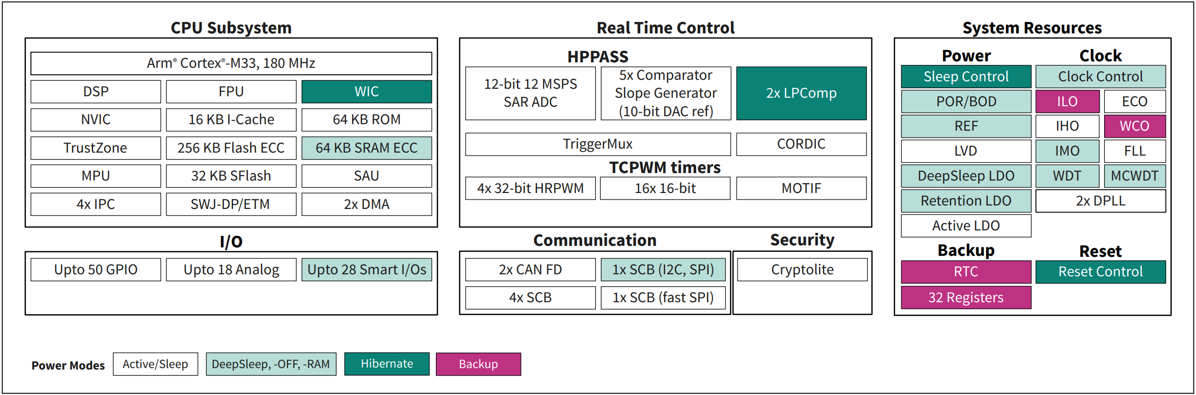
The PSOC™ Control C3M5 Compact Kit is built around the PSC3M5 MCU. The following section describes the block diagram of the PSC3 device and peripherals on the board. For more information on device features, see the
device datasheet
.
Figure 13.
PSOC™ Control C3M5 device block diagram
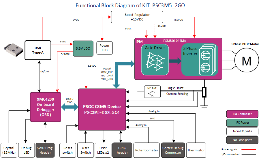
KIT_PSC3M5_2GO block diagram
shows the power supply connections, peripheral interface, and motor connections on the kit.
Figure 14.
Functional block diagram
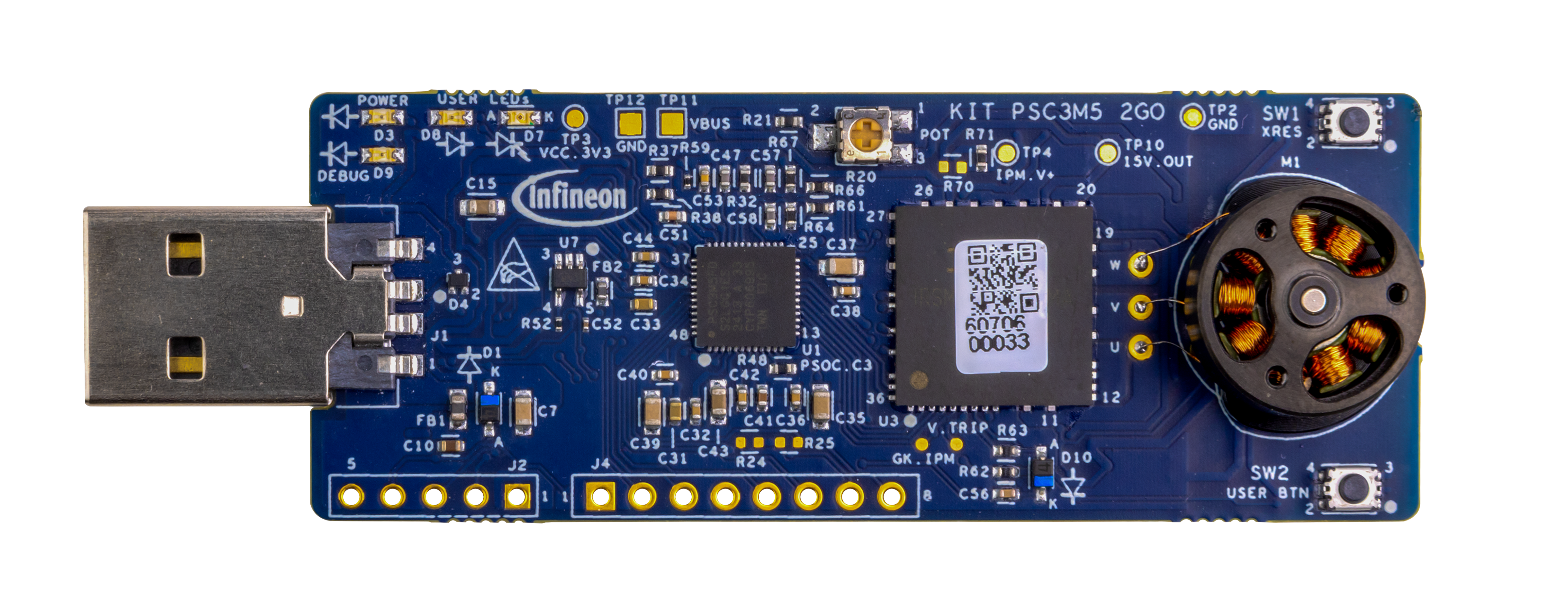
KIT_PSC3M5_2GO image
Figure 15.
KIT_PSCM5_2GO board top view
Hardware functional description
The PSOC™ Control C3M5 Compact Kit is designed as a plug-and-play device to demonstrate motor spinning applications. The kit is supported in ModusToolbox™ for comprehensive development purposes. With an intuitive graphical user interface, users can effortlessly adjust motor speed and direction in real-time, utilizing PWM control within the application. This user-friendly interface simplifies the development process, allowing designers to focus on creating innovative motor control solutions.
PSOC™ C3M5 MCU (PSC3M5FDS2LGQ1)
PSC3M5FDS2LGQ1 is a PSOC™ C3 family of devices with industrial power and motor applications. The PSC3P5xD and PSC3M5xD devices are based on the Arm® Cortex®-M33 running up to 180 MHz with DSP and FPU capability. In addition to the CPU subsystem, the devices contain advanced real-time control peripherals, such as a high-performance programmable analog subsystem, comparators, advanced timers with high-resolution capability, up to six SCBs, and two CAN FDs for communication. The devices support one active and five low-power modes for managing and reducing power consumption, depending on application requirements.
Figure 16.
PSOC™ Control C3M5 device design
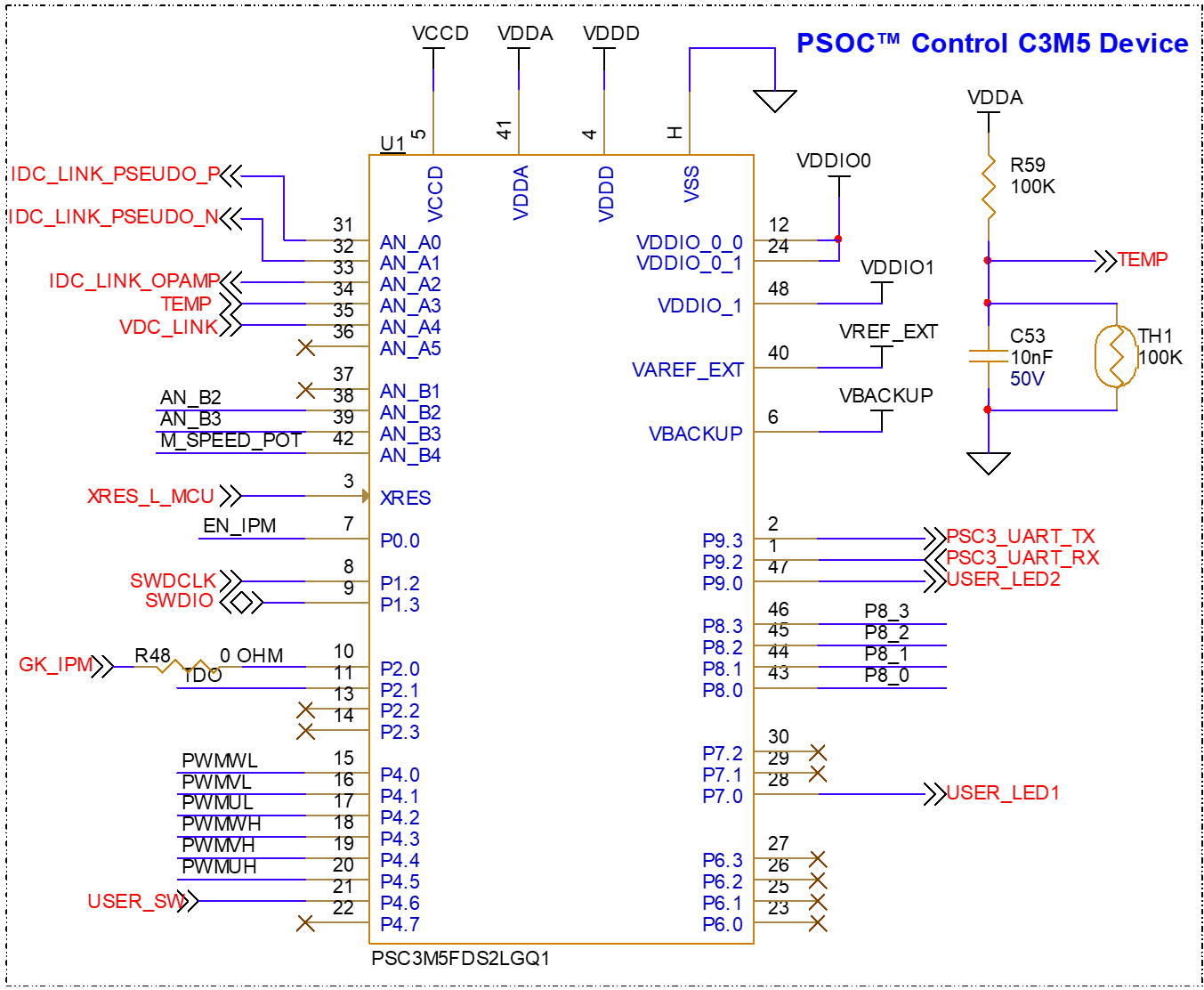
Figure 17.
PSOC™ Control C3M5 device power
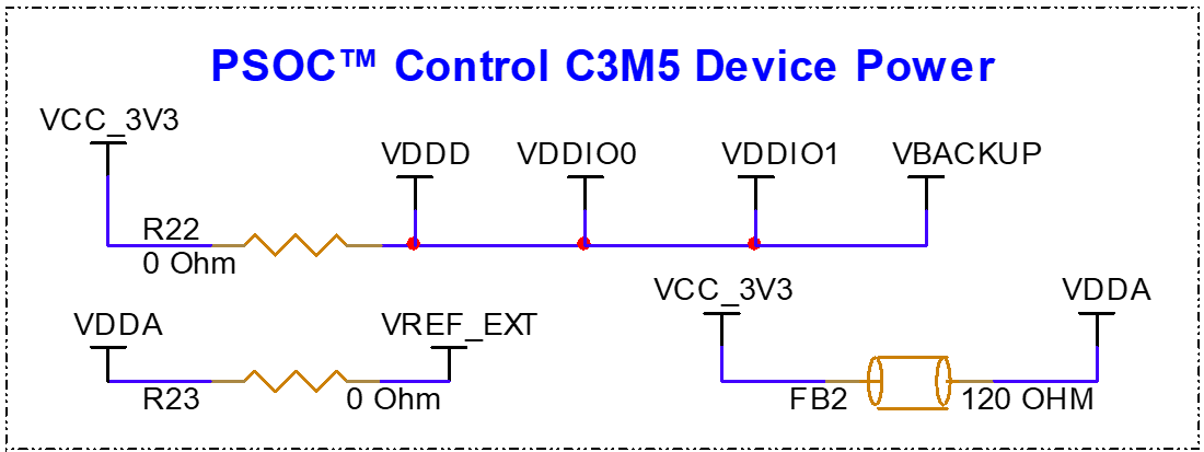
Figure 18.
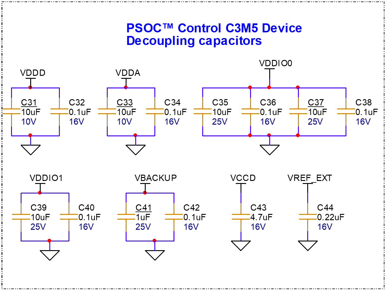
PSOC™ Control C3M5 device decoupling capacitors
XMC4200 based on-board programmer/debugger
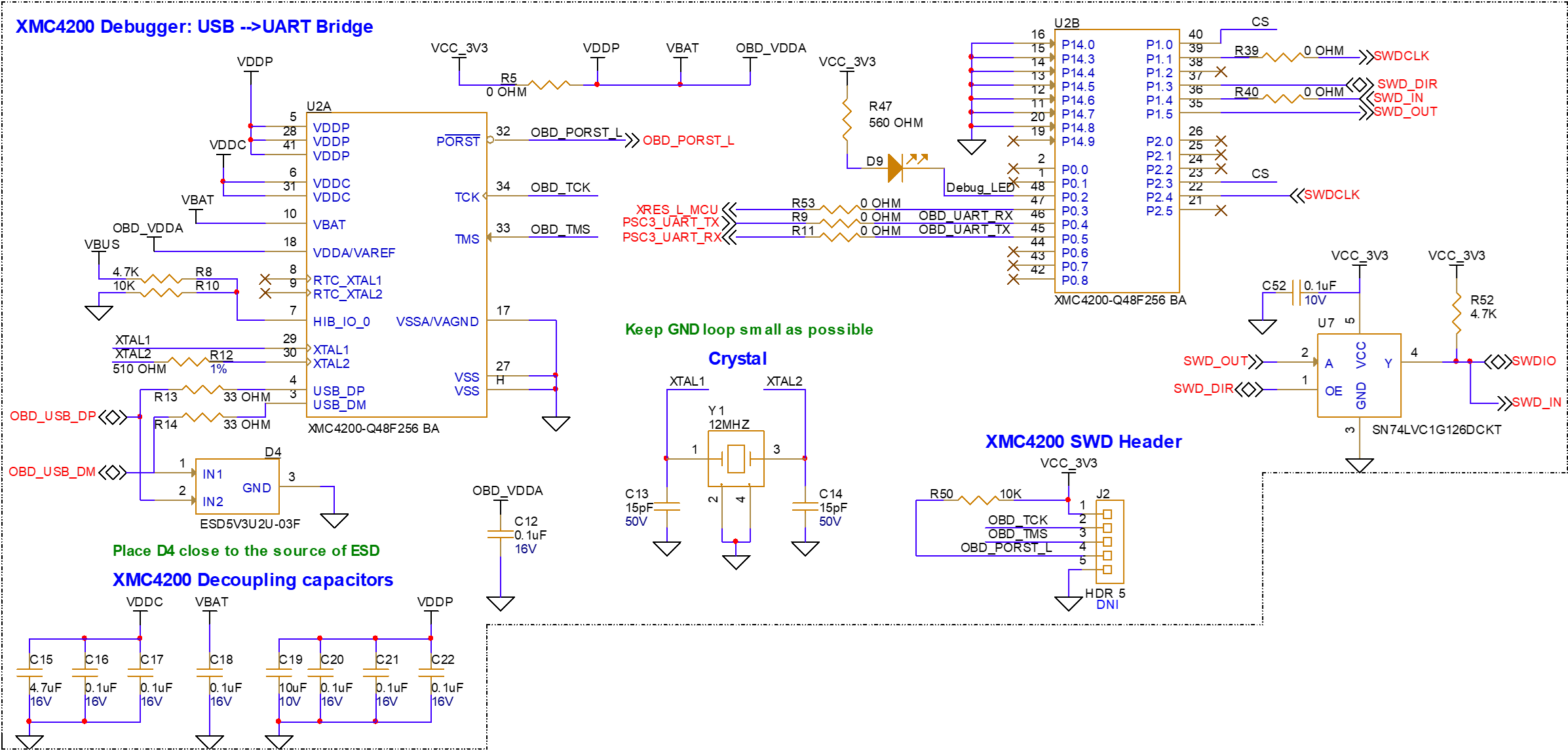
XMC4200 is a member of the XMC4000 family, which incorporates a bridge between the USB interface and the PSOC™ Control C3M5 device. XMC4200 is a J-Link programmer and debugger on the board. The USB-SWD and USB-UART interfaces help the user to interact with the hardware by establishing communication between the target device and the test systems while programming and debugging. XMC4200 is preloaded with application-specific firmware to support SWD and UART communications on the kit.
Figure 19.
XMC4200 on-board debugger
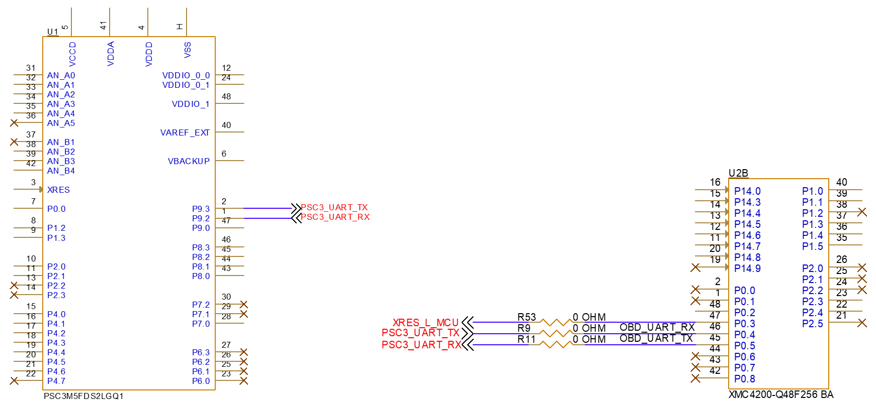
Serial interconnection between XMC4200 and PSOC™ C3M5 MCU
The XMC4200 device works as a USB-UART bridge on the board, providing UART communication between the target MCU and the test PC.
Figure 20.
UART interface between XMC4200 and PSC3M5 device
Power supply system
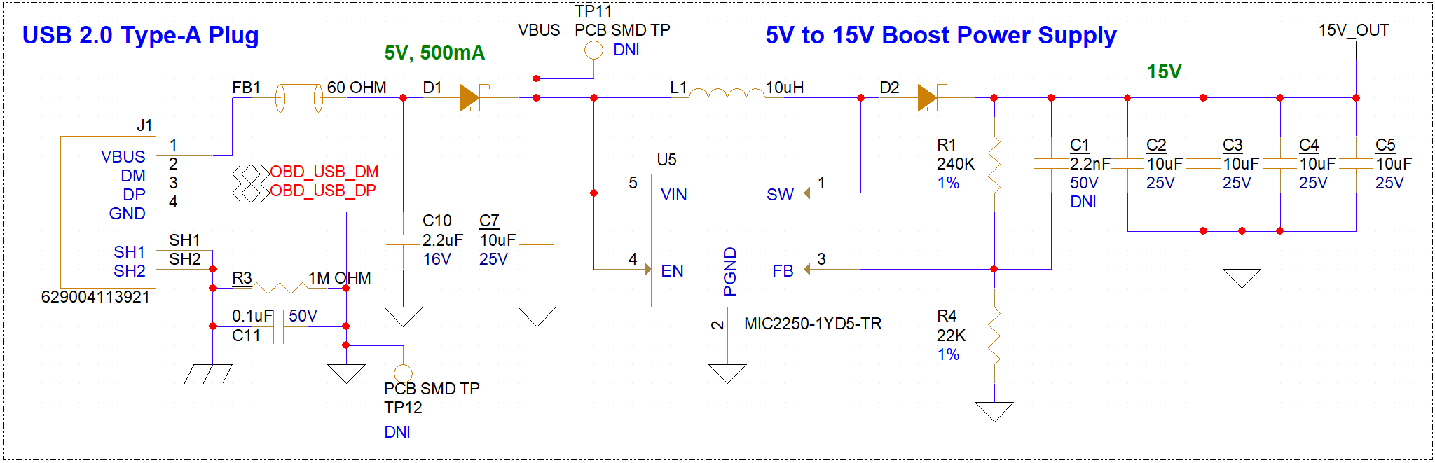
External power through USB is the source of power on the kit. There are two fixed power rails running on the board.
A fixed 3.3 V will be generated from a linear voltage regulator, which uses VBUS (USB-5 V) as input and generates a 3.3 V output for PSOC™ Control C3 device, XMC4200 debugger, and other peripherals.
A boost regulator is used on the kit to generate 15 V output from a 5 V USB input. The IPM module inverter circuitry requires 15 V input to operate.
Voltage regulators and reverse voltage protection
The linear regulator TLS208D1EJV33XUMA1 from Infineon is designed to generate a fixed 3.3 V output from VBUS. This LDO has internal protection for overcurrent (>800 mA), short circuit protection, and an overtemperature protection feature.
An adjustable boost switching regulator MIC2250-1YD5-TR is used on the kit, generating the 15 V output required for IPM inverter circuitry. The regulator must have a built-in soft start to avoid any inrush and prevent output voltage overshoot.
TVS diodes are included at the output of both USB and the boost regulator circuit to prevent any kind of damage to the input/source supply from reverse supply of voltage.
Figure 21.
3.3V LDO
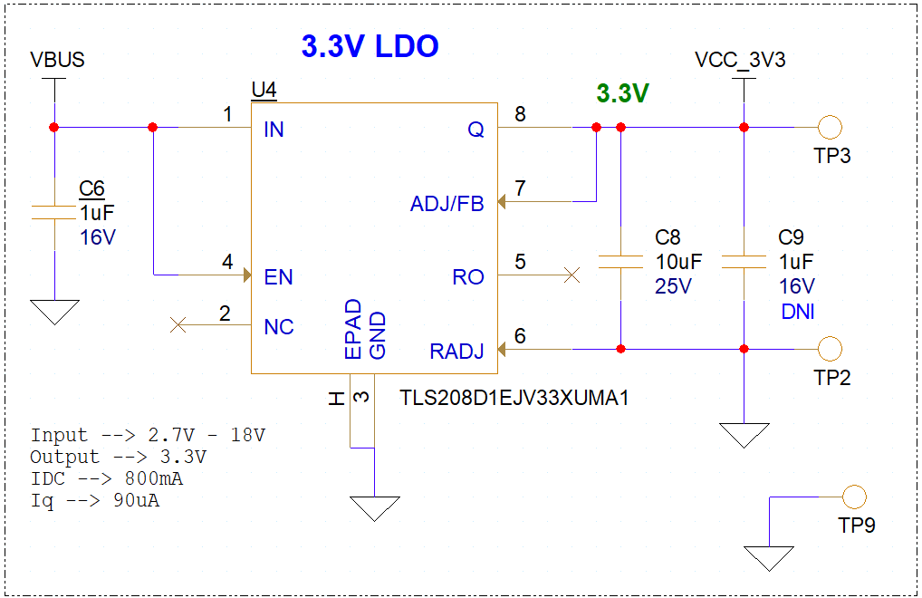
Figure 22.
VBUS supply and 15V boost regulator
I/O headers
A GPIO header on the kit allows the user to use interfaces such as UART, I2C, or SPI from external boards or sensors.
Provision is given to populate an 8-pin header from which the user will be able to communicate from the PSOC™ Control C3M5 device to any externally connected device or sensor interface. The default configuration does not populate connector J4, so the user needs to populate it themselves. For connector details, refer to the PCBA BOM for the kit available on the kit
webpage
.
The connector J4 has a provision to communicate with external devices or sensors using the I2C, UART, or SPI interface.
Table 7
provides the pin assignment for the specific communication interface. In case of using I2C communication, while there are no pull-up options available in the external interface connected, the user needs to have pull-up resistors (R24 and R25) populated on the board.
Figure 23.
GPIO header
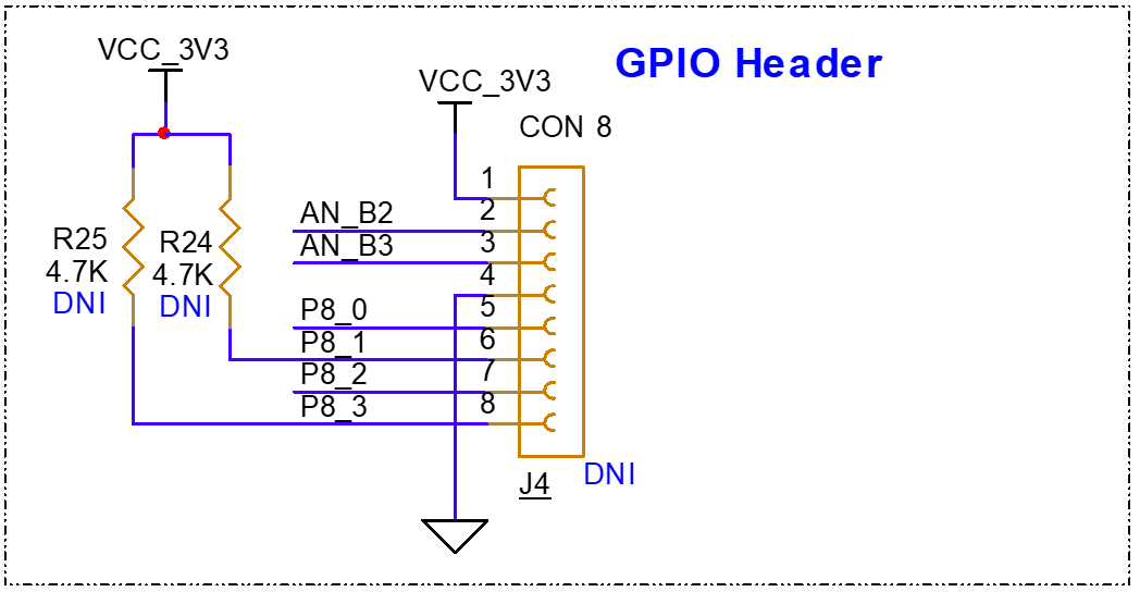
Pin | I2C | UART | SPI |
|---|---|---|---|
P8.0 | CS | ||
P8.1 | SCL | RX | MOSI |
P8.2 | MISO | ||
P8.3 | SDA | TX | CLK |
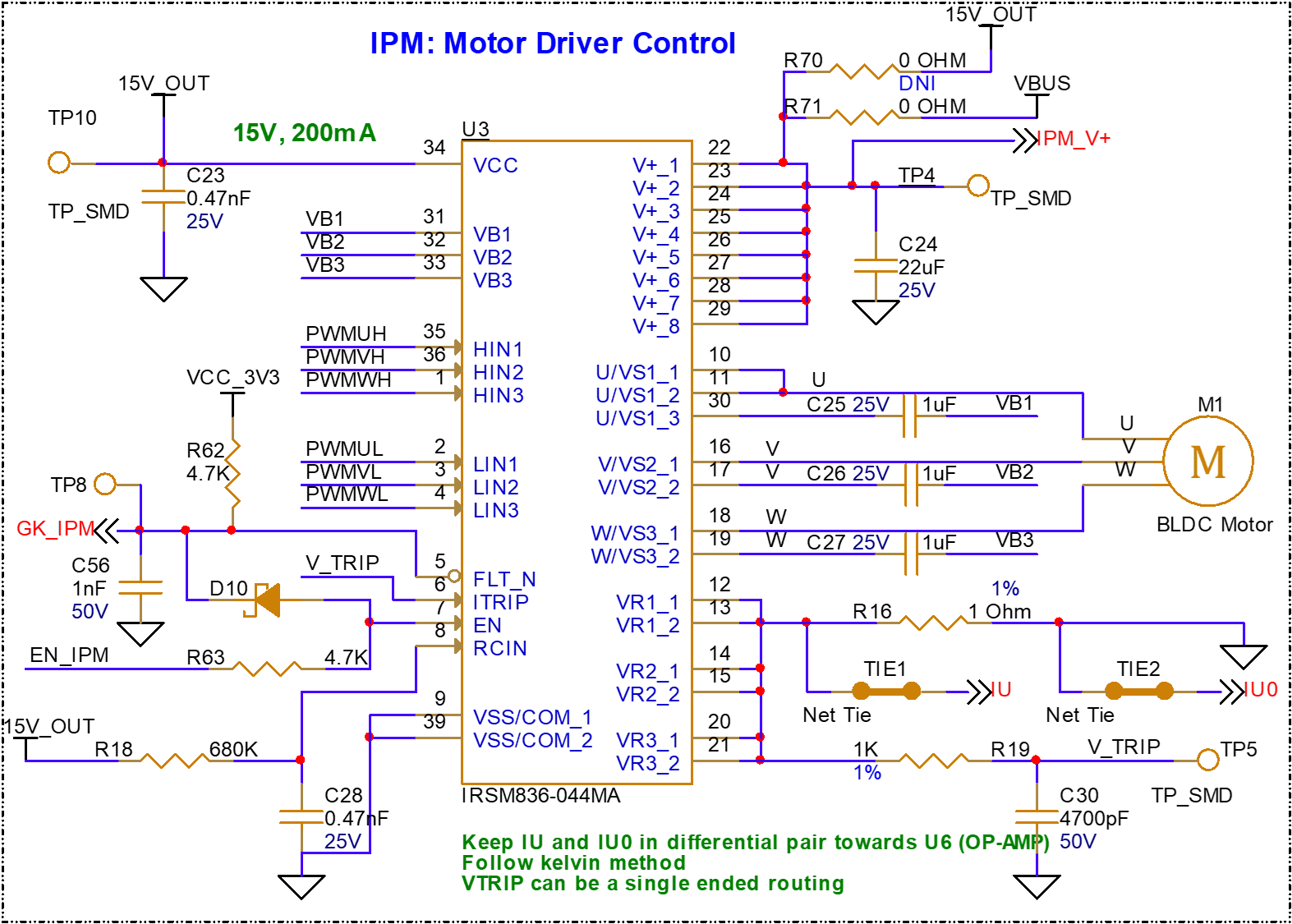
IPM motor driver module operation
Intelligent Power Module IRSM83044 device is used on the board as an integrated power module for motor control applications. IPM is integrated with inverter circuitry and the gate drivers for motor control applications.
Figure 24.
Intelligent Power Module (IPM)
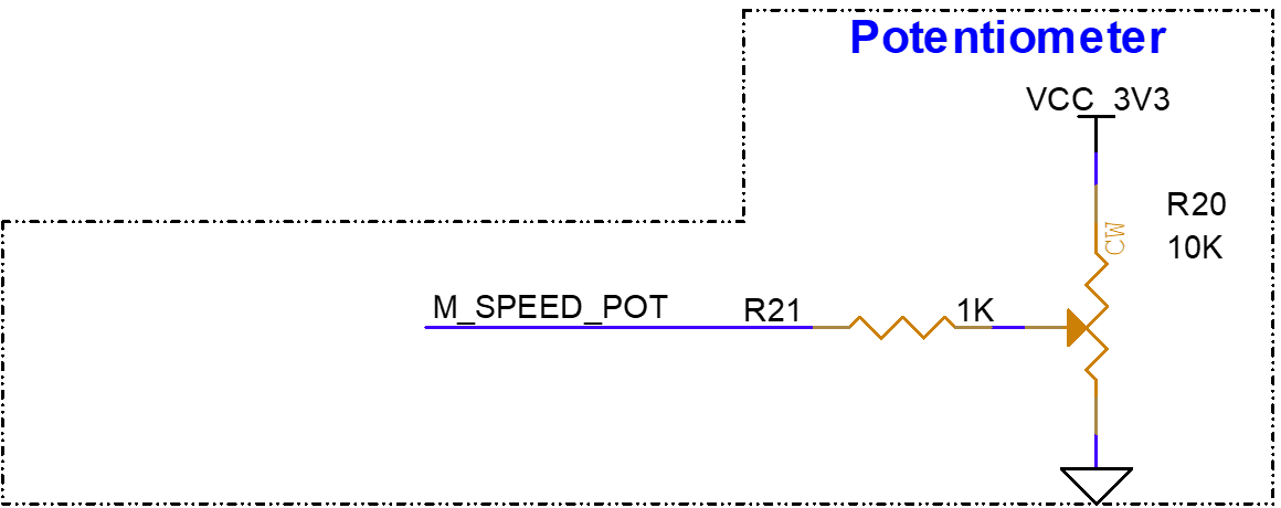
Potentiometer
A potentiometer is used for speed control applications. The PSOC™ C3 device will be used to control the speed of the motor based on potentiometer input in standalone application. Speed control can also be controlled from the ModusToolbox™ Motor Suite application.
Note:
Do not overstress the potentiometer while adjusting the motor speed. Over force applied on rotary control of potentiometer may cause permanent damage to the component.
Figure 25.
Potentiometer
LEDs
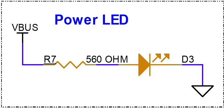
Power LED
The Power LED will glow once the board is powered using USB. LED is connected to the VBUS supply of the USB input.
Figure 26.
Power LED
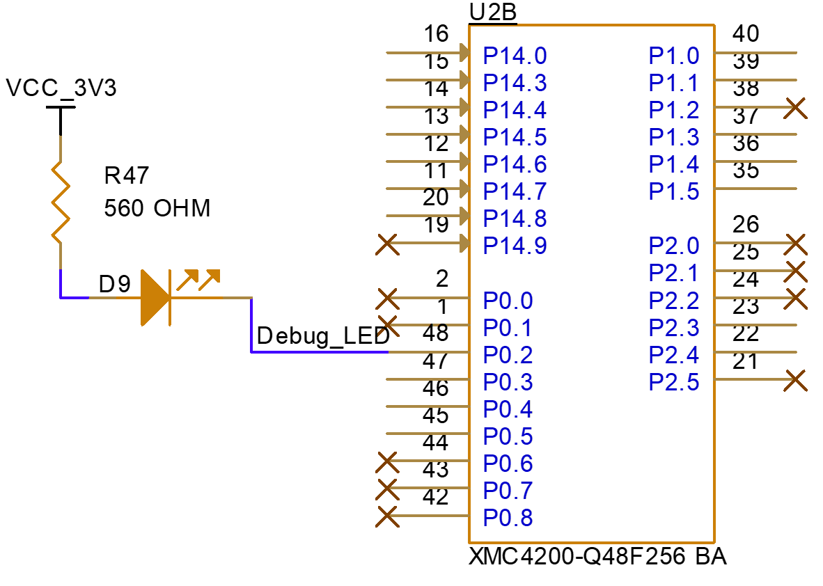
Debug LED
An LED connected to the XMC4200 to denote debug status: whenever the user undergoes debug mode and transmits or receives any data from the USB bridge using SWD, LED D9 will show the status by blinking based on live communication.
Figure 27.
Debug LED
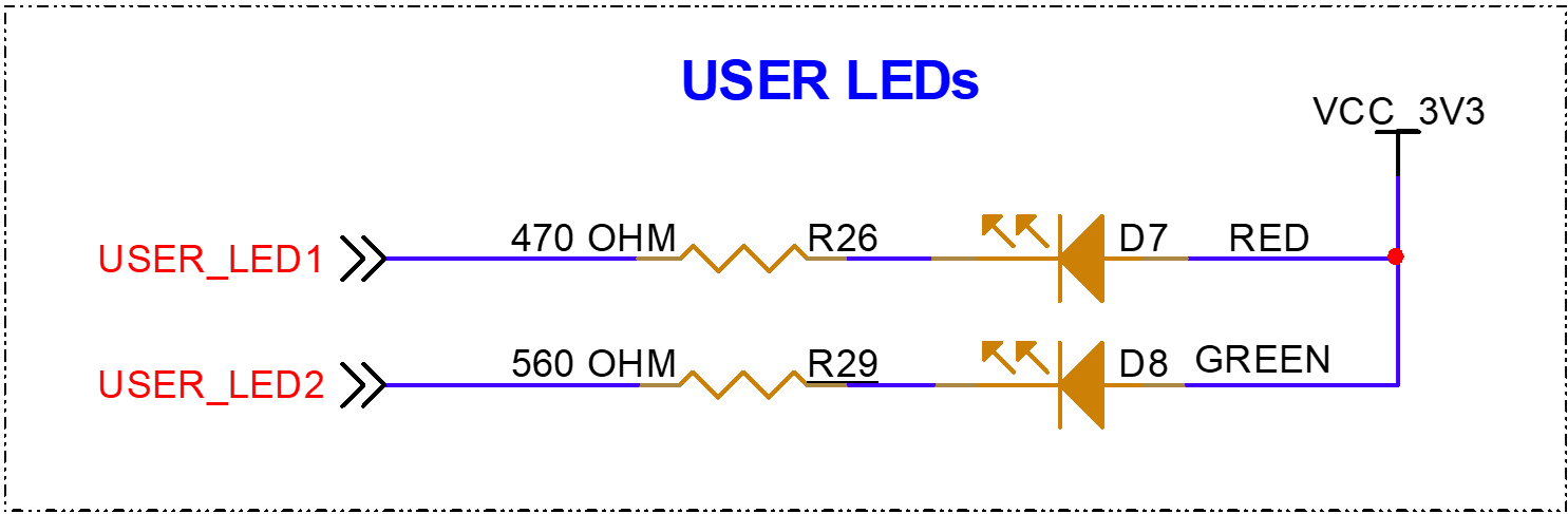
User LEDs
The compact kit will have two user LEDs connected to free IOs. The user can utilize these LEDs for any indication purpose based on the user-specific application.
Figure 28.
User LEDs
Reset and user buttons
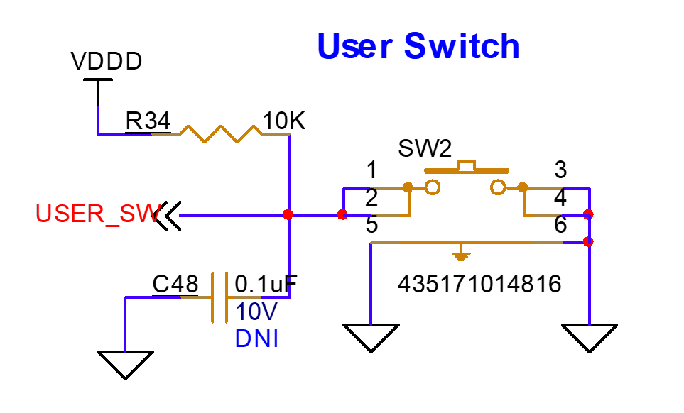
User button
The user button (SW2) is provided for user application purpose. P4.6 from the PSOC™ C3 device is connected to SW2. Default program loaded on the kit shall use SW2 for direction control of the motor while operating in standalone mode. Upon pressing SW2 motor changes its direction from clockwise to counter clock wise direction and vise versa. A LED indication is provided for per-programmed application which denotes direction of the motor based on SW2 control.
Figure 29.
User switch
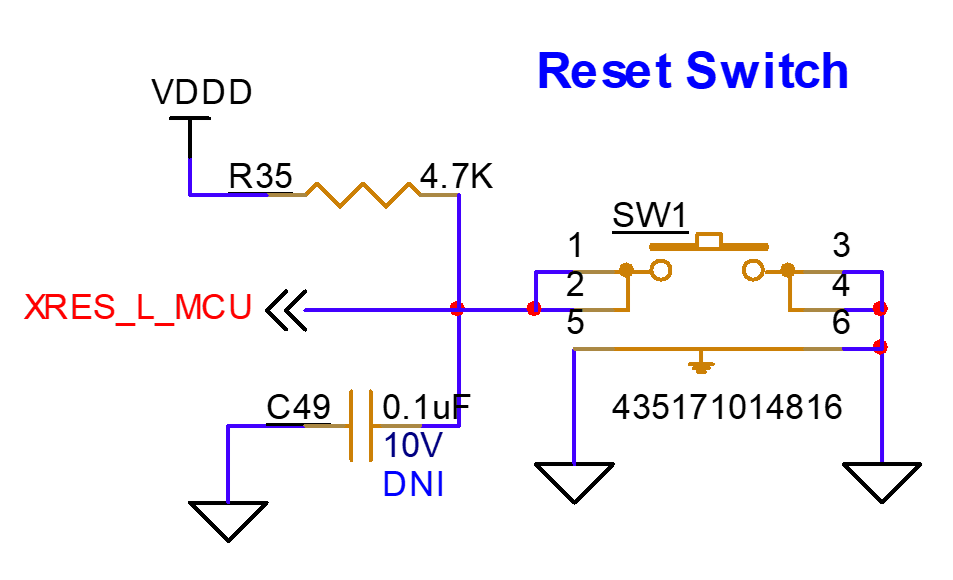
Reset switch
A hardware reset can be obtained from the reset switch. The PSOC™ C3 MCU must reset upon pressing this switch. Motor Suit application would break the connectivity from the board upon pressing SW1. Motor shall still continue to run in standalone mode. User required to reconnect the hardware to operate from motor suit GUI application.
Figure 30.
Reset switch
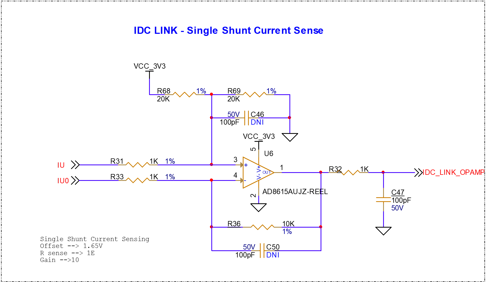
OP_AMP for single shunt FOC
Single Shunt FOC Operation
Motor control application on this kit is based on a low-side single shunt current sensing method. A 1 Ω shunt resistor is connected on the LOW side FET of the IPM module. All three phases are tied to a single shunt resistor, and it operates in single shunt FOC mode. As a current sensing operation, an external op-amp is used to get appropriate gain on the PSOC™ Control C3 device. The output of the op-amp (IDC_LINK) is given to the PSOC™ Control C3 device ADC for further processing and motor control applications.
Figure 31.
Single Shunt FOC using external op-amp
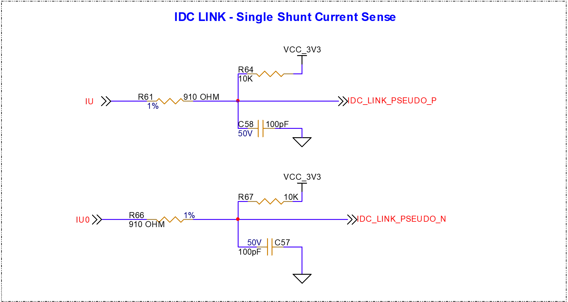
Pseudo differential mode
Apart from the external op-amp, provision is given on the board for the pseudo differential mode of operation, which will isolate the op-amp circuitry. The shunt measurement is directly given to the two different ports of the PSOC™ control C3 device. Two ADC signals must be processed further for internal gain control and current sensing applications for motor control operation.
Figure 32.
Single shunt FOC using pseudo differential method
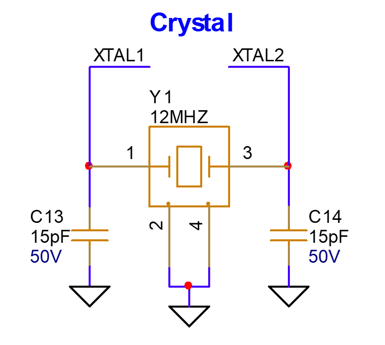
Crystal oscillators
A 12 MHz crystal is used as an external clock source for the XMC4200 on-board debugger. The XTAL1 and XTAL2 pins of the XMC4200 are connected to the external crystal operation.
Figure 33.
Crystal for XMC4200 on-board debugger
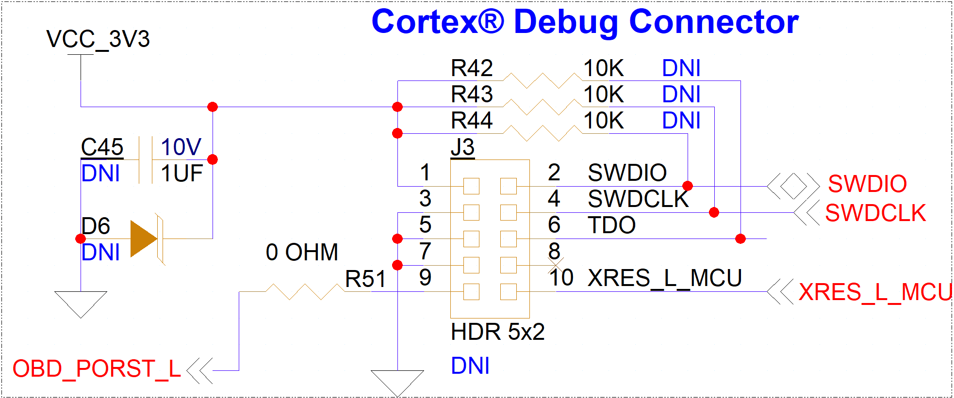
PSOC™ C3M5 MCU 10-pin SWD header (Cortex® debug header)
Provision for a 10-pin Cortex® standard debug connector is given on the board (only a footprint). External debuggers such as Segger J-Link can be connected to the header for debug and programming purposes. Only the SWD interface is enabled on the board. The JTAG function is not supported on the board.
Figure 34.
Cortex® debug connector
PSOC™ C3M5 Board rework
The PSOC™ Control C3M5 Compact Kit has the majority of the components assembled on the board for a specific functionality. In a few cases where the component is not loaded on the board (only the footprint is available), the user needs to have particular rework done on the board based on the requirement. Based on the reference designator defined in the schematic design, the user can populate the required component on the board. For manufacturer details of the component, refer to the PCBA bill of material available for the kit on the
webpage
.
Rework on 10-pin SWD connector
10-pin Cortex® debug connector rework
To connect external debuggers to the board, KIT_PSC3M5_2GO need to be assembled with 10-pin connector (J3) suitable with the footprint provisioned.
Preferred part: FTSH-105-01-L-DV-K
User is expected to assemble discrete components to enable the hardware, such as resistors R42, R43, and R44 also input bypass capacitor C45 and diode D6 to avoid damage from voltage surges causing from external emulators.
Figure 35.
Rework details for Cortex® debug connector

Bill of Materials
Refer to the Printed Circuit Board Assembly Bill of Materials (PCBA BOM) file available on the kit
webpage
Revision history
Document revision | Date of release | Description of changes |
|---|---|---|
** | 2025-04-28 | Initial release |
*A | 2025-07-25 | Updated Board details Updated Out-of-box: Standalone operation |
Trademarks
PSOC™, formerly known as PSoC™, is a trademark of Infineon Technologies. Any references to PSoC™ in this document or others shall be deemed to refer to PSOC™.