KIT_PSC3M5_DP1 PSOC™ Control C3M5 Complete System Dual Buck Evaluation Kit user guide
About this document
Scope and purpose
This document describes the features and hardware details of the Dual Buck Evaluation Board. It is designed to provide an evaluation platform for digital control applications with the
PSOC™
Arm® Cortex®-M33 based MCU. This board is part of Infineon’s digital power evaluation platform kits.
Intended audience
This document is intended for KIT_PSC3M5_DP1 users, and this board is intended to be used under laboratory conditions.
Important notice
“Evaluation Boards and Reference Boards” shall mean
products embedded on a printed circuit board (PCB) for demonstration and/or
evaluation purposes, which include, without limitation, demonstration, reference
and evaluation boards, kits and design (collectively referred to as “Reference
Board”).
Environmental conditions have been considered in
the design of the Evaluation Boards and Reference Boards provided by Infineon
Technologies. The design of the Evaluation Boards and Reference Boards has been
tested by Infineon Technologies only as described in this document. The design
is not qualified in terms of safety requirements, manufacturing and operation
over the entire operating temperature range or lifetime.
The Evaluation Boards and Reference Boards provided
by Infineon Technologies are subject to functional testing only under typical
load conditions. Evaluation Boards and Reference Boards are not subject to the
same procedures as regular products regarding returned material analysis (RMA),
process change notification (PCN) and product discontinuation (PD).
Evaluation Boards and Reference Boards are not
commercialized products, and are solely intended for evaluation and testing
purposes. In particular, they shall not be used for reliability testing or
production. The Evaluation Boards and Reference Boards may therefore not comply
with CE or similar standards (including but not limited to the EMC Directive
2004/EC/108 and the EMC Act) and may not fulfill other requirements of the
country in which they are operated by the customer. The customer shall ensure
that all Evaluation Boards and Reference Boards will be handled in a way which
is compliant with the relevant requirements and standards of the country in
which they are operated.
The Evaluation Boards and Reference Boards as well
as the information provided in this document are addressed only to qualified and
skilled technical staff, for laboratory usage, and shall be used and managed
according to the terms and conditions set forth in this document and in other
related documentation supplied with the respective Evaluation Board or Reference
Board.
It is the responsibility of the customer’s
technical departments to evaluate the suitability of the Evaluation Boards and
Reference Boards for the intended application, and to evaluate the completeness
and correctness of the information provided in this document with respect to
such application.
The customer is obliged to ensure that the use of
the Evaluation Boards and Reference Boards does not cause any harm to persons or
third party property.
The Evaluation Boards and Reference Boards and any
information in this document is provided "as is" and Infineon Technologies
disclaims any warranties, express or implied, including but not limited to
warranties of non-infringement of third party rights and implied warranties of
fitness for any purpose, or for merchantability.
Infineon Technologies shall not be responsible for
any damages resulting from the use of the Evaluation Boards and Reference Boards
and/or from any information provided in this document. The customer is obliged
to defend, indemnify and hold Infineon Technologies harmless from and against
any claims or damages arising out of or resulting from any use thereof.
Infineon Technologies reserves the right to modify
this document and/or any information provided herein at any time without further
notice.
Safety precautions
Note:
Please note the following warnings regarding the hazards associated with development systems.
 | Caution: The evaluation or reference board contains parts and
assemblies sensitive to electrostatic discharge (ESD).
Electrostatic control precautions are required when
installing, testing, servicing or repairing the assembly.
Component damage may result if ESD control procedures are
not followed. If you are not familiar with electrostatic
control procedures, refer to the applicable ESD protection
handbooks and guidelines. |
| Caution: The evaluation or reference board is shipped with packing
materials that need to be removed prior to installation.
Failure to remove all packing materials that are unnecessary
for system installation may result in overheating or
abnormal operating conditions. |
Introduction
Kit contents
The following are the kit contents:
Dual Buck Evaluation Board
PSOC™ Control C3M5
Digital Power Control Card
USB Type-A to Type-C cable
24 V DC power adaptor
Quick start guide
Getting started
The following sections will help you get familiar with this evaluation kit:
The Kit operation section describes the major features and functionalities of the Daul Buck Evaluation Board, such as two independent buck circuits, onboard transient and linear load circuits, and temperature sensors
The Hardware section provides a detailed hardware description
The Dual Buck Evaluation Board must be used with the PSOC™ Control C3M5 Digital Power Control Card, which is supported in ModusToolbox™ software. Using ModusToolbox™ software, you can enable and configure PSOC™ Control C3M5 MCU resources and middleware libraries, write
C/assemblysource code for the control loop implementation, program, and debug the MCUThere are a wide range of code examples to evaluate the Dual Buck Evaluation Board using the PSOC™ Control C3M5 Digital Power Control Card. These examples help you familiarize with the Dual Buck Evaluation Board and PSOC™ Control C3M5 MCU and create your own design. These examples can be accessed through the ModusToolbox™ new application, with the appropriate BSP selected in the tool. Alternatively, you can also visit Infineon’s code examples for ModusToolbox™ software page to access these examples
Key features
The Dual Buck Evaluation Board includes the following features:
Two independent synchronous buck converters that are capable of:
Voltage Control Mode (VCM) and Peak Current Control Mode (PCCM)
Multiphase synchronous buck converter
Up to four buck channels by connecting a second Dual Buck Evaluation Board in a master-slave configuration with a single PSOC™ Control C3M5 Digital Power Control Card
Two onboard variable and transient loads for testing full load and step load responses with the option to connect external loads (that is, electronic loads) for further advanced testing
Note:
The onboard load is limited to 5 W for each buck circuit; in cases of higher currents, it is requested to use an external DC load and verify the CT performance
Bode plots measurement-ready – require a network analyzer
Control card connector for plugging in:
Infineon PSOC™ Control C3M5 (Arm® Cortex®-M33 based) MCU PSC3M5FDS2AFQ1, 180 MHz, up to 256 KB flash/64 KB SRAM, E-LQFP-80
Several test points for learning all the details of the buck converter
A general purpose switch for user interaction or control
Three LEDs:
POWER LED – glows when the input supply is connected
ACT_LED and FAULT_LED – indicate control loop activity and faulty conditions
Kit operation
The Dual Buck Evaluation Board is an evaluation board with the following building blocks:
Two Independent synchronous buck circuits
One multiphase (also known as interleaving) 2-pin header – shorting this header connects the outputs of two buck regulators (make sure to short this header only when multiphase code is running in the Digital Power Control Card; in all other cases, leave this header open)
One PSOC™ Control C3M5 Digital Power Control Card connector compatible with PSOC™ Control C3M5 MCU PSC3M5FDS2AFQ1
Power adapter input barell jack to plug in a 24 V DC adapter. Also, an input terminal connector to plug in an external bench power supply connection
Two static load circuits (24 Ω) – one for each buck circuit
Two variable and transient load circuits with heatsinks – one for each buck circuit
Variable load can go from 0.2 A to 1.2 A
Transient load can switch between 0.2 A and 2 A
Voltage measurements - ADC: VOUT, VIN through resistive voltage dividers
Current measurements - ADC: IOUT through current sense amplifier; inductor current through current transformer
Four HRPWM complementary signals – two for each buck circuit
Master-slave connectors for controlling a second Dual Buck Evaluation Board with a single PSOC™ Control C3M5 Digital Power Control Card
10 V boost regulator as supply for MOSFET gate drivers
5 V buck regulator as supply for PSOC™ Control C3M5 Digital Power Control Card
The following figures provide a detailed description of the hardware and how it can be used.
Figure 1. Dual Buck Evaluation Board hardware description (1)
Figure 2. Dual Buck Evaluation Board hardware description (2)
Figure 3. Complete setup with Control Card and Dual Buck Evaluation Board
Using out of the box example
The
PSOC™ Control C3M5
Digital Power Control Card, which is included in the
PSOC™ Control C3M5
Complete System Dual Buck Evaluation Kit, comes by default programmed with the code example PSOC™ Control MCU: PCCM buck converter multi-instance. For a detailed description of the project, refer to the example’s README.md file in the
GitHub
repository. The README.md file is also available in the application directory once the application is created using ModusToolbox™.
Note:
At any point in time, if you overwrite the default application, you can restore it by programming the PSOC™ Control MCU: PCCM buck converter multi-instance.
The following steps describe how to use the example:
Ensure that the PSOC™ Control C3M5 Digital Power Control Card is mounted on the Dual Buck Evaluation Board using the 120-pin edge connector
Verify that the multiphase header (J14) on the Dual Buck Evaluation Board is open
Connect the 24 V wall adapter to barrel jack (J1) on Dual Buck Evaluation Board
Verify that the power LED (D4) on the Dual Buck Evaluation Board is glowing
Connect the kit to your PC using the provided USB cable through the J-Link USB connector (J1) on Control Card
Open a terminal program and select the J-Link COM port. Set the serial port parameters to 8N1 and 115200 baud
Verify that the COM LED on the Digital Power Control Card is glowing
Press the XRES button (SW1) on the Control card and confirm that the serial terminal application displays the boot-up message as shown in Figure 4.
The following figure shows COM48, but the port will likely be different
Figure 4. Serial terminal boot message
Press the USER_BTN on the dual buck evaluation board, to start the regulation of output voltage in the buck converter. The ACT_LED (D5) on the dual buck evaluation board will start glowing
To test the converters using variable load, keep the SPDT switches SW4 and SW5 in variable mode and rotate the potentiometers R42 and R61 to vary the load current
Measure the output voltage from both the converters with TP23 (buck 1) and TP27 (buck 2), using an oscilloscope or a multimeter. It should show 5 V DC at both TPs
To test the transient load, keep the SPDT switches in the transient mode and press the user button to switch the converter to the transient test mode. When the transient test is running, the ACT LED (D5) will blink
Press the user button again to stop the pulses for transient testing and output voltage regulation in the buck converters. The ACT_LED (D5) will turn off
Press the button again to repeat the sequence from Step 9
Creating a project and program/debug using ModusToolbox software
The
PSOC™ Control C3M5
Complete System Dual Buck Evaluation Kit can be programmed and debugged using the onboard J-Link debugger. This onboard programmer/debugger supports USB-UART Bridge functionality. An XMC™ 4200 device is used to implement the J-Link functionality. For more details on the J-Link, see the
J-Link debug probes
.
The following steps briefly introduce project creation, programming, and debugging using ModusToolbox™ software. For detailed instructions, go to
.
Connect the board to the PC using the provided USB cable through the J-Link USB connector, as shown in Figure 5. It enumerates as a USB composite device if you are connecting it to your PC for the first time
The debugger on this kit is with J-Link and one UART. The COM LED (green) is always ON if the USB is connected
Note:
The programming can be done either with the onboard J-Link debugger or by attaching an external debugger to the connector J8 on the Control Card. It is recommended to use the onboard J-Link debugger
Figure 5. Connect USB cable to USB connector on the Control Card
In the Eclipse IDE for ModusToolbox™ software, import the desired code example (application) into a new workspace
In the Quick Panel, click New Application from the Start section
Figure 6. Create new application
Select the BSP -KIT_PSC3M5_CC1 in the Choose Board Support Package window and click Next
Figure 7.
Creating a new application: Choose Board Support Package
Select the application in the Select Application window and click Create
Figure 8. Creating a new application: Select Application
To build and program a PSOC™ Control C3M5 MCU application:
In the Project Explorer , select <App_Name> project
In the Quick Panel, click the <App_Name> Program (J-Link) configuration from the Launches section, as shown in Figure 9
Figure 9. Programming in ModusToolbox™ software
ModusToolbox™ software has an integrated debugger
To debug a PSOC™ Control C3M5 MCU application:
In the Project Explorer, select <App_Name> project
In the Quick Panel, click the <App_Name> Debug (J-Link) configuration from the Launches section, as shown in Figure 10
For more details, see the
Program and debug
section in the Eclipse IDE for ModusToolbox™ user guide
Figure 10.
Debugging in ModusToolbox™ software
Hardware
Hardware functional description
This section explains the individual hardware blocks.
Dual buck evaluation board
Figure 11. Block diagram of the Dual Buck Evaluation Board
The Dual Buck Evaluation Board has two independent synchronous buck regulators implemented. All the control signals (PWM, ADC) for these buck regulator circuits are routed to the Control Card through the 120-pin connector (MPN: HSEC8-160-01-L-DV-A-BL). These two buck regulators can be controlled individually or can be configured for multiphase mode with a 2-pin header (J14) on the Dual Buck Evaluation Board. There are two onboard variable and transient load circuits for testing full load and step load responses, with the option to connect external loads, such as electronic loads, for further advanced testing. A second Dual Buck Evaluation Board can be connected in daisy chain mode through master-slave 24-pin connectors using a ribbon cable MPN: H3CCH-2406G.
Buck converter circuit description
The Dual Buck Evaluation Board is targeted for low voltage; the specification is shown in
Table 2
. The schematic view of the buck converter stage is shown in the following figure. By default, the target output voltage and the current for both buck circuits is 5 V and 1.2 A max IOUT in variable load mode and 5 V and 2 A max IOUT in transient load mode. Nevertheless, as a buck converter, any voltages from 0 V to VIN are theoretically possible depending on the driving of the MOSFETs-duty cycle.
If the user intends to change either input voltage, output voltage, or output current, user must also consider recalculating passive component values and changing them on the PCB to withstand the desired voltage, current ratings, and thermal dissipation. When connecting two dual-buck evaluation boards in daisy chain mode, each evaluation board must be powered individually through its input power supply connectors.
The inductor value of 47 uH ensures continuous conduction mode (CCM) of the buck converter as far as the 2-pin headers J6 for BUCK1 (24 Ω) and J9 for BUCK2 (24 Ω) are short. In other words, DCM operation occurs only when headers J6 for BUCK1 or J9 for BUCK2 are open, assuming a 400 kHz switching frequency.
Note:
Depending on the buck converter configuration, for example, target output voltage or load connected, the board may become hot.
Figure 12. Synchronous buck 1 circuit
Figure 13. Synchronous buck 2 circuit
Specification | Name | Value |
|---|---|---|
Input voltage | VIN | 24 V DC |
Output voltage | BUCK1_VOUT (+5V0_BUCK1) BUCK2_VOUT (+5V0_BUCK2) | 5 V DC 5 V DC |
Maximum output current | BUCK1_IOUT max BUCK2_IOUT max | 1.2 A in variable load and 2 A in transient load 1.2 A in variable load and 2 A in transient load |
Multiphase mode (short header J14) | VOUT IOUT | 5 V DC 2.4 A in variable load and 4 A in transient load |
Specification | Name | Value |
|---|---|---|
Main inductor | BUCK1 L2 BUCK2 L4 | 47 uH 47 uH |
Output capacitor | BUCK1 C15| |C16| |C19 BUCK2 C31| |C32| |C33 | 47 uF| |47 uF| |22 uF = 116 uF 47 uF| |47 uF| |22 uF = 116 uF |
Gate driver high and low side | BUCK1 U2 BUCK2 U3 | 2EDL8023GXUMA1 |
MOSFETs | BUCK1 Q1, Q2 BUCK2 Q3, Q4 | IPD122N10N3GATMA1 |
Specification | Header | Name | Value |
|---|---|---|---|
Set SW4 to variable load position | Header J5 SHORT and Header J6 SHORT | BUCK1_IOUT varies from | 0.2 A to 1.2 A |
Set SW4 to transient load position | Header J5 SHORT and Header J6 SHORT | BUCK1_IOUT toggle between | 0.2 A and 2 A |
Set SW5 to variable load position | Header J8 SHORT and Header J9 SHORT | BUCK2_IOUT varies from | 0.2 A to 1.2 A |
Set SW5 to transient load position | Header J8 SHORT and Header J9 SHORT | BUCK2_IOUT toggle between | 0.2 A and 2 A |
Gate driver IC 2EDL8023GXUMA1 integrates the high-side and low-side gate drivers and requires an external bootstrap capacitor (the diode is integrated). The high-side and low-side MOSFETs selected are IPD122N10N3GATMA1 Infineon’s family OptiMOS™3 Power-Transistor, TO252-3 package. The main figure of merits is shown in
Table 4
. The board is also prepared to be operated at different PWM frequencies.
Specification | Name | Value |
|---|---|---|
Drain to source max voltage | VDS | 100 V |
Resistance drain to source at V GS = 10 V | R DS(on) , max | 12.2 mΩ |
Max drain current | ID | 59 A |
Power dissipation | P tot T c =25°C | 94 W |
The voltage sensing in both input voltage and output voltage is done with a resistor ladder (voltage divider). On the input current side, a current transformer is utilized and provides information during the on-time of the buck converter for peak current control mode. Output current is measured through a current sense amplifier. Sensing gains are summarized in
Table 6
. These values are necessary for configuring the SW that controls the power stage.
Gain | Value | Formula |
|---|---|---|
VIN gain | 0.063 | R2/(R1+R2) |
VOUT gain BUCK1 VOUT gain BUCK2 | 0.24 0.24 | (R23)/(R23+(R22+R20)) (R36)/(R36+(R35+R33)) |
Iin current sensing gain BUCK1 BUCK2 | 0.96 V/A 0.96 V/A | 1:125 (transformer ratio) R12 = 120 Ω R25 = 120 Ω |
IOUT gain BUCK1 IOUT gain BUCK2 | 0.5 V/A 0.5 V/A | 10 mΩIout50(Gain) 10 mΩIout50(Gain) |
Board input power supply
The Dual Buck Evaluation Board is designed to be powered by a 24 V DC power supply supplying a current of 1.25 A. The input has two connector options, barell jack and a terminal connector, as shown below. A Barell jack connector for a 24 V DC adaptor is supplied in the box, and a terminal connector for external bench power supply input. When a 24 V DC power adapter is inserted into the barell jack (J1), the terminal connector (J2) is disconnected from the input supply path on the PCB. To indicate the power-on status, one indicating LED–D4 (green color) is provided onboard.
The input 24 V DC is converted to 5 V DC, which is then supplied to the
PSOC™ Control C3M5
Digital Power Control Card. The Control Card internally converts this 5 V into 3.3 V to supply the MCU and other components in the Control Card. At the same time, the Control Card provides 3.3 V to the Dual Buck Evaluation Board to supply the load circuits, LEDs, user button, current sense amplifier, and temperature sensors. Additionally, each buck converter is designed to provide 5 V up to 2 A to the VOUT connectors (J7 and J10) when the buck converters are running correctly.
Figure 14. Input power supply
Figure 15. Input power supply flow diagram
Master and slave configuration
The Dual Buck Evaluation Board can be chained to a second Dual Buck Evaluation Board with a 24-pin ribbon cable (MPN: H3CCH-2406G) to complete a master-slave connection that can be controlled with a single Digital Power Control Card. To do that, connect the “MASTER_OUT” connector (J13) signals from the board where the Digital Power Control Card is plugged into the “SLAVE_IN” connector (J12) of the slave board. Master and slave connectors carry only ADC, PWM, and GPIO signals. When two evaluation boards are connected in daisy chain mode with a 24-pin ribbon cable, each board must be individually supplied with input voltage. In a master-slave configuration, both boards can be controlled in voltage mode, peak current mode, or a combination of both. This is dependent only on the software configuration of the Digital Power Control Card.
Figure 16. Master and slave connectors pinout
Figure 17. Daisy chain master-slave setup
Input and output current sensing
The input current of the buck converters is measured with a current transformer (T1 for Buck1 and T2 for Buck2), as shown in the following figure, located between the VIN and the buck converter high-side MOSFET. The current transformer has a 1:125 turn ratio. The secondary winding signal is half-wave rectified (D13 for Buck1 and D14 for Buck2), and the CT circuit is closed on a load resistor of 120 Ω (R12 for Buck1 and R25 for Buck2). CT operates as a current source. This results in a 120/125 gain, which means that 1 A in the buck converter translates into 0.96 V in the MCU pin. Before the signal is delivered to the MCU, an RC filter (R11, C7 for Buck1, and R24, C21 for Buck2) is added to reduce high-frequency spikes. The -3 dB frequency of this filter is slightly above 15 MHz. Therefore, only the current during the PWM ON time is reflected in the signals A1_BUCK1_IIN and A3_BUCK2_IIN. When Q1 and Q3 transistors are in an OFF state, the inductor current cannot be sensed in T1 and T2. The current signal is then transferred to the
PSOC™
C3M5 Control card connector with the names A1_BUCK1_IIN and A3_BUCK2_IIN.
Figure 18. Buck1 and Buck2 input current sensing
The output current of the buck converters is measured with a current sense amplifier (U8 for Buck1 and U9 for Buck2) across a 10 mΩ sense resistor (R85 for Buck1 and R88 for Buck2) located before the output capacitors of the buck converters. This current sense amplifier has a gain of 50, which means that 1 A in the output current translates into 0.5 V in the MCU pin. This signal is then transferred to the
PSOC™
C3M5 Control card connector with the names A6_BUCK1_IOUT and B4_BUCK2_IOUT.
Figure 19. Buck1 and Buck2 output current sensing
Onboard load circuits
The Dual Buck Evaluation Board integrates onboard transient load and linear load circuits, providing individual load control for each buck circuit. The transient load circuit enables seamless load switching between 0.2 A and 2 A. Control for this circuit is managed by a 3.3 V PWM waveform from the
PSOC™
C3M5 controller using pin P6.0 for Buck1 and pin P6.1 for Buck2. The linear DC onboard load circuit supports linear load variation from 0.2A to 1.2 A and a maximum load of 2 A through external load connectors (J7 and J10), controlled by potentiometers R42 for Buck1 and R61 for Buck2. A SPDT switch, SW4 for Buck1 and SW5 for Buck2, provides easy selection between the transient load and the variable DC load circuits, allowing for flexible load management. Header J6 for Buck1 and J9 for Buck2 default to a short with a 24 Ω at 5 V output voltage, ensuring Continuous Conduction Mode (CCM) for the buck regulator. Additionally, header J5 for Buck1 and J8 for Buck2 offer control over the connection or disconnection of the transient and linear load. It is important to note that recalculating the load circuit resistors and MOSFETs on the board is necessary if a different output voltage is desired. The onboard load resistors and MOSFET heatsink are specifically designed to handle thermal dissipation for a 5 V output at 1 A maximum IOUT under typical conditions. For higher Buck output voltages and output currents, users must disconnect the onboard load from connectors J5, J6 for Buck1 and J8, J9 for Buck2, and make use of external load on connectors J7 for Buck1 and J10 for Buck2.
Figure 20. Buck1 onboard load circuit
Figure 21. Buck2 onboard load circuit
Multiphase header
Two buck circuits on Dual Buck Evaluation Board can be configured to multiphase mode. To enable multiphase mode for the two buck circuits on the Dual Buck Evaluation Board, follow these steps:
Locate the 2-pin header J14, and short the pins only when the PSOC™ C3M5 Control card is running the multiphase control loop topology. Keep the header J14 disconnected for all other loop topologies
When in multiphase mode, measure the output voltage (VOUT) at either the Buck1 regulator output connector J7 or Buck2 regulator output connector J8
Onboard loads J5, J6, and J8, J9 can be used to test the maximum output current IOUT of 2.4 A, with each load circuit sharing a maximum IOUT of 1.2 A in variable load and the maximum output current IOUT of 4 A, with each load circuit sharing a maximum of 2 A in transient load
When using an external load either connected to J7 or J10, disconnect the onboard loads J5 and J6 from Buck1, as well as J8 and J9 from Buck2
It is important to carefully follow these instructions to ensure proper configuration and prevent any potential damage to the components or the board.
Figure 22. Multiphase header
LEDs
The following are the three LEDs on the Dual Buck Evaluation Board:
POWER LED
FAULT_LED
ACT_LED
The POWER LED is connected to a 10 V rail and turns on when the input power supply is present. User-controlled LEDs D3 (red-FAULT_LED) are connected to P3.0 GPIO, and D5 (green-ACT_LED) are connected to P3.1 GPIO of the
PSOC™
C3M5 MCU. These user LEDs are active low, so the P3.0 and P3.1 pins must be driven low to turn ON these LEDs. The FAULT_LED is configured to indicate any faulty conditions, such as overcurrent, undervoltage, and so on. The ACT_LED is configured to indicate control loop activity.
Figure 23. LEDs
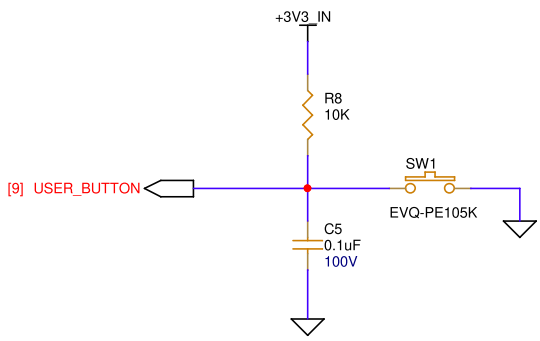
User button
The Dual Buck Evaluation Board has one user button connected to the P9.4 GPIO of the
PSOC™
C3M5 MCU. This general-purpose button is configured for user interaction with the control loop topologies and onboard transient load.
Figure 24. User button
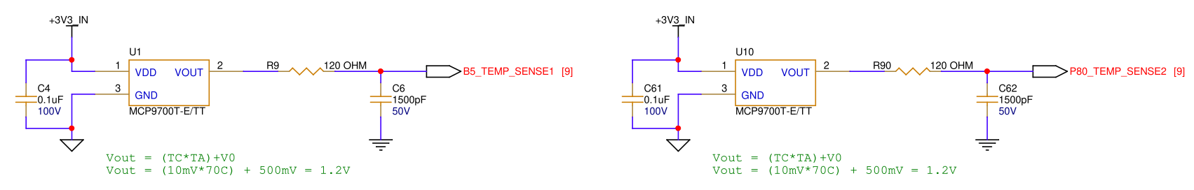
Temperature sensors
The Dual Buck Evaluation Board has two onboard analog temperature sensors in the SOT-23 package (MPN: MCP9700T-E/TT). These sensors have a temperature range of -40°C to +125°C. The output voltage at 0°C is also scaled to 500 mV (typical). The change in voltage is scaled to a temperature coefficient of 10.0 mV/°C (typical). The voltage output pin of these sensors is directly connected to
PSOC™
C3M5 MCU ADC pin B5 and pin P8.0. Temperature sensor U1 is placed close to Buck1 load circuit resistors, and temperature sensor U10 is placed close to Buck2 load circuit resistors.
Figure 25. Temperature sensors
Test points
The following table lists a total of 39 test points within the Dual Buck Evaluation Board. This will help the user to inspect different points of interest and learn how the buck converter performs in detail.
The Dual Buck Evaluation Board also includes a user button (SW1) connected to P9.4 through a 120-pin connector. This can be used by the user to signal the C3M5 MCU when to apply a specific action, for example, enable transient load, change the control scheme, and so on.
Test point number | Test point description |
|---|---|
TP1 | VIN input voltage |
TP2 | VIN resistor divider voltage |
TP3 | Buck1 input current |
TP4 | Buck1 gate driver high-side MOSFET PWM signal |
TP5 | Buck1 HRPWM line signal |
TP6 | Buck1 switching node signal |
TP7 | Buck1 HRPWM complimentary signal |
TP8 | Buck1 gate driver low-side MOSFET PWM signal |
TP9/TP10 | Buck1 injection points for network analyzers |
TP11 | Buck1 VOUT resistor divider voltage |
TP12 | Buck2 input current |
TP13 | Buck2 gate driver high-side MOSFET PWM signal |
TP14 | Buck2 HRPWM line signal |
TP15 | Buck2 switching node signal |
TP16 | Buck2 HRPWM complimentary signal |
TP17 | Buck2 gate driver low-side MOSFET PWM signal |
TP18/TP19 | Buck2 injection points for network analyzers |
TP20 | Buck2 VOUT resistor divider voltage |
TP21 | Buck1 load circuit PWM signal |
TP22 | Buck1 load circuit opamp output signal |
TP23 | Buck1 VOUT voltage |
TP24, TP28, TP31, TP33, TP34, TP37 and TP38 | GND |
TP25 | Buck2 load circuit PWM signal |
TP26 | Buck2 load circuit opamp output signal |
TP27 | Buck2 VOUT voltage |
TP29 | 5 V buck regulator output voltage |
TP30 | 10 V boost regulator output voltage |
TP35 | Buck1 output current |
TP36 | Buck2 output current |
TP32 | AGND |
TP39 | 3.3 V input voltage |
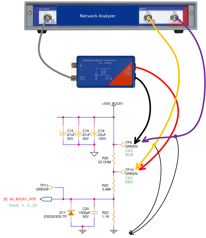
Connection to network analyzer
It is possible to analyze the frequency response of the control loop by injecting on a small shunt resistor a frequency variable signal generated by an external network analyzer. Such a tool is responsible for determining the bandwidth and phase margin of the dual buck converter. In fact, the Dual Buck Evaluation Board includes test points (TP9/TP10 for Buck1 and TP18/TP19 for Buck2) as well as a shunt resistor (R20 for Buck1 and R33 for Buck2) with a resistance value of 22 Ω to help measure the bode diagram of the power stage. The following figure shows how to set up the connection of the Dual Buck Evaluation Board to a network analyzer. The red and black signals represent the injected voltage with variable frequency, whereas the yellow and purple lines represent the measurement paths for the analyzers to capture the amplitude of the transfer function.
Figure 26. Network analyzer connection diagram
120-pin control card connector
The Dual Buck Evaluation Board includes a 120-pin connector compatible with the
PSOC™ Control C3M5
Digital Power Control Card. This connector provides to and receives from the Control Card relevant signals for the control, supply, or communication of the buck converters. The signals available in the connector are as follows:
8 pairs of HRPWM signals (line and complementary)
16 ADC analog inputs
15 general purpose IO pins
Figure 27. 120-pin connector
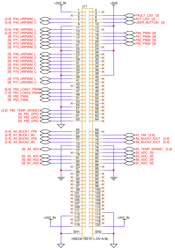
Attention:
The Dual Buck Board 120-pin connector is also providing the power supply for the MCU supply domain.
The pin out of the connector is described in detail in the following table.
Connector pin number | Dual Buck board | Control card | Control card | Dual Buck board | Connector pin number | |
|---|---|---|---|---|---|---|
1 | 3.3 V IN | 3.3 V OUT | XRES | NC | 2 | |
3 | NC | NC | P3.0 | FAULT_LED | 4 | |
5 | P44_HRPWM_L | P4.4 | P3.1 | ACT_LED | 6 | |
7 | P45_HRPWM_C | P4.5 | P9.4 | USER_BUTTON | 8 | |
9 | GND | GND | 5V0 IN | 5V0 OUT | 10 | |
11 | P46_HRPWM_L | P4.6 | NC | NC | 12 | |
13 | P47_HRPWM_C | P4.7 | P9.0 | P90_PWM | 14 | |
15 | P70_HRPWM_L | P7.0 | P9.1 | P91_PWM | 16 | |
17 | P71_HRPWM_C | P7.1 | P9.2 | P92_PWM | 18 | |
19 | P72_HRPWM_L | P7.2 | P9.3 | P93_PWM | 20 | |
21 | P73_HRPWM_C | P7.3 | P9.5 | NC | 22 | |
23 | GND | GND | 5V0 IN | 5V0 OUT | 24 | |
25 | P40_HRPWM_L | P4.0 | NC | NC | 26 | |
27 | P41_HRPWM_C | P4.1 | P0.0/WCO_OUT | NC | 28 | |
29 | P42_HRPWM_L | P4.2 | P0.1/WCO_IN | NC | 30 | |
31 | P43_HRPWM_C | P4.3 | P1.0/ECO_IN | NC | 32 | |
33 | P74_HRPWM_L | P7.4 | P1.1/ECO_OUT | NC | 34 | |
35 | P75_HRPWM_C | P7.5 | NC | NC | 36 | |
37 | GND | GND | 5V0 IN | 5V0 OUT | 38 | |
39 | P76_HRPWM_L | P7.6 | NC | NC | 40 | |
41 | P77_HRPWM_C | P7.7 | P2.2 | NC | 42 | |
51 | NC | NC | P2.3 | NC | 44 | |
45 | P60_LOAD1_PWM | P6.0 | P5.0/SDA | NC | 46 | |
47 | P61_LOAD2_PWM | P6.1 | P5.1/SCL | NC | 48 | |
49 | P62_PWM | P6.2 | P3.2 | NC | 50 | |
51 | P63_PWM | P6.3 | P3.3 | NC | 52 | |
53 | NC | NC | P5.2/UART_RX | NC | 54 | |
55 | GND | GND | P5.3/UART_TX | NC | 56 | |
57 | P80_TEMP_SENSE2 | P8.0 | P8.4 | NC | 58 | |
59 | P81_GPIO | P8.1 | P8.5 | NC | 60 | |
61 | P82_GPIO | P8.2 | NC | NC | 62 | |
63 | P83_GPIO | P8.3 | NC | NC | 64 | |
65 | A0_BUCK1_VFB | AN_A0 | VDDA | NC | 66 | |
67 | A1_BUCK1_IIN | AN_A1 | AN_A7 | A7_VIN | 68 | |
69 | A5_BUCK2_VFB | AN_A5 | AN_A6 | A6_BUCK1_IOUT | 70 | |
71 | A3_BUCK2_IIN | AN_A3 | AN_B4 | B4_BUCK2_IOUT | 72 | |
73 | AGND | AGND | AGND | AGND | 74 | |
75 | A4_ADC | AN_A4 | AN_B5 | B5_TEMP_SENSE1 | 76 | |
77 | NC | VAREF_EXT | AN_B2 | B2_ADC | 78 | |
79 | A2_ADC | AN_A2 | AN_B3 | B3_ADC | 80 | |
81 | B0_ADC | AN_B0 | AN_B6 | B6_ADC | 82 | |
83 | B1_ADC | AN_B1 | AN_B7 | B7_ADC | 84 | |
85 | NC | NC | NC | NC | 86 | |
87 | AGND | AGND | AGND | AGND | 88 | |
89 | NC | NC | NC | NC | 90 | |
91 | NC | NC | NC | NC | 92 | |
93 | NC | NC | NC | NC | 94 | |
95 | NC | NC | NC | NC | 96 | |
97 | NC | NC | NC | NC | 98 | |
99 | NC | NC | NC | NC | 100 | |
101 | NC | NC | NC | NC | 102 | |
103 | NC | NC | NC | NC | 104 | |
105 | NC | NC | NC | NC | 106 | |
107 | NC | NC | NC | NC | 108 | |
109 | NC | NC | NC | NC | 110 | |
111 | NC | NC | GND | GND | 112 | |
113 | GND | GND | P2.0/TDI | NC | 114 | |
115 | NC | P1.2/TCK | P2.1/TDO | NC | 116 | |
117 | NC | P1.3/TMS | VBACKUP | NC | 118 | |
119 | 3.3 V IN | 3.3 V OUT | 3.3 V OUT | 3.3 V IN | 120 |
Protection and fault conditions
The following tables show different fault conditions and protection features on the Dual Buck Evaluation Board.
Parameter | ADC pin voltage | PSOC™ C3M5 pin | Cut off all MOSFETs PWM when any one of the below conditions is true |
|---|---|---|---|
Input voltage | 1.5 V at 24 V VIN | A7 | If VIN is less than 12 V or more than 42 V |
Temperature sensors | 1.3 V at 75 degrees | B5 | If temperature is more than 75 degrees |
1.3 V at 75 degrees | P8.0 | If temperature is more than 75 degrees | |
Output current | 1.5 V at 3 A IOUT1 | A6 | If IOUT1 is more than 3 A |
1.5 V at 3 A IOUT2 | B4 | If IOUT2 is more than 3 A | |
Output voltage | 1.2 V at 5 V VOUT1 | A0 | If VOUT1 is less than 4 V and more than 6 V |
1.2 V at 5 V VOUT2 | A5 | If VOUT2 is less than 4 V and more than 6 V |
Signal | PSOC™ C3M5 pin | Implementation |
|---|---|---|
P60_LOAD1_PWM | P6.0 | 1 Hz PWM signal, 30% Duty cycle |
P61_LOAD2_PWM | P6.1 | 1 Hz PWM signal, 30% Duty cycle |
FAULT_LED | P3.0 | Glows solid when any of the fault conditions are triggered |
ACT_LED | P3.1 | Glows solid when the buck converter is started Blinks when transient load is enabled OFF when the buck converter is stopped |
USER_BUTTON | P9.4 | At 1st press buck converter starts At 2nd press transient load is enabled At 3rd press buck converter is stopped |
Production data
The board has been designed with Allegro. The full PCB design data (schematics, layout, and BOM) of this board can also be downloaded from the
kit webpage
.
Revision history
Document revision | Date | Description of changes |
|---|---|---|
** | 2024-06-18 | Initial release |
*A | 2024-08-01 | Updated the document name Replaced the word "Expansion" with "Evaluation" in the document |
*B | 2024-12-12 | Updated the sections, tables, and figures. |