KIT_PSC3M5_CC1 PSOC™ Control C3M5 Digital Power Control Card user guide
About this document
Scope and purpose
This document describes the features and hardware details of the
PSOC™
Control C3M5 Digital Power Control Card. It is designed to provide an evaluation platform for digital control applications with the
PSOC™
Arm® Cortex®-M33 based MCU. This board is part of Infineon’s digital power evaluation platform kits.
Intended audience
This document is intended for KIT_PSC3M5_CC1 users, and this board is intended to be used under laboratory conditions.
Important notice
“Evaluation Boards and Reference Boards” shall mean
products embedded on a printed circuit board (PCB) for demonstration and/or
evaluation purposes, which include, without limitation, demonstration, reference
and evaluation boards, kits and design (collectively referred to as “Reference
Board”).
Environmental conditions have been considered in
the design of the Evaluation Boards and Reference Boards provided by Infineon
Technologies. The design of the Evaluation Boards and Reference Boards has been
tested by Infineon Technologies only as described in this document. The design
is not qualified in terms of safety requirements, manufacturing and operation
over the entire operating temperature range or lifetime.
The Evaluation Boards and Reference Boards provided
by Infineon Technologies are subject to functional testing only under typical
load conditions. Evaluation Boards and Reference Boards are not subject to the
same procedures as regular products regarding returned material analysis (RMA),
process change notification (PCN) and product discontinuation (PD).
Evaluation Boards and Reference Boards are not
commercialized products, and are solely intended for evaluation and testing
purposes. In particular, they shall not be used for reliability testing or
production. The Evaluation Boards and Reference Boards may therefore not comply
with CE or similar standards (including but not limited to the EMC Directive
2004/EC/108 and the EMC Act) and may not fulfill other requirements of the
country in which they are operated by the customer. The customer shall ensure
that all Evaluation Boards and Reference Boards will be handled in a way which
is compliant with the relevant requirements and standards of the country in
which they are operated.
The Evaluation Boards and Reference Boards as well
as the information provided in this document are addressed only to qualified and
skilled technical staff, for laboratory usage, and shall be used and managed
according to the terms and conditions set forth in this document and in other
related documentation supplied with the respective Evaluation Board or Reference
Board.
It is the responsibility of the customer’s
technical departments to evaluate the suitability of the Evaluation Boards and
Reference Boards for the intended application, and to evaluate the completeness
and correctness of the information provided in this document with respect to
such application.
The customer is obliged to ensure that the use of
the Evaluation Boards and Reference Boards does not cause any harm to persons or
third party property.
The Evaluation Boards and Reference Boards and any
information in this document is provided "as is" and Infineon Technologies
disclaims any warranties, express or implied, including but not limited to
warranties of non-infringement of third party rights and implied warranties of
fitness for any purpose, or for merchantability.
Infineon Technologies shall not be responsible for
any damages resulting from the use of the Evaluation Boards and Reference Boards
and/or from any information provided in this document. The customer is obliged
to defend, indemnify and hold Infineon Technologies harmless from and against
any claims or damages arising out of or resulting from any use thereof.
Infineon Technologies reserves the right to modify
this document and/or any information provided herein at any time without further
notice.
Safety precautions
Note:
Please note the following warnings regarding the hazards associated with development systems.
 | Caution: The evaluation or reference board contains parts and
assemblies sensitive to electrostatic discharge (ESD).
Electrostatic control precautions are required when
installing, testing, servicing or repairing the assembly.
Component damage may result if ESD control procedures are
not followed. If you are not familiar with electrostatic
control procedures, refer to the applicable ESD protection
handbooks and guidelines. |
| Caution: The evaluation or reference board is shipped with packing
materials that need to be removed prior to installation.
Failure to remove all packing materials that are unnecessary
for system installation may result in overheating or
abnormal operating conditions. |
Introduction
Kit contents
The following are the kit contents:
PSOC™
Control C3M5 Digital Power Control Card
PSOC™
Control C3M5 interface Board
USB Type-A to Type-C cable
Quick start guide (printed on the kit package)
Getting started
The following sections will help you get familiar with this evaluation kit:
The Kit operation section describes the major features of the PSOC™ Control C3M5 Digital Power Control Card and functionalities such as programming, debugging, USB-UART, and I2C
The Hardware section provides a detailed hardware description
Application development using the PSOC™ Control C3M5 Digital Power Control Card is supported in ModusToolbox™ software. ModusToolbox™ software is a free development ecosystem that includes the Eclipse IDE for ModusToolbox™ software and the PSOC™ Control C3M5 SDK with the PSOC™ Control C3M5 MCU. Using ModusToolbox™ software, you can enable and configure device resources, middleware libraries, write
C/assemblysource code, program, and debug the device. You can download the software from the ModusToolbox™ home page. See the ModusToolbox™ software installation guide for additional informationThere are a wide range of code examples to evaluate the PSOC™ Control C3M5 Digital Power Control Card. These examples help you familiarize with the PSOC™ Control C3M5 MCU and create your own design. These examples can be accessed through the ModusToolbox™ Project Creator tool. Alternatively,you can also visit Infineon’s code examples for the ModusToolbox™ software page to access these examples
Key features
The
PSOC™
Control C3M5 Digital Power Control Card is equipped with the following features:
Infineon PSOC™ Control C3M5 (Arm® Cortex®-M33 based) MCU PSC3M5FDS2AFQ1, 180 MHz, up to 256 KB flash/64 KB SRAM, E-LQFP-80
Connection to evaluation boards like the Dual Buck Evaluation Board via the 120-pin Edge connector, including analog signals and PWM
Three LEDs
STATUS LED – User-controlled LED
DEBUG LED and COM LED – Debugger controlled LEDs
Isolated debug options (default)
On-Board Debugger (SEGGER J-Link LITE) via USB connector
Isolation needs to be built between this connector and the computer side to avoid overvoltage in the computer
Isolated connectivity
UART channel of the On-Board Debugger (SEGGER J-Link LITE) via USB connector
Two non-isolated debug options (default no load)
SWD/JTAG via a 10-pin 1.27 mm header
SWD/UART via an 8-pin 2.54 mm header
Power supply of PSOC™ Control C3M5
Via evaluation board (5 V) converted to 3.3 V
Via debug USB connector, 5 V DC-DC isolater, and converted to 3.3 V
Power supply of XMC4200 MCU isolated debug domain
Via debug USB connector
Kit operation
The
PSOC™
Control C3M5 Digital Power Control Card is an evaluation board designed to help engineers in learning and testing the digital power control applications. The board features a
PSOC™
Control C3M5 MCU based on an Arm® Cortex®-M33 core. The dimensions of the board (52 mm in height and 57 mm in width to the connector) allow the use of this evaluation card in designs with high requirements on power density. The control card integrates an isolated onboard debugger for a plug-and-play experience. The isolated debugger part can be detached once the code is finalized. In particular, the dimensions of the
PSOC™
Control C3M5 Digital Power Control Card after the isolated debugger is detached (30 mm in height and 57 mm in width to the connector) are suitable for 1U rack designs.
The following figures provide a detailed description of the hardware and its usage.
Figure 1. PSOC™ Control C3M5 Digital Power Control Card hardware description (1)
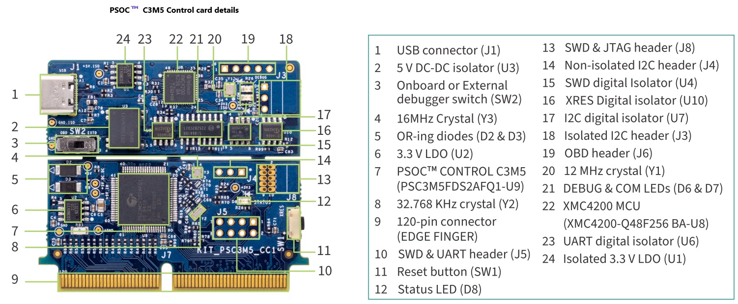
Figure 2. PSOC™ Control C3M5 Digital Power Control Card hardware description (2)
Using the Out of the box example
The
PSOC™
Control C3M5 Digital Power Control Card coming with the interface board is by default programmed with the code example, PSOC™ Control MCU: Hello world. For a detailed description of the project, refer to the example’s
README.md
file in the
GitHub
repository. The
README.md
file is also available in the application directory once the application is created using ModusToolbox™.
Note:
At any point in time, if you overwrite the default application, you can restore it by programming the PSOC™ Control MCU: Hello world.
The following steps describe how to use the code example:
Ensure that the PSOC™ Control C3M5 Digital Power Control Card is mounted on the interface board using the 120-pin Edge connector
Connect the kit to your PC using the provided USB cable through the J-Link USB connector
Open a terminal program and select the COM port. Set the serial port parameters to 8N1 and 115200 baud
Verify that the COM LED on the PSOC™ Control C3M5 Digital Power Control Card is glowing
Press the XRES button (SW1) on the board and confirm that the serial terminal application displays the boot-up message, as shown in Figure 3
Confirm that the user LED (D8) blinks
Follow the instructions on the boot-up message
Figure 3. Serial terminal boot message
Creating a project and program/debug using ModusToolbox™ software
The
PSOC™
Control C3M5 Digital Power Control Card can be programmed and debugged using the onboard JLink debugger. This onboard programmer/debugger supports USB-UART Bridge functionality. An XMC4200 device is used to implement the JLink functionality. For more details on the JLink, see the
J-Link debug probes
.
The following steps briefly introduce project creation, programming, and debugging using ModusToolbox™ software. For detailed instructions, see
.
Connect the board to the PC using the provided USB cable through the JLink USB connector, as shown in Figure 4. It enumerates as a USB composite device if you are connecting it to your PC for the first time
The debugger on this kit is with JLink and one UART. The COM LED (green) is always ON if the USB is connected
Note:
The programming can be done either with the onboard JLink debugger or by attaching an external debugger to the connector J8 on the board. The user can easily switch between the onboard debugger or external debugger by setting the switch SW2 to the desired position. It is recommended to use the onboard JLink debugger.
Figure 4. Connect USB cable to USB connector on the board
In the Eclipse IDE for ModusToolbox™ software, import the desired code example (application) into a new workspace:
In the Quick Panel, click New Application from the Start section
Figure 5. Create new application
Select the BSP-KIT_PSC3M5_CC1 in the Choose Board Support Package window and click Next
Figure 6. Creating a new application: Choose Board Support Package
Select the application in the Select Applicationwindow and click Create
Figure 7.
Creating a new application: Select Application
To build and program a PSOC™ Control C3M5 MCU application:
In the Project Explorer ,select <App_Name> project
In the Quick Panel, click the <App_Name> Program (JLink) configuration from the Launches section, as shown in Figure 8
Figure 8. Programming in ModusToolbox™ software
ModusToolbox™ software has an integrated debugger
To debug a PSOC™ Control C3M5 MCU application:
In the Project Explorer, select <App_Name> project
In the Quick Panel, click the <App_Name> Debug (JLink) configuration from the Launches section, as shown in Figure 9
Figure 9. Debugging in ModusToolbox™ software
For more details, see the Program and debug section in the Eclipse IDE for ModusToolbox™ user guide
Hardware
Hardware functional description
This section explains the individual hardware blocks.
PSOC™ Control C3M5 Digital Power Control Card
Figure 10. Block diagram PSOC™ Control C3M5 Digital Power Control Card
The control card is designed for the PSOC™ C3M5 MCU in an 80-pin LQFP package. There is an onboard isolated JLink debugger implemented with the XMC4200 MCU. All the IOs from the
PSOC™
C3M5 MCU are routed out on a 120-pin Edge finger that can be inserted into a mating connector (MPN: HSEC8-160-01-L-DV-A-BL) on evaluation boards.
PSOC™ Control C3M5 MCU
Figure 11.Block diagram PSOC™ Control C3M5 MCU
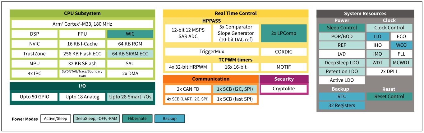
The
PSC3M5xD
devices are based on the Arm® Cortex®-M33, running up to 180 MHz with DSP and FPU capability. In addition to the CPU subsystem, the devices contain advanced real-time control peripherals, such as a high-performance programmable analog subsystem, comparators, advanced timers with high-resolution capability, up to six SCBs, and two CAN FDs for communication. The devices support one active and five low-power modes for managing and reducing power consumption, depending on application requirements.
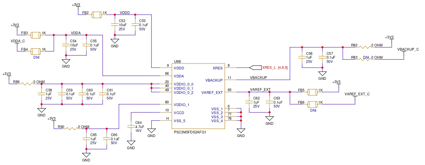
PSOC™ Control C3M5 MCU power supply system
The
PSOC™
C3M5 MCU operates using a single regulated VDDD supply within the range of 1.7 V to 3.6 V. In addition, there is an optional VBACKUP supply that can be used, which has a range of 1.4 V to 3.6 V. A linear regulator powers the core logic at four voltage levels: 0.9 V, 1.0 V, 1.1 V, and 1.2 V. Voltage level switching is implemented by writing to the power control registers. The voltage for the core logic can be set based on the application's performance and power requirements.
Typically, the backup domain requires an input voltage of 1.4 V to 3.6 V, which can be provided by connecting a backup battery or a super capacitor to the VBACKUP pin. The internal backup switch automatically selects between VDDD and VBACKUP (when VDDD is no longer available) for powering the backup domain peripherals like RTC, WCO, ILO, and backup registers. Some I/O cells are powered from the VBACKUP supply before the internal backup switch. If the application does not require a dedicated backup source, VBACKUP can be connected to VDDD externally to ensure that the I/O cells powered by VBACKUP are functional.
Figure 12. PSOC™ Control C3M5 Digital Power Control Card power tree (1)
Figure 13. PSOC™ Control C3M5 Digital Power Control Card power tree (2)
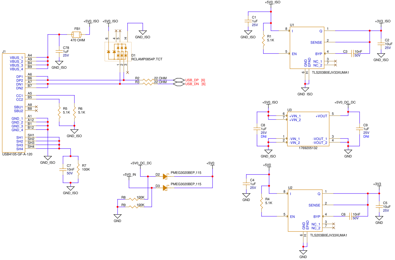
Figure 14. PSOC™ C3M5 power supply system
The control card is fully functional either when connected as a standalone through a USB Type-C connector to an external source, such as a laptop, or by receiving 5 V power from the evaluation board since 5 V power is provided on the 120-pin Edge connector.
PSOC™
C3M5 is in fact supplied from an isolated 3.3 V LDO, which is powered through an isolated DC-DC 5 V OR’ ed with an evaluation board at 5 V. The XMC4200 JLink is powered by a 3.3 V LDO, which is powered by a USB Type-C connector at 5 V. Also, the 3.3 V generated on the control card is routed to a 120-pin Edge connector for the evaluation board.
PSOC™
Control C3M5 MCU I/Os
Figure 15.
PSOC™
C3M5 MCU IOs
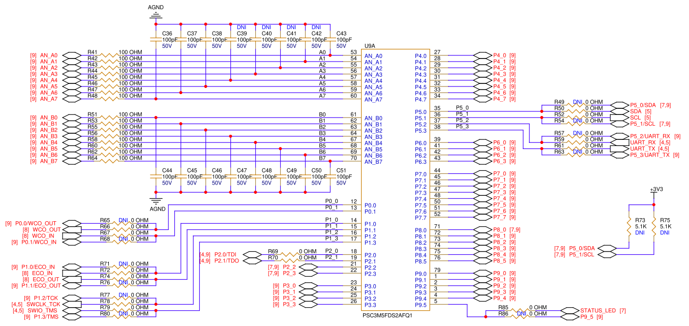
The
PSOC™
C3M5 Control Card will bring out all the IOs to the 120-pin Edge finger. The ECO, WCO, SWD/JTAG, UART, and I2C pins are dedicated to the board by default and routed to the Edge finger with zero-ohm options.
120-pin Edge finger interface
Figure 16.
120-pin Edge finger
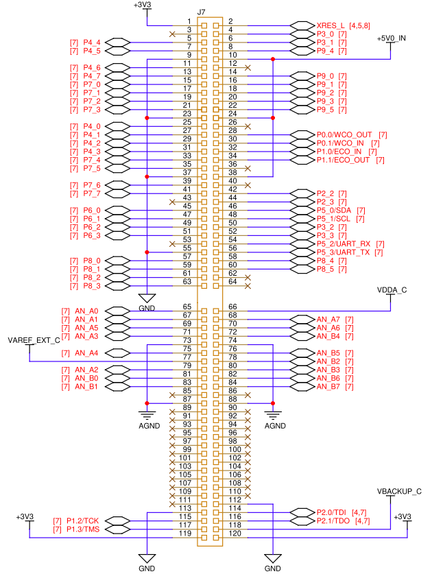
The control card has a 120-pin Edge finger, which is inserted into a mating connector (HSEC8-160-01-L-DV-A-BL) on evaluation boards. All the IO lines of the
PSOC™
C3M5 device are routed to this 120-pin Edge finger. The control card pinout is defined so that it can be used as a generic control card for various types of evaluation boards. There will be different kinds of evaluation boards, such as Dual Buck Evaluation Board, PFC Evaluation Board, and so on. All these evaluation boards are built such that the 120-pin connector on them is compatible with this control card pinout. The edge connector has a 5 V input supply to the control card and a 3.3 V output supply from the control card.
The following are the signals available on the edge finger:
Eight pairs of HRPWM signals (line and complimentary)
16 ADC analog inputs
One UART channel
One I2C channel
JTAG signals
22 general purpose IO pins
Analog-to-digital converter (ADC) input filter
Figure 17.
ADC input RC filter
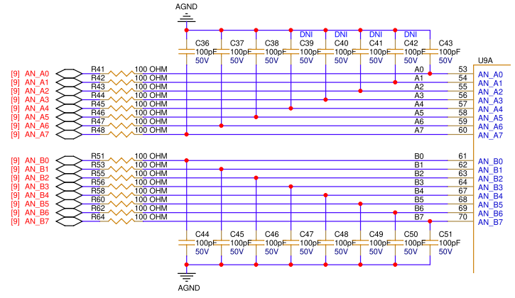
All ADC inputs on the control card are filtered with a high-frequency cross-over frequency RC filter, as shown in
Figure 17
. This will help to remove undesired high-frequency noise from the input signals. As a result, it will improve the measurement performance of the MCU.
Reset button
Figure 18.
Reset button
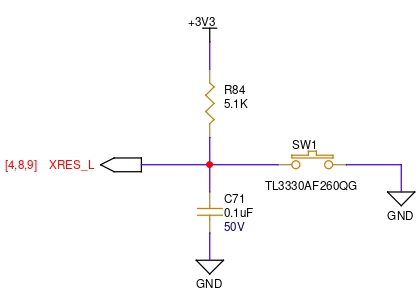
The control card contains one reset button (SW1) for resetting the
PSOC™
Control C3M5 MCU. When this SW1 button is pressed, the XRES_L line of the
PSOC™
Control C3M5 MCU is pulled to the ground, which in turn resets the target device.
LEDs
Figure 19.
LEDs
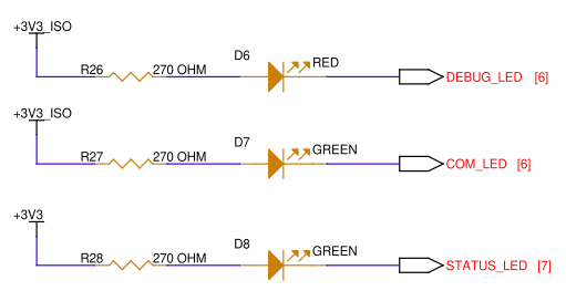
The control card contains three discrete LEDs:
One user-controlled LED D8 (green-STATUS LED) is connected to the P9.5 GPIO of the
PSOC™
C3M5 MCU. This user LED is active low, so the P9.5 pin must be driven low to turn ON this LED
Two debug controller LEDs, D6 (red-DEBUG LED) and D7 (green-COM LED), are connected to XMC4200 MCU pins and are not user-controlled
Digital isolators
Figure 20.
Digital isolators
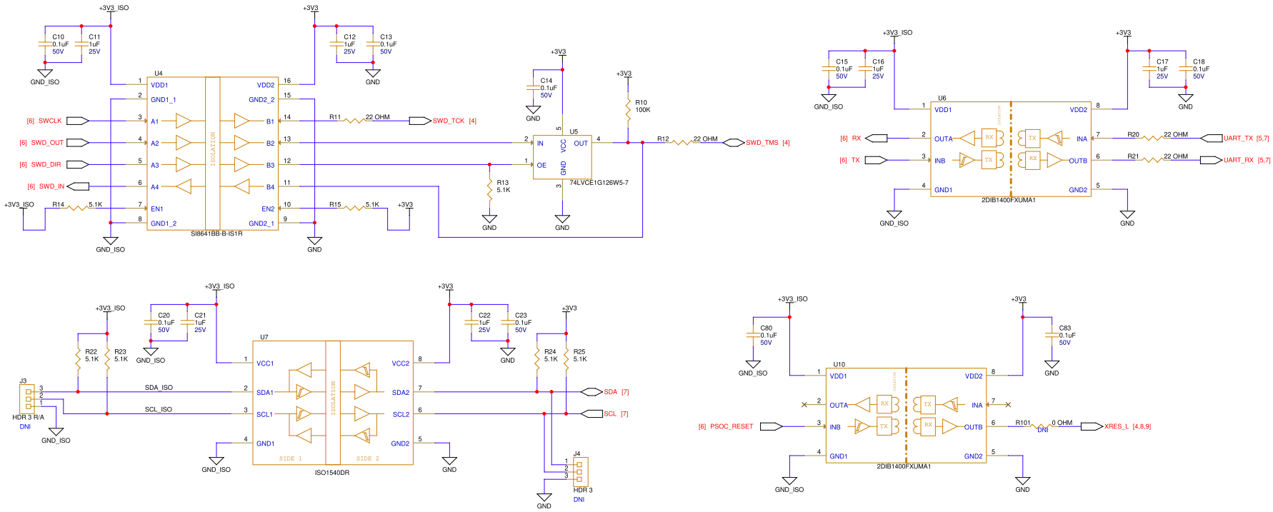
The control card has an onboard XMC4200-based JLink debugger. All the signals connected between the XMC4200 and
PSOC™
C3M5 devices are isolated with digital isolators. These digital isolators can provide capacitive isolation up to 2.5 KVrms. Also, there is a DC-DC isolator that provides 5 V to 5 V isolation between the XMC4200 and
PSOC™
C3M5 sides. All the digital isolators are placed on the breakable side of the control card. When the user breaks off the debugger section of the PCB, the control card will not have any isolation. There are a total of four digital isolators on the control card, with 9 (4+2+2+1) channels. A 4-channel digital isolator is used for SWD interface isolation; a 2-channel digital isolator is connected between UART lines; one isolation channel is used to connect the
PSOC™
C3M5 XRES pin to the XMC4200 P0.3 pin, and another 2-channel bidirectional digital isolator is used for I2C interface isolation. This isolated I2C interface can be accessed through a 3-pin header (J3). This same I2C interface can also be accessed from another 3-pin header (J4) directly from
PSOC™
C3M5 MCU pins, which are not isolated. The user must make sure while accessing I2C through the J4 header to use external galvanic isolation (typically 1 kV) to avoid damage due to high voltages in the computer.
PSOC™
C3M5 Interface Board
Figure 21.
PSOC™
C3M5 Interface Board schematics
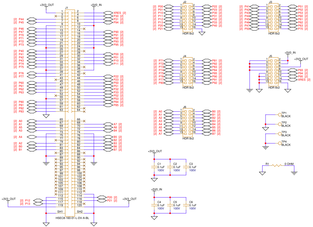
Figure 22.
PSOC™
C3M5 Interface board
Figure 23.
PSOC™
C3M5 Interface Board and Control Card
The interface board is made as an interface for the
PSOC™
C3M5 Control Card. When no evaluation board is present, this interface board can be used to easily access the IO pins of the
PSOC™
C3M5 controller. The interface board has a 120-pin mating connector (HSEC8-160-01-L-DV-A-BL) and five numbers of 2.54 mm 2x8 headers. The interface board does not require any power as it has no active components. When the
PSOC™
C3M5 Control Card is not powered through the USB Type-C connector, a 5 V input can be supplied to it through the J5 header of the interface board. The control card provides a 3.3 V rail to the interface board, with the current limited to less than 100 mA.
PSOC™
Control C3M5 MCU clock architecture
Figure 24.
PSOC™
C3M5 clock sources
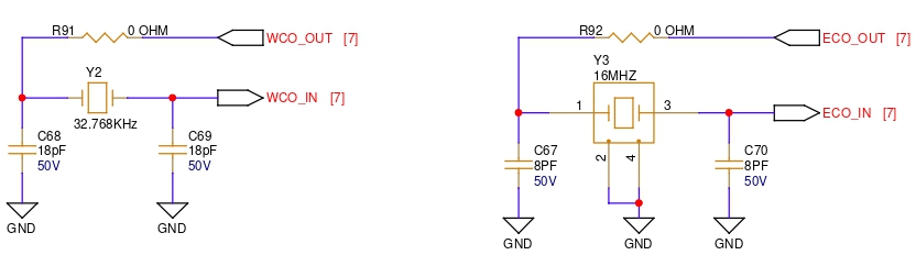
The control card includes 16 MHz ECO (Y3) and 32.768 kHz WCO (Y2) for the
PSOC™
Control C3M5 MCU device.
PSOC™
Control C3M5 MCU external program/debug headers
Figure 25.
PSOC™
C3M5 external program/debug headers
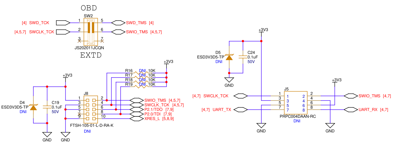
The control card has an isolated XMC4200 MCU-based JLink programmer/debugger onboard. Alternately, the
PSOC™
Control C3M5 MCU can be programmed through a 10-pin SWD/JTAG header (J8) using MiniProg4 or any third-party programmer. Switch SW2 let users select between onboard debugger (OBD) or external debugger (EXTD). The user must make sure that the external debugger box used provides galvanic isolation (typically 1 kV) to avoid damage due to high voltages in the computer.
PSOC™
Control C3M5 MCU or any other onboard peripheral cannot be powered from the 10-pin SWD/JTAG header (J8). This is to protect the external programmer from overloading, making sure that the kit does not draw any current from the external programmer through J8. Additionally, an 8-pin SWD/UART header (J5) is also provided for programming or debugging the
PSOC™
Control C3M5 MCU.
PSOC™
Control C3M5 Digital Power Control Card includes two external connector options (J8 and J5) for debugging. The default configuration of the control card is prepared for onboard JLINK debug with switch SW2 set to the OBD position, and therefore, none of the two connector options (J8 and J5) are assembled. If required, the user has to mount the corresponding headers (J8 or J5) and make sure to set the switch SW2 to the EXTD position on the control card.
XMC4200 as onboard programmer/debugger
Figure 26.
XMC4200 MCU based on board JLink programmer/debugger
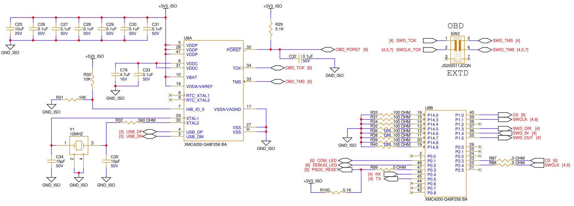
The
PSOC™
Control C3M5 Digital Power Control Card supports on board isolated debug interface:
XMC4200-based JLink-isolated On-Board Debugger (OBD). Switch SW2 is set to the OBD position to support the onboard debugger. This is the default connection. It is powered through a USB Type-C connector (5 V) converted to an isolated 3.3 V
The control card includes a debugger controller and isolation up to 2.5 kV to protect the computer. Connect the Control card to a computer with a USB cable.
The on board debugger (OBD) supports:
Serial Wire Debug (SWD)
UART communication via a virtual COM port
Note:
The firmware of the OBD requires the latest JLink driver and a serial port driver (CDC driver) installed on your computer. Check “Install J-Link Serial Port Driver” when installing the latest JLink driver.
Removing the onboard debugger
Figure 27.
Debug options when removing debugger part of control card
PSOC™
Control C3M5 Digital Power Control Card can be broken off into two parts by breaking the PCB, as shown in
Figure 27
. This will reduce the size of the main controller part so that it can fit into 1U standard-sized rack systems once programmed. The control card can still be debugged in two different ways if the debugger part is removed.
Connecting a ribbon cable to an 8-pin connector (J5) or,
Using the 10-pin connector (J8) option with an external debugger box
By default, these connectors (J8 and J5) are not loaded. The user can install these connectors when the onboard debugger is broken. When the onboard debugger is not broken and these J5 or J8 connectors are installed, then the user must make sure to set the switch SW2 to the EXTD position to make the external debugger work.
Note:
When using external debuggers, make sure that the debugger box includes galvanic isolation for the computer. If the control card is exposed to high voltages, this can cause damage to the computer.
Production data
The board has been designed with Allegro. The full PCB design data (schematics, layout, and BOM) of this board can also be downloaded from the
kit webpage
.
Revision history
Document revision | Date | Description of changes |
|---|---|---|
** | 2024-07-16 | Initial release |
*A | 2024-08-01 | Replaced the word "Expansion" with "Evaluation" in the document |
*B | 2024-12-16 | Updated: Using the Out of the box example Creating a project and program/debug using ModusToolbox™ software PSOC™ Control C3M5 Digital Power Control Card PSOC™ Control C3M5 MCU external program/debug headers XMC4200 as onboard programmer/debugger Publish to web |