KIT_PSC3M5_CC2 PSOC
Control C3 Motor Control Evaluation Kit guide
About this document
Scope and purpose
This document describes the features and hardware details of the PSOC™ Control C3M5 motor control card, which is designed to serve as an evaluation platform for motor control applications with the PSOC™ Arm® Cortex®-M33 based microcontroller. This board is part of Infineon’s motor control evaluation platform kits.
Intended audience
This document is intended for
KIT_PSC3M5_CC2
users. This board is intended to be used under laboratory conditions.
Reference board/kit
Product(s) embedded on a PCB with a focus on specific applications and defined use cases that may include software. PCB and auxiliary circuits are optimized for the requirements of the target application.
Note:
Boards do not necessarily meet safety, EMI, quality standards (for example UL, CE) requirements.
Important notice
“Evaluation Boards and Reference Boards” shall mean
products embedded on a printed circuit board (PCB) for demonstration and/or
evaluation purposes, which include, without limitation, demonstration, reference
and evaluation boards, kits and design (collectively referred to as “Reference
Board”).
Environmental conditions have been considered in
the design of the Evaluation Boards and Reference Boards provided by Infineon
Technologies. The design of the Evaluation Boards and Reference Boards has been
tested by Infineon Technologies only as described in this document. The design
is not qualified in terms of safety requirements, manufacturing and operation
over the entire operating temperature range or lifetime.
The Evaluation Boards and Reference Boards provided
by Infineon Technologies are subject to functional testing only under typical
load conditions. Evaluation Boards and Reference Boards are not subject to the
same procedures as regular products regarding returned material analysis (RMA),
process change notification (PCN) and product discontinuation (PD).
Evaluation Boards and Reference Boards are not
commercialized products, and are solely intended for evaluation and testing
purposes. In particular, they shall not be used for reliability testing or
production. The Evaluation Boards and Reference Boards may therefore not comply
with CE or similar standards (including but not limited to the EMC Directive
2004/EC/108 and the EMC Act) and may not fulfill other requirements of the
country in which they are operated by the customer. The customer shall ensure
that all Evaluation Boards and Reference Boards will be handled in a way which
is compliant with the relevant requirements and standards of the country in
which they are operated.
The Evaluation Boards and Reference Boards as well
as the information provided in this document are addressed only to qualified and
skilled technical staff, for laboratory usage, and shall be used and managed
according to the terms and conditions set forth in this document and in other
related documentation supplied with the respective Evaluation Board or Reference
Board.
It is the responsibility of the customer’s
technical departments to evaluate the suitability of the Evaluation Boards and
Reference Boards for the intended application, and to evaluate the completeness
and correctness of the information provided in this document with respect to
such application.
The customer is obliged to ensure that the use of
the Evaluation Boards and Reference Boards does not cause any harm to persons or
third party property.
The Evaluation Boards and Reference Boards and any
information in this document is provided "as is" and Infineon Technologies
disclaims any warranties, express or implied, including but not limited to
warranties of non-infringement of third party rights and implied warranties of
fitness for any purpose, or for merchantability.
Infineon Technologies shall not be responsible for
any damages resulting from the use of the Evaluation Boards and Reference Boards
and/or from any information provided in this document. The customer is obliged
to defend, indemnify and hold Infineon Technologies harmless from and against
any claims or damages arising out of or resulting from any use thereof.
Infineon Technologies reserves the right to modify
this document and/or any information provided herein at any time without further
notice.
Safety precautions
 | Caution: The heat sink and device surfaces of the evaluation or
reference board may become hot during testing. Hence,
necessary precautions are required while handling the board.
Failure to comply may cause injury. |
 | Caution: Only personnel familiar with the drive, power electronics and
associated machinery should plan, install, commission and
subsequently service the system. Failure to comply may
result in personal injury and/or equipment damage. |
| Caution: The evaluation or reference board contains parts and
assemblies sensitive to electrostatic discharge (ESD).
Electrostatic control precautions are required when
installing, testing, servicing or repairing the assembly.
Component damage may result if ESD control procedures are
not followed. If you are not familiar with electrostatic
control procedures, refer to the applicable ESD protection
handbooks and guidelines. |
| Caution: A drive that is incorrectly applied or installed can lead to
component damage or reduction in product lifetime. Wiring or
application errors such as undersizing the motor, supplying
an incorrect or inadequate AC supply, or excessive ambient
temperatures may result in system malfunction. |
| Caution: The evaluation or reference board is shipped with packing
materials that need to be removed prior to installation.
Failure to remove all packing materials that are unnecessary
for system installation may result in overheating or
abnormal operating conditions. |
Introduction
Kit contents
The kit comprises the following contents:
KIT_PSC3M5_CC2 motor control card
Drive adapter card
USB Type-A to USB Type-C cable
Quick start guide
Getting started
This guide is designed to familiarize you with the evaluation kit.
The
Kit operation
section describes the major features and functionalities, such as programming, debugging, and USB-UART bridges of the PSOC™ Control C3M5 motor control card
The
Hardware section
provides a detailed hardware description
Application development using the PSOC™ Control C3M5 motor control card is supported in ModusToolbox™. ModusToolbox™ is a free development ecosystem that includes the Eclipse IDE for ModusToolbox™ and the PSOC™ Control C3M5 SDK along with PSOC™ Control C3M5 MCU. Using ModusToolbox™, you can enable and configure device resources, middleware libraries, write C/assembly source codes, and program or debug the device. For more information, see the
ModusToolbox™ software installation guide
Code examples are available for evaluating the PSOC™ Control C3M5 motor control card. These examples help you familiarize yourself with the PSOC™ Control C3M5 MCU and create your own designs. These examples can be accessed through the
ModusToolbox™ Project Creator
tool. Additionally, see
Infineon code examples for ModusToolbox™ software
to access these examples
Key features
The PSOC™ Control C3M5 motor control card is equipped with the following features:
Infineon PSOC™ Control C3M5 (Arm® Cortex®-M33 based) microcontroller
PSC3M5FDS2AFQ1
, 180 MHz, up to 256 KB flash/64 KB SRAM, E-LQFP-80
Connection to MADK boards (M1/M3/M5) via 100-pin HD connector connected to the XMC™ drive adapter card
Five LEDs
:
1 Power LED
2 User LEDs: User-controlled LED
2 Debug LEDs and Aux LEDs: Debugger-controlled LEDs
Isolated debug options (default)
:
Onboard isolated debugger (SEGGER J-Link Lite) via USB connector
Isolated connectivity
:
UART channel of on-board debugger (SEGGER J-Link Lite) via USB connector
CAN interface on a 4-pin header X14
2 non-isolated debug options
:
SWD/JTAG 10-pin 1.27 mm header
ETM 20-pin 1.27 mm header
Power supply
:
PSOC™ Control C3M5 MCU
:
Via 100-pin expansion board (5 V or 24 V) converted to 3.3 V
Via debug USB connector, 5 V isolated DC-DC converted to 3.3 V
XMC4200 MCU in isolated debug domain
:
Via debug USB connector
Kit operation
The PSOC™ Control C3M5 motor control card is an evaluation board designed to assist engineers in developing PSOC™ Control C3-based motor control solutions in combination with suitable power stage evaluation boards featuring the MADK connector (M1/M3/M5). The board features an isolated onboard debugger for programming and debugging over a USB interface. Additionally, it features USB VCOM functionality using the same USB connection as the debugger.
Figure 1.
KIT_PSC3M5_CC2 motor control card block diagram
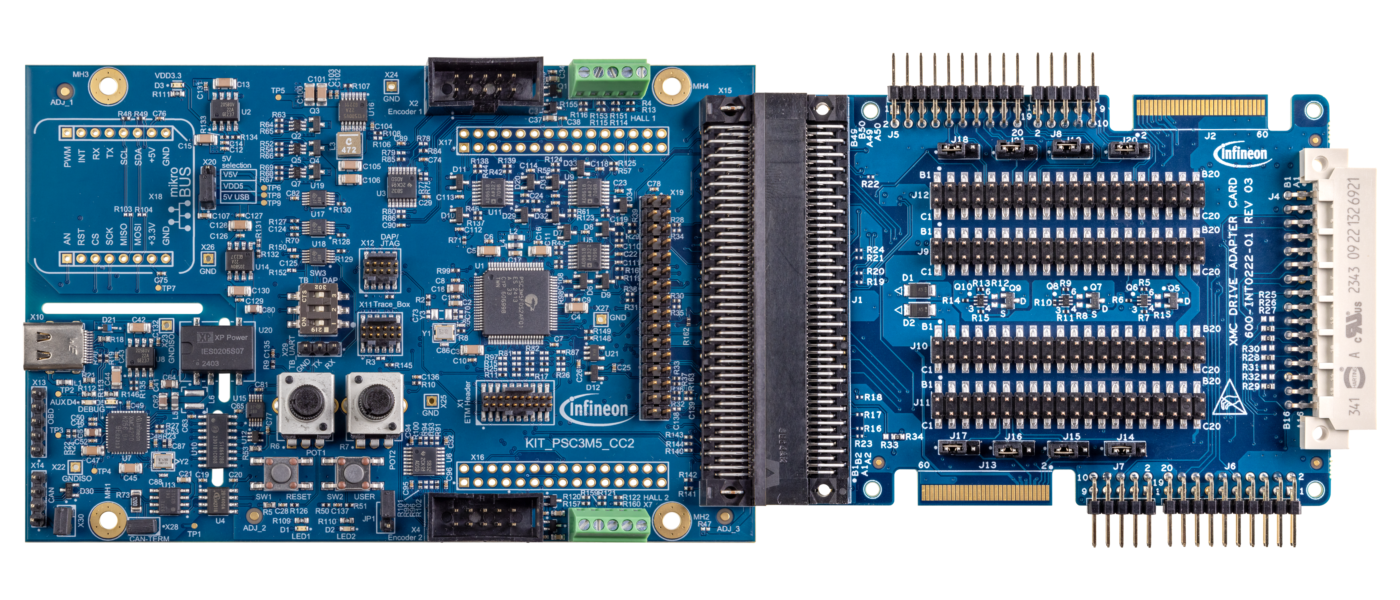
Figure 2.
KIT_PSC3M5_CC2 motor control card details
Isolated DC-DC (U20)
USB Type-C socket (X10)
Debug LED (D5) and Aux LED (D4)
XMC4200 MCU(J-Link - U7)
Isolated CAN header (X14)
SWD/UART and CAN isolators (U10, U4)
User button (SW2) and Reset button (SW1)
User LED1 (D1) and User LED2 (D2)
Potentiometers (R6, R7)
Motor 2 encoder input (X4)
ETM header (X1)
Motor 2 Hall sensor input (X7)
100-pin HD connector (X15)
MADK M5 pinout header (X19)
Motor 1 Hall sensor input (X3)
PSC3M5FDS2AFQ1 Target MCU (U1)
Motor 1 encoder input (X2)
10-pin SWD/JTAG header (X12)
Debug interface selection (SW3)
Supply selection jumper (X20)
mikroBUS header (X18)
Figure 3.
Drive adapter card details
100-pin HD connector (J1)
2x20 headers (J9, J10, J11, J12)
Samtec connector 2 (J13)
MADK M1 connector 2 (J6) and MADK M3 connector 2 (J6 + J7)
MADK M5 connector (J4)
Samtec connector 1 (J2)
MADK M1 connector 1 (J5) and MADK M3 connector 1 (J5 + J8)
Figure 4.
KIT_PSC3M5_CC2 motor control card connected to the drive adapter card
Using the OOB example
The PSOC™ Control C3M5 motor control card is, by default, programmed with the
Hello World
code example. For a detailed description of the project, see the example’s
README.md
file in the GitHub repository. The
README.md
file is also available in the application directory once the application is created.
Note:
At any point in time, if you overwrite the default application, you can restore it by programming the Hello World code example.
To use the code example, do the following:
Connect the kit to the PC using the provided USB cable
Verify that the debug LED on the board is glowing
Open a terminal program such as Tera Term or Minicom and select the J-Link VCOM port. Set the serial port parameters to 8N1 and 115200 baud
Press the
XRES button (SW1)
on the board and confirm that the serial terminal application displays the bootup message as shown in
Figure 5
Confirm that the user
LED1 (D1)
is blinking
Follow the instructions shown in the bootup message
Figure 5.
Serial terminal boot message

Creating a project and programming/debugging using ModusToolbox
The PSOC™ Control C3M5 motor control card can be programmed and debugged using the onboard J-Link debugger. This onboard programmer/debugger supports a USB-UART bridge. An XMC4200 device is used to implement the J-Link functionality. See the
J-Link user guide
for more details.
The following steps briefly introduce project creation, programming, and debugging using ModusToolbox™. For detailed instructions, see
Connect the board to the PC using the provided USB cable through the J-Link USB connector (X10), as shown in
Figure 6
. It enumerates as a USB composite device if you are connecting it to your PC for the first time
Figure 6.
Connect USB cable to the USB connector on board
The debugger on this kit features the J-Link Lite with UART. The debug LED (green) is always ON if the USB is connected
Note:
The programming can be done either with the onboard J-Link debugger (isolated) or by attaching an external debugger to the connector X12 (non-isolated) on the board. It is recommended to use the onboard J-Link debugger
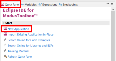
In the Eclipse IDE for ModusToolbox™, import the desired code example (application) into a new workspace
Click on
New Application
from the Quick Panel tab
Figure 7.
Create new application
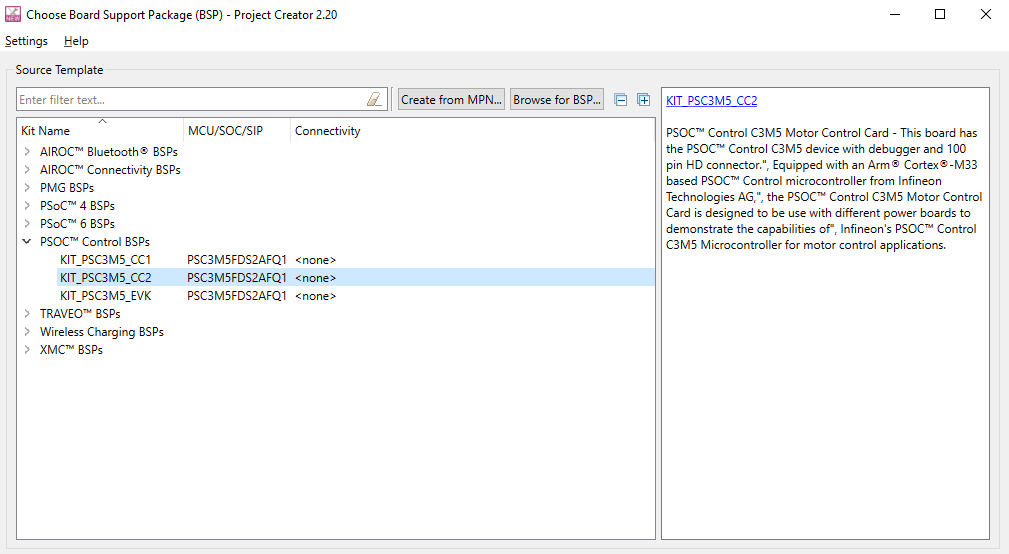
In the Choose Board Support Package (BSP) window, expand the PSOC™ Control BSPs, select the
KIT_PSC3M5_CC2
BSP, and click
Next
Figure 8.
Choose Board Support Package
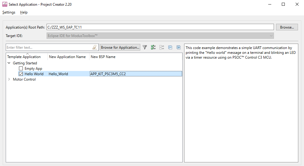
In the Select Application window, expand the Getting Started section, select the
Hello World
application, and click
Create
Figure 9.
Select application
To build and program the PSOC™ Control C3M5 MCU application, do the following:
In the Project Explorer, select the
<App_Name>
project
In the Quick Panel tab, scroll to the
Launches
Click the
<App_Name> Program (J-Link)
configuration
Figure 10.
Programming in ModusToolbox™
ModusToolbox™ software has an integrated debugger. To debug a PSOC™ Control C3M5 MCU application:
In the Project Explorer, select the
<App_Name>
project
In the Quick Panel, scroll to the Launches section and click the
<App_Name> Debug (J-Link)
configuration. For more information, see the Program and debug section in the
Eclipse IDE for ModusToolbox™ user guide
Figure 11.
Debugging in ModusToolbox™
Hardware
Hardware functional description
This section provides a detailed explanation of the individual hardware blocks used in this kit.
PSOC™ Control C3M5 motor control card
The control card is designed for the PSOC™ Control C3M5 microcontroller in an E-LQFP-80 package. The onboard isolated J-Link debugger is implemented using the XMC4200 microcontroller. All the I/Os from the PSOC™ Control C3M5 MCU are routed out to the 100-pin high-density (HD) connector, which can be inserted into a mating connector on the included adapter board. The adapter board, in turn, provides connectivity to the motor control power boards using MADK M1/M3, M5, and Samtec connectors.
PSOC™ Control C3M5 MCU
Figure 12.
PSOC™ Control C3M5 MCU block diagram
The PSC3M5xD devices are based on the Arm® Cortex®-M33 microcontroller, running at up to 180 MHz with DSP and FPU capabilities. In addition to the CPU subsystem, the devices contain advanced real-time control peripherals, such as a high-performance programmable analog subsystem, comparators, advanced timers with high-resolution capability, up to six serial communication blocks (SCBs), and two CAN FDs for communication. The devices support one Active mode and five low-power modes for managing and reducing power consumption depending on application requirements.
Figure 13.
PSOC™ Control C3 MCU pin connections
PSOC™ Control C3M5 MCU power supply system
The PSOC™ C3M5 MCU operates using a single regulated VDDD supply within the range of 1.71 V to 3.6 V. Additionally, there is an optional VBACKUP supply, which has a range of 1.4 V to 3.6 V. A linear regulator powers the core logic at four voltage levels: 0.9 V, 1.0 V, 1.1 V, and 1.2 V. Voltage level switching is implemented by writing to the power control registers. The voltage for the core logic can be set based on the application's performance and power requirements.
Typically, the backup domain requires an input voltage of 1.4 V to 3.6 V, which can be provided by connecting a backup battery or a supercapacitor to the VBACKUP pin. The internal backup switch automatically selects between VDDD and VBACKUP (when VDDD is no longer available) for powering the backup domain peripherals like the RTC, WCO, ILO, and backup registers. Some I/O cells are powered from the VBACKUP supply before the internal backup switch. If the application does not require a dedicated backup source, VBACKUP can be connected to VDDD externally to ensure that the I/O cells powered by VBACKUP are functional.
Figure 14.
PSOC™ Control C3 MCU power supply scheme
The PSOC™ Control C3 MCU operates at 3.3 V, while the rest of the board requires both 3.3 V and 5 V supplies. The VDD3.3, used to power the MCU, is generated using the U2 low-dropout regulator. The VDD5 rail, which powers this regulator as well as the rest of the circuits running on 3 V or 5 V, can be sourced from any of the following options:
Isolated USB supply
: The USB 5 V supply is used to power a 5 V to 7 V DC-DC isolated converter, which in turn generates a 5 V supply, VDCDC5, using U14. This supply can be used to power the board when the X20 jumper is set to the 1-2 position
5 V or 24 V supply from the power board
: When the X20 jumper is set to the 2-3 position, the board can be powered by any of the following sources:
High-density HD connector (X15)
: Either a 24 V supply on pin B41, converted to 5 V using U16, or a 5 V supply on pins B5/B10 of the 100-pin high-density connector
MADK5 power board header (X19)
: A 5 V supply on pin 2 of the X19 header can be used to power the board
Multiple 5 V sources, which come from the power stage (either direct 5 V or 24 V regulated to 5 V), are ORed using low-drop rectifiers based on the Q3, Q4, and Q6 MOSFETs.
PSOC™ Control C3M5 MCU I/O connectors
Figure 15.
MADK M5 header, expansion headers, and mikroBUS header
MADK M5 header (X19)
: The MADK M5 header provides the same pinout available in the MADK M5 connector on the drive adapter card, using a 16x2 male header with a standard 2.54 mm pitch. This header can be used for hardware debugging or probing signals.
Pin no. | Signal name | PSC3M5 pin | Description |
|---|---|---|---|
1 | GND | GND | Ground |
2 | VPWR5V | NA | Power input |
3 | PFC_Gate1 | P6.0 | PFC gate PWM signal |
4 | P8_1_PFC_Relay2 | P8.1 | PFC relay GPIO output |
5 | AN_A5_VBEMF_U/IU(3) 1 | AN_A5 | PFC current sense signal (pin B45 of X15) |
6 | AN_B6_BrakeTemp1 | AN_B6 | Temperature feedback for motor 1 power stage |
7 | AN_B7_IAVG_IDCLink(3) 2 | AN_B7 | PFC bus voltage sensing (pin A46 on X15) |
8 | AN_A4_VDCLink | AN_A4 | Power stage VDC link sense signal |
9 | AN_A0_VBEMF_U/IU(1) | AN_A0 | Motor 1 BEMF U or Current U sense |
10 | AN_B0_VBEMF_U/IU(2) | AN_B0 | Motor 2 BEMF U or Current U sense |
11 | AN_A1_VBEMF_V/IV(1) | AN_A1 | Motor 1 BEMF V or Current V sense |
12 | AN_B1_VBEMF_V/IV(2) | AN_B1 | Motor 2 BEMF V or Current V sense |
13 | AN_A2_VBEMF_W/IW(1) | AN_A2 | Motor 1 BEMF W or Current W sense |
14 | AN_B2_VBEMF_W/IW(2) | AN_B2 | Motor 2 BEMF W or Current W sense |
15 | AN_A3_IAVG/IDCLink(1) | AN_A3 | Motor 1 DC link shunt current |
16 | AN_B3_IAVG/IDCLink(2) | AN_B3 | Motor 2 DC link shunt current |
17 | P8_3_U2_L | P8.3 | Motor 2 PWM UL |
18 | P4_1_U1_L | P4.1 | Motor 1 PWM UL |
19 | P8_2_U2_H | P8.2 | Motor 2 PWM UH |
20 | P4_0_U1_H | P4.0 | Motor 1 PWM UH |
21 | P9_1_V2_L | P9.1 | Motor 2 PWM VL |
22 | P4_3_V1_L | P4.3 | Motor 1 PWM VL |
23 | P9_0_V2_H | P9.0 | Motor 2 PWM VH |
24 | P4_2_V1_H | P4.2 | Motor 1 PWM VH |
25 | P9_3_W2_L | P9.3 | Motor 2 PWM WL |
26 | P4_5_W1_L | P4.5 | Motor 1 PWM WL |
27 | P9_2_W2_H | P9.2 | Motor 2 PWM WH |
28 | P4_4_W1_H | P4.4 | Motor 1 PWM WH |
29 | P7_7_KILL_2 | P7.7 | Motor 2 kill feedback |
30 | P8_0_KILL_1 | P8.0 | Motor 1 kill feedback |
31 | P8_5_ENPOW2 | P8.5 | Motor 2 power stage enables |
32 | P8_4_ENPOW1 | P8.4 | Motor 1 power stage enables |
mikroBUS header (X18)
: The mikroBUS header provides a standardized interface for connecting compatible Click boards, which can expand the kit's functionality with sensors, actuators, communication modules, and more. Note that some interfaces may require rework, as the same pins are used for multiple functionalities.
Note:
Since SPI and I
2
C use the same SCB pins, only one of these interfaces can be used at a time.
Pin | Signal name | Connected to signal | PSC3 MCU pin | Rework required |
|---|---|---|---|---|
1 | AN | Vac0/POT1 | AN_B4 | Y |
2 | RST | XRES_L | XRES | |
3 | CS | SCB3 SPI CS | P5.3 | |
4 | SCK | SCB3 SPI SCK | P5.2 | |
5 | MISO | SCB3 SPI MISO | P5.1 | |
6 | MOSI | SCB3 SPI MOSI | P5.0 | |
7 | +3.3 V | VDD3.3 | VDDD | |
8 | GND | GND | EPAD | |
9 | GND | GND | EPAD | |
10 | +5 V | VDD5 | ||
11 | SDA | SCB3 I2C SDA | P5.0 | Y |
12 | SCL | SCB3 I2C SCL | P5.1 | Y |
13 | TX | SCB1 UART RX | P2.2 | |
14 | RX | SCB1 UART TX | P2.3 | |
15 | INT | GPIO interrupt | P0.0 | |
16 | PWM | TCPWM line out | P0.1 |
Note:
mikroBus header pin 1 AN input is also connected to POT1. Remove R9 to use this pin for an external analog input.
1
The AN_A5_VBEMF_U/IU(3) net is connected to pin B45 of the 100-pin high-density connector and is used for PFC current sensing (ANALOG_PFC_I1 signal).
2
The AN_B7_IAVG_IDCLink(3) net is connected to pin A46 of the 100-pin high-density connector and is used for PFC voltage sensing (ANALOG_PFC_VDCLINK signal).
100-pin HD connector interface
Figure 16.
100-pin HD connector
The 100-pin HD connector interfaces with the drive adapter card, providing connectivity for MADK motor power stages. It supports single and dual motors, as well as optional power factor correction (PFC) control or a third motor.
X15 HD pin | PSC3 pin | Peripherals | X15 HD pin | PSC3 pin | Peripherals |
|---|---|---|---|---|---|
A1 | P7.0 | SCB2 SCL | B1 | P7.1 | SCB2 SDA |
A2 | P7.0 | SCB2 CLK | B2 | P7.1 | SCB2 MOSI |
A3 | P7.2 | SCB2 MISO | B3 | P7.3 | SCB2 CS |
A4 | B4 | ||||
A5 | GND | Ground | B5 | PWR_IN_5V | 5 V Input from power board |
A6 | AGND | Analog ground | B6 | AN_A0 | VBEMFU/IU(1) |
A7 | AGND | Analog ground | B7 | AN_A1 | VBEMFV/IV(1) |
A8 | AGND | Analog ground | B8 | AN_A2 | VBEMFW/IW(1) |
A9 | AGND | Analog ground | B9 | AN_A3 | IAVG/IDCLink(1) |
A10 | GND | Ground | B10 | PWR_IN_5V | 5 V Input from power board |
A11 | P4.1 | U1L | B11 | P4.0 | U1H |
A12 | P4.3 | V1L | B12 | P4.2 | V1H |
A13 | P4.5 | W1L | B13 | P4.4 | W1H |
A14 | P8.0 | KILL_1 | B14 | P8.4 | ENPOW1 |
A15 | P8.1 | PFC_Relay2 | B15 | AN_B6 | BrakeTemp1 |
A16 | AGND | Analog ground | B16 | AN_A4 | VDCLink |
A17 | AGND | Analog ground | B17 | AN_B0 | VBEMFU/IU(2) |
A18 | AGND | Analog ground | B18 | AN_B1 | VBEMFV/IV(2) |
A19 | AGND | Analog ground | B19 | AN_B2 | VBEMFW/IW(2) |
A20 | AGND | Analog ground | B20 | AN_B3 | IAVG/IDCLink(2) |
A21 | GND | Ground | B21 | PWR_OUT_SYS | 3.3 V output from control board |
A22 | P8.3 | U2L | B22 | P8.2 | U2H |
A23 | P9.1 | V2L | B23 | P9.0 | V2H |
A24 | P9.3 | W2L | B24 | P9.2 | W2H |
A25 | P7.7 | KILL2 | B25 | P8.5 | ENPOW2 |
A26 | B26 | ||||
A27 | B27 | ||||
A28 | AGND | Analog ground | B28 | AN_A5 | VBEMFU/IU(3) |
A29 | AGND | Analog ground | B29 | AN_A6 | VBEMFV/IV(3) |
A30 | AGND | Analog ground | B30 | AN_A7 | VBEMFW/IW(3) |
A31 | AGND | Analog ground | B31 | AN_B7 | IAVG/IDCLink(3) |
A32 | B32 | ||||
A33 | P3.3 | PFC_Overcurrent_Prot | B33 | P0.1 | ENPOW3 |
A34 | P7.1 | U3L/PFC_PWM_A_2 | B34 | P7.0 | U3H/PFC_PWM_A_1 |
A35 | P7.3 | V3L/PFC_PWM_B_2 | B35 | P7.2 | V3H/PFC_PWM_B_1 |
A36 | P7.5 | W3L/PFC_PWM_C_2 | B36 | P7.4 | W3H/PFC_PWM_C_1 |
A37 | B37 | ||||
A38 | B38 | ||||
A39 | B39 | ||||
A40 | B40 | ||||
A41 | GND | Ground | B41 | PWR_IN_24V | 24 V supply input from power board |
A42 | AN_B4 | Vac0 | B42 | ||
A43 | AN_B5 | Vac1 | B43 | ||
A44 | B44 | AN_A7 | VBEMFW/IW(3) | ||
A45 | AGND | Analog ground | B45 | AN_A5 | VBEMFU/IU(3) |
A46 | AN_B7 | IAVG_IDCLink(3) | B46 | AN_A6 | VBEMFV/IV(3) |
A47 | P3.3 | PFC_Overcurrent_Prot | B47 | ||
A48 | B48 | AN_B6 | BrakeTemp1 | ||
A49 | P0.0 | PFC_Relay1 | B49 | P8.1 | PRC_Relay2 |
A50 | P6.0 | PFC_Gate1 | B50 | PFC_Gate2 |
ADC input buffers
Figure 17.
ADC signal input buffers and scaling circuit
The analog signals coming from power stages, such as phase currents or back electromotive force (BEMF) voltages, DC link current, bus voltage, etc., are buffered using a unity gain amplifier followed by a potential divider to make 5 V analog signals compatible with the 3.3 V analog-to-digital converter (ADC) in the PSOC™ Control C3 MCU. When using a power stage with 3.3 V compatible analog signals, the divider network can be disabled by removing the 1.96 kΩ low-side resistors: R105, R117, R118, P119, R123, R124, R125, R136, R137, R138, R139, R147, and R149.
Reset and user buttons
Figure 18.
Reset and user buttons
The board features a reset button (SW1) connected to the PSOC™ Control C3 MCU XRES pin. It also includes a user button (SW2), which can be used to change the motor direction of rotation or for any other user-defined operation.
Designator | Name | Connected to signal | PSC3 pin |
|---|---|---|---|
SW1 | RESET | XRES_L | XRES |
SW2 | USER BUTTON | User_switch | P4.6 |
Potentiometers and user LEDs
Figure 19.
Potentiometers and user LEDs
The board features two potentiometers connected to ADC inputs, which are used for controlling the motor speed. Additionally, the board includes two user LEDs (D1 and D2) that can be controlled using MCU GPIOs.
Designator | Name | Connected to signal | PSC3 pin |
|---|---|---|---|
POT1 | Potentiometer 1 | Vac0 (X15, X17, X18) | AN_B4 |
POT2 | Potentiometer 2 | Vac1 (X15, X17) | AN_B5 |
D1 | User LED1 | User_LED1 | P9.4 |
D2 | User LED2 | User_LED2 | P9.5 |
Digital isolators and CAN interface
Figure 20.
Digital isolators and CAN interface
Isolation for the SWD and UART lines is achieved using a digital isolator (U10). The CAN signal uses a dedicated isolator (U4), while the USB power supply is isolated from the target side using an isolated DC-DC converter (U20). An isolated CAN interface is available on the X14 header. Additionally, by mounting the X28 jumper, a 120 Ω termination resistor can be enabled on the CAN_P and CAN_N lines.
Pin | Signal name | PSC3 Pin | Description |
|---|---|---|---|
1 | VISO5 | +5 V supply | |
2 | CAN_P | CAN1_TX (P6.3) | CAN1_TX signal from MCU |
3 | CAN_N | CAN1_RX (P6.2) | CAN1_RX signal to MCU |
4 | GND | GND | Power |
PSOC™ Control C3M5 MCU clock architecture
Figure 21.
PSOC™ Control C3 MCU clock architecture
shows the MCU clocking scheme. A 16 MHz ECO is used as a source for the FLL, while a 48 MHz IHO is used as a source for DPLL0 and DPLL1. The FLL is configured to 100 MHz and supplies the clock to CLK_HF2 (CAN, SCB). DPLL0 is configured to 180 MHz and supplies the clock to CLK_HF0 (CPU, Crypto) and CLK_HF1 (IOSS, SMARTIO, LPCOMP). DPLL1 is configured to 240 MHz and supplies the clock to CLK_HF3 (TCPWM, MCPASS) and CLK_HF4 (SCB5). Other clocks are optional.
PSOC™ Control C3M5 MCU external programming or debugging headers
Figure 22.
External debugger connections
The board features a 10-pin Cortex® header (X12) and a 20-pin ETM header (X1). It also includes a proprietary 12-pin header (X11) with SWD, UART, and SPI interfaces. All the headers have a 1.27 mm pitch.
The selection between the onboard debugger or the Cortex® 10-pin header (X12) and the proprietary 12-pin header (X11) is managed using the SW3 DIP switches.
Note:
The external debugger or serial interfaces are not isolated.
XMC4200 as an onboard programmer/debugger
Figure 23.
XMC4200-based J-Link lite programmer/debugger
The XMC4200 (U7)-based onboard J-Link Lite programmer/debugger provides the SWD interface as well as the UART interface over USB for the target MCU. XMC4200 is powered using the 5 V USB supply, which is converted to 3.3 V using the U8 voltage regulator. The debug LED (D5) is ON when the USB interface is connected to the PC. The aux LED (D4) blinks during active communication between the debugger and the target MCU.
Hall sensor and encoder interface
Figure 24.
Hall sensor and encoder interface
The Hall sensors (X3 and X7) and encoder interfaces (X2 and X4) allow users to connect motors with Hall sensors or incremental encoders for sensor-based motor control applications. The board supports both differential and single-ended ABZ encoders. When using single-ended encoders, the input signal is connected to the ENCx_A_P, ENCx_B_P, and ENCx_Z_P pins of the X2 and X4 connectors, while the corresponding N lines are connected to GND.
For motor 1, the selection between the Hall sensor or encoder is done using the M1_ENENC_M signal connected to P4.7 of the MCU. When this pin is set to logic low, the Hall 1 inputs (X3) are enabled. When set to logic high, the encoder 1 inputs (X2) are enabled. For motor 2, this selection is done using the jumper JP1. When JP1 is open, the Hall 2 inputs (X7) are enabled. When JP1 is closed, the encoder 2 inputs (X4) are enabled.
Pin | PSC3 pin | Description |
|---|---|---|
1 | +5 V supply | |
2 | P7.4 | Hall 1 input for motor 1 |
3 | P7.5 | Hall 2 input for motor 1 |
4 | P7.6 | Hall 3 input for motor 1 |
5 | GND | Ground |
Pin | PSC3 pin | Description |
|---|---|---|
1 | +5 V supply | |
2 | P3.0 | Hall 1 input for motor 2 |
3 | P3.1 | Hall 2 input for motor 2 |
4 | P3.2 | Hall 3 input for motor 2 |
5 | GND | Ground |
Pin | PSC3 pin | Description |
|---|---|---|
1 | ||
2 | +5 V supply VDD5 | |
3 | GND | Ground |
4 | ||
5 | ENC1_A_N for motor 1 | |
6 | P7.4 | ENC1_A_P for motor 1 |
7 | ENC1_B_N for motor 1 | |
8 | P7.5 | ENC1_B_P for motor 1 |
9 | ENC1_Z_N for motor 1 | |
10 | P7.6 | ENC1_Z_P for motor 1 |
Pin | PSC3 pin | Description |
|---|---|---|
1 | ||
2 | +5 V supply VDD5 | |
3 | GND | Ground |
4 | ||
5 | ENC1_A_N for motor 2 | |
6 | P3.0 | ENC1_A_P for motor 2 |
7 | ENC1_B_N for motor 2 | |
8 | P3.1 | ENC1_B_P for motor 2 |
9 | ENC1_Z_N for motor 2 | |
10 | P3.2 | ENC1_Z_P for motor 2 |
Drive adapter card
The drive adapter card provides the following interfaces:
100-pin HD connector for the control card
2x M1/M3 connectors for compatible MADK power boards
1x M5 connector for compatible MADK power boards
2x Samtec connectors for compatible power boards
Expansion header interface with a standard 2.54 mm pitch
Figure 25.
Drive adapter card 100-pin HD connector
J1 pin | Type | Functionality | J1 pin | Type | Functionality |
|---|---|---|---|---|---|
A1 | Digital | I2C SCL | B1 | Digital | I2C SDA |
A2 | Digital | SPI CLK | B2 | Digital | SPI MOSI |
A3 | Digital | SPI MISO | B3 | Digital | SPI CS0 |
A4 | Digital | SPI CS1 | B4 | Digital | SPI CS2 |
A5 | GND | Ground | B5 | PWR_IN_5V | 5 V from power board |
A6 | Analog | VBEMFU/IU(1) N | B6 | Analog | VBEMFU/IU(1) |
A7 | Analog | VBEMFV/IV(1) N | B7 | Analog | VBEMFV/IV(1) |
A8 | Analog | VBEMFW/IW(1) N | B8 | Analog | VBEMFW/IW(1) |
A9 | Analog | IAVG/IDCLink(1) N | B9 | Analog | IAVG/IDCLink(1) |
A10 | GND | Ground | B10 | PWR_IN_5V | 5 V from power board |
A11 | Digital | U1L | B11 | Digital | U1H |
A12 | Digital | V1L | B12 | Digital | V1H |
A13 | Digital | W1L | B13 | Digital | W1H |
A14 | Digital | KILL_1 | B14 | Digital | ENPOW1 |
A15 | Digital | Brake Gate | B15 | Analog | Temperature1 |
A16 | AGND | Analog ground | B16 | Analog | VDCLink1 |
A17 | AGND | Analog ground | B17 | Analog | VBEMFU/IU(2) |
A18 | AGND | Analog ground | B18 | Analog | VBEMFV/IV(2) |
A19 | AGND | Analog ground | B19 | Analog | VBEMFW/IW(2) |
A20 | AGND | Analog ground | B20 | Analog | IAVG/IDCLink(2) |
A21 | GND | Ground | B21 | PWR_OUT_SYS | 3.3 V from control board |
A22 | Digital | U2L | B22 | Digital | U2H |
A23 | Digital | V2L | B23 | Digital | V2H |
A24 | Digital | W2L | B24 | Digital | W2H |
A25 | Digital | KILL2 | B25 | Digital | ENPOW2 |
A26 | Digital | PFC Kill Extra1 | B26 | Digital | GPIO Extra2 |
A27 | Digital | GPIO Extra3 | B27 | Digital | GPIO Extra4 |
A28 | AGND | VBEMFU/IU(3) N or PFC PHA | B28 | Analog ground | VBEMFU/IU(3) |
A29 | AGND | VBEMFV/IV(3) N or PFC PHB | B29 | Analog ground | VBEMFV/IV(3) |
A30 | AGND | VBEMFW/IW(3) N or PFC PHC | B30 | Analog ground | VBEMFW/IW(3) |
A31 | AGND | IAVG/IDCLink(3) N | B31 | Analog ground | IAVG/IDCLink(3) |
A32 | Analog | ADC Extra1 | B32 | Analog | ADC Extra2 |
A33 | Digital | KILL3 | B33 | Digital | ENPOW3 |
A34 | Digital | U3L/PFC_PWM_A_2 | B34 | Digital | U3H/PFC_PWM_A_1 |
A35 | Digital | V3L/PFC_PWM_B_2 | B35 | Digital | V3H/PFC_PWM_B_1 |
A36 | Digital | W3L/PFC_PWM_C_2 | B36 | Digital | W3H/PFC_PWM_C_1 |
A37 | Digital | KILL4 | B37 | Digital | ENPOW4 |
A38 | Digital | U4L | B38 | Digital | U4H |
A39 | Digital | V4L | B39 | Digital | V4H |
A40 | Digital | W4L | B40 | Digital | W4H |
A41 | GND | Ground | B41 | PWR_IN_24V | 24 V supply from power board |
A42 | Analog | VBEMFU/IU(4) | B42 | Analog | VBEMFV/IV(4) |
A43 | Analog | VBEMFW/IW(4) | B43 | Analog | IAVG/IDCLink(4) |
A44 | Analog | ADC Extra4 | B44 | Analog | ADC Extra3 |
A45 | Analog | PFC_V_Phase_IN_A | B45 | Analog | PFC_I1 |
A46 | Analog | PFC_VDCLink | B46 | Analog | PFC_I2 |
A47 | Digital | ADC Extra4 | B47 | Analog | ADC_Extra5 |
A48 | Analog | ADC_Extra6 | B48 | Analog | Analog_Temp2 |
A49 | Digital | Relay1_Out | B49 | Digital | Relay2_Out |
A50 | Digital | PWM_Gate1 | B50 | Digital | PWM_Gate2 |
Note:
The drive adapter card is a generic interface designed for multiple control cards. Refer to the control card pinouts for the specific functionality and MCU pin mapping of the 100-pin HD connector.
Figure 26.
M3, M1 connectors and Samtec connector 1
Figure 27.
M5 connector and Samtec connector 2
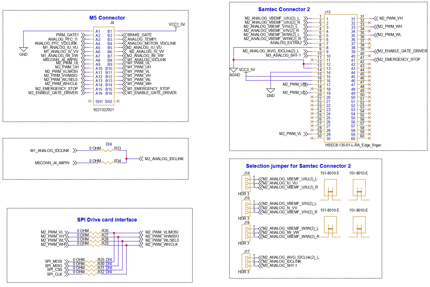
Figure 28.
Drive adapter card expansion headers
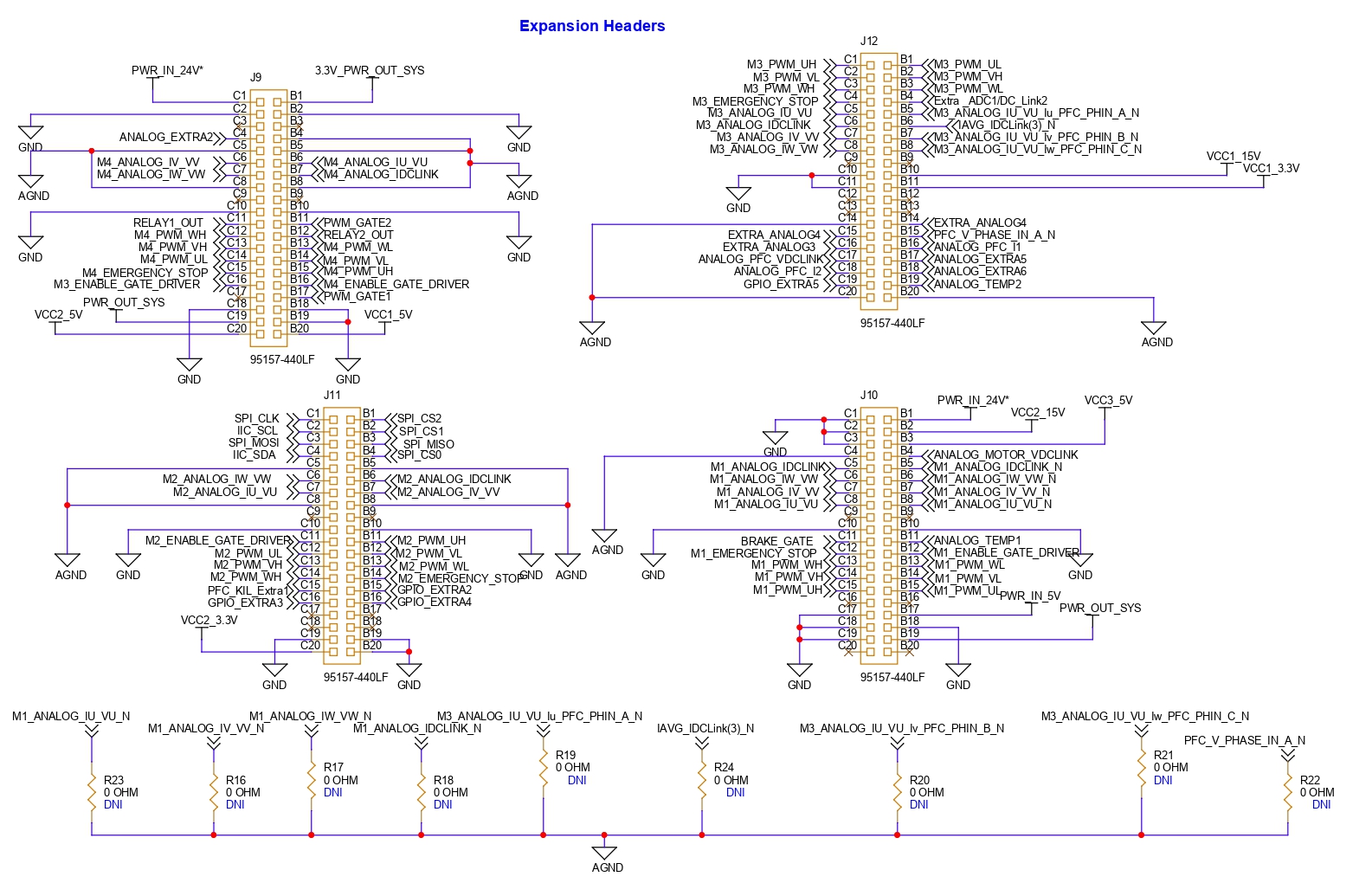
Figure 29.
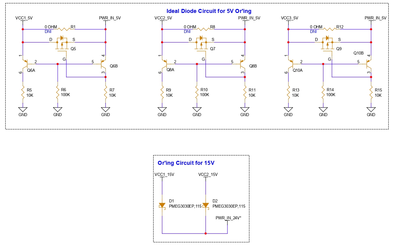
Power supply ORing circuits
1
The AN_A5_VBEMF_U/IU(3) net is connected to pin B45 of the 100-pin high-density connector and is used for PFC current sensing (ANALOG_PFC_I1 signal).
2
The AN_B7_IAVG_IDCLink(3) net is connected to pin A46 of the 100-pin high-density connector and is used for PFC voltage sensing (ANALOG_PFC_VDCLINK signal).
Production data
The KIT_PSC3M5_CC2 control board is designed with Altium, while the drive adapter card is designed in Orcad. The complete PCB design data, schematics, layout, and BOM for this board can be downloaded from the kit
webpage
.
Revision history
Document version | Date of release | Description of changes |
|---|---|---|
** | 2024-09-20 | Initial release |
*A | 2024-12-05 |
|
1
The AN_A5_VBEMF_U/IU(3) net is connected to pin B45 of the 100-pin high-density connector and is used for PFC current sensing (ANALOG_PFC_I1 signal).
2
The AN_B7_IAVG_IDCLink(3) net is connected to pin A46 of the 100-pin high-density connector and is used for PFC voltage sensing (ANALOG_PFC_VDCLINK signal).