KIT_PSC3M5_EVK PSOC™ Control C3M5 Evaluation Kit guide
About this document
Scope and purpose
This document provides a comprehensive understanding of the KIT_PSC3M5_EVK PSOC™ Control C3 Evaluation Kit, which includes kit operation, an out-of-the-box (OOB) example and its operation, and the hardware details of the board.
Intended audience
This document is intended for all embedded developers using the KIT_PSC3M5_EVK PSOC™ Control C3 Evaluation Kit.
Important notice
“Evaluation Boards and Reference Boards” shall mean
products embedded on a printed circuit board (PCB) for demonstration and/or
evaluation purposes, which include, without limitation, demonstration, reference
and evaluation boards, kits and design (collectively referred to as “Reference
Board”).
Environmental conditions have been considered in
the design of the Evaluation Boards and Reference Boards provided by Infineon
Technologies. The design of the Evaluation Boards and Reference Boards has been
tested by Infineon Technologies only as described in this document. The design
is not qualified in terms of safety requirements, manufacturing and operation
over the entire operating temperature range or lifetime.
The Evaluation Boards and Reference Boards provided
by Infineon Technologies are subject to functional testing only under typical
load conditions. Evaluation Boards and Reference Boards are not subject to the
same procedures as regular products regarding returned material analysis (RMA),
process change notification (PCN) and product discontinuation (PD).
Evaluation Boards and Reference Boards are not
commercialized products, and are solely intended for evaluation and testing
purposes. In particular, they shall not be used for reliability testing or
production. The Evaluation Boards and Reference Boards may therefore not comply
with CE or similar standards (including but not limited to the EMC Directive
2004/EC/108 and the EMC Act) and may not fulfill other requirements of the
country in which they are operated by the customer. The customer shall ensure
that all Evaluation Boards and Reference Boards will be handled in a way which
is compliant with the relevant requirements and standards of the country in
which they are operated.
The Evaluation Boards and Reference Boards as well
as the information provided in this document are addressed only to qualified and
skilled technical staff, for laboratory usage, and shall be used and managed
according to the terms and conditions set forth in this document and in other
related documentation supplied with the respective Evaluation Board or Reference
Board.
It is the responsibility of the customer’s
technical departments to evaluate the suitability of the Evaluation Boards and
Reference Boards for the intended application, and to evaluate the completeness
and correctness of the information provided in this document with respect to
such application.
The customer is obliged to ensure that the use of
the Evaluation Boards and Reference Boards does not cause any harm to persons or
third party property.
The Evaluation Boards and Reference Boards and any
information in this document is provided "as is" and Infineon Technologies
disclaims any warranties, express or implied, including but not limited to
warranties of non-infringement of third party rights and implied warranties of
fitness for any purpose, or for merchantability.
Infineon Technologies shall not be responsible for
any damages resulting from the use of the Evaluation Boards and Reference Boards
and/or from any information provided in this document. The customer is obliged
to defend, indemnify and hold Infineon Technologies harmless from and against
any claims or damages arising out of or resulting from any use thereof.
Infineon Technologies reserves the right to modify
this document and/or any information provided herein at any time without further
notice.
Safety precautions
Note:
Please note the following warnings regarding the hazards associated with development systems.
 | Caution: The evaluation or reference board contains parts and
assemblies sensitive to electrostatic discharge (ESD).
Electrostatic control precautions are required when
installing, testing, servicing or repairing the assembly.
Component damage may result if ESD control procedures are
not followed. If you are not familiar with electrostatic
control procedures, refer to the applicable ESD protection
handbooks and guidelines. |
| Caution: The evaluation or reference board is shipped with packing
materials that need to be removed prior to installation.
Failure to remove all packing materials that are unnecessary
for system installation may result in overheating or
abnormal operating conditions. |
Introduction
The PSOC™ Control C3M5 Evaluation Kit enables you to evaluate and develop applications using the PSC3M5 MCU.
PSOC™ Control C3M5 is a high-performance, low-power, 32-bit single-core Arm® Cortex® M33-based MCU running at up to 180 MHz with a digital signal processor (DSP), a floating-point unit (FPU), and state-of-the-art security features.
This device has the following features:
High-performance, programmable analog subsystem (HPPASS):
12-bit, 12-Msps SAR ADC with parallel idle sampling of up to 16 analog channels
Five comparators with <10 ns built-in 10-bit DAC and slope generator
Real-time control peripherals:
Coordinate rotation digital computer (CORDIC)
Sixteen 16-bit and four 32-bit timer/counter pulse-width modulators (TCPWM) supporting <80 ps high-resolution pulse-width modulation (HRPWM)
Enhanced routing flexibility with a combinatorial trigger multiplexing unit
Communication interfaces: Up to six SCB and two CAN FD (one supporting 8 Mbps)
256 KB read-while-write flash with ECC support
Low-power operation modes down to 300 nA: Sleep, Deep Sleep (three modes), and Hibernate
Up to 50 GPIOs with programmable drive modes, strengths, and slew rates; up to 28 pins support Smart I/O programmable logic and up to 16 dedicated analog pins
Security: PSA L2 certified; configurable flash partitioning and protection
Safety: Class B and SIL 2-compliant safety test libraries are available
Power supply range: 1.71 V to 3.63 V
Ambient temperature range: -40°C to 105°C Ta
Packages: VQFN-48, E-LQFP-48, VQFN-64, E-LQFP-64,E-LQFP-80
The evaluation board has two Infineon Shield2Go standard headers (S2GO) and one mikroBUS header for interfacing sensors. It also features headers compatible with Arduino shields.
Additionally, the board has the following features:
Onboard programmer/debugger (KitProg3)
CAN FD transceiver
USB Type-C connector for the USB device interface
Two user LEDs, one potentiometer, and two user buttons
The board operates at 3.3 V
ModusToolbox™ software is used to develop and debug PSC3M5 projects. It is a comprehensive set of tools that enable you to seamlessly integrate these devices into your existing development methodology.
Kit details
This section describes the details of the PSOC™ Control C3M5 Evaluation Kit.
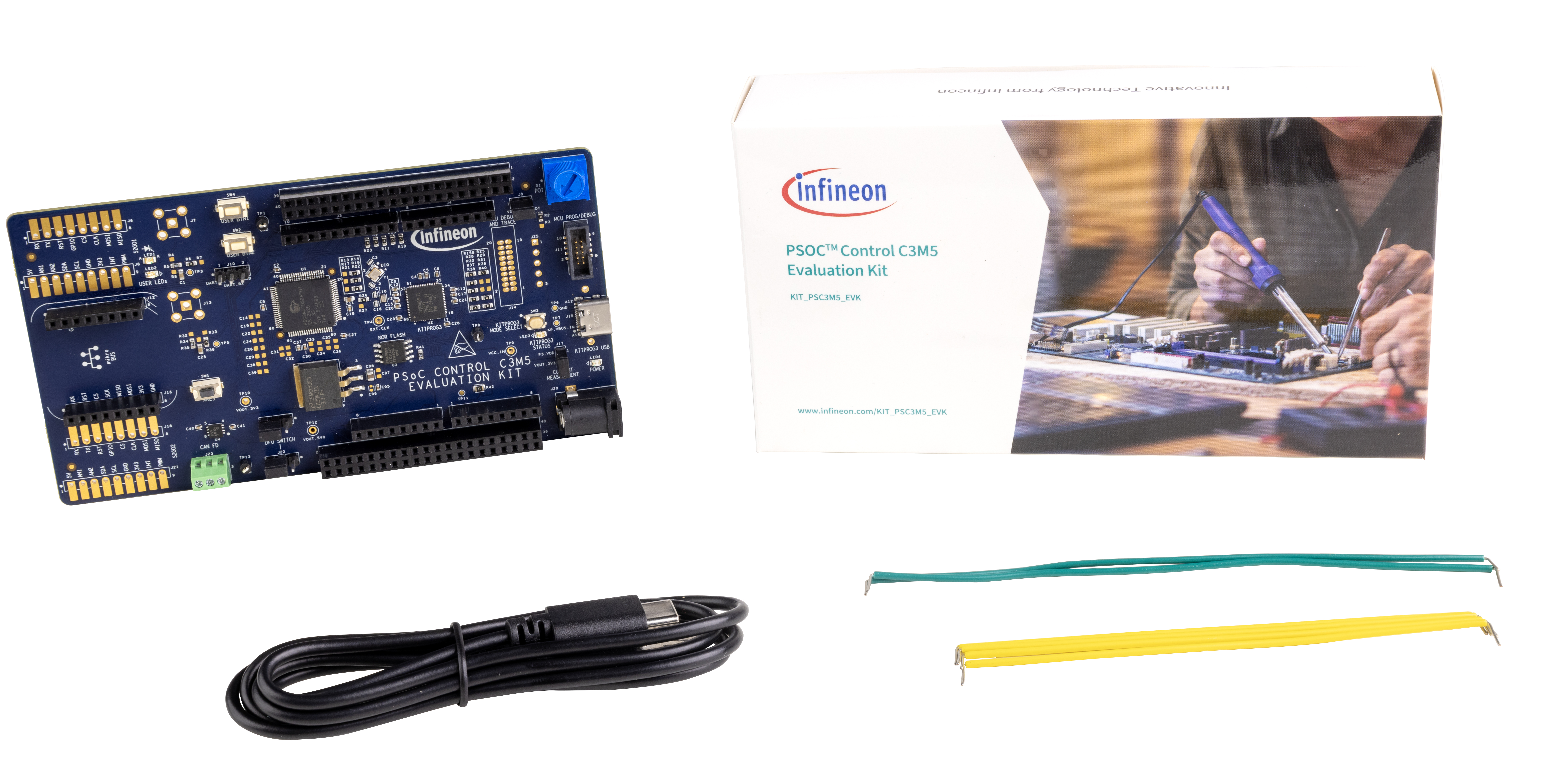
Kit contents
The kit comprises the following components:
PSOC™ Control C3M5 Evaluation Kit
USB Type-A to USB Type-C cable
Jumper wires
Quick start guide (printed on the kit package)
Figure 1. Kit content
Board details
The PSOC™ Control C3M5 Evaluation Kit has the following features:
PSOC™Control C3 MCU–PSC3M5FDS2AFQ1
USB Type-C connector for the USB device interface
CAN FD interface
Two user LEDs, two user buttons, and a reset button for the PSC3M5 MCU
Headers compatible with MIKROE’s mikroBUS shields
Headers compatible with Arduino Uno R3
Headers compatible with Infineon's Shield2Go interface
Mode button and mode LED for KitProg3
Potentiometer that can be used to simulate analog sensor outputs
Two (40-pin) expansion headers
Figure 2. KIT_PSC3M5_EVK board details
No. | KIT_PSC3M5_EVK blocks |
|---|---|
1 | DC jack (J20) |
2 | PSOC™ 5LP KitProg3 MCU (U2) |
3 | Power LED (LED4) |
4 | KitProg status LED (LED3) |
5 | USB Type-C connector (J15) |
6 | KitProg mode switch (SW3) |
7 | ETM header (J14) |
8 | 10-pin SWD header (J11) |
9 | Potentiometer (R1) |
10 | 40-pin expansion header1 (J5) |
11 | Primary UART header (J10) |
12 | User button2 (SW2) |
13 | User button1 (SW4) |
14 | SMA headers (J7, J13) |
15 | User LEDs (LED1, LED2) |
16 | Shield2Go-1 headers (J8, J6) |
17 | mikroBUS headers (J16, J12) |
18 | Shield2Go-2 headers (J18, J21) |
19 | CAN header (J23) |
20 | Reset switch (SW1) |
21 | PSOC™ Control C3 target MCU (U1) |
22 | DFU selection headers (J19, J22) |
23 | Arduino headers (J1, J2, J3, J4) |
24 | 40-pin expansion header2 (J24) |
Pin | Primary onboard function | Secondary onboard function | Connection details |
|---|---|---|---|
XRES | Hardware reset | ||
P0.0 | WCO OUT(Y2) | EXT_CLK | The 32.768 KHz crystal pin can be used as an external clock input. To do so, remove R26 and mount R27. |
P0.1 | WCO IN(Y2) | Expansion header J5.5 as GPIO | The 32.768 KHz crystal pin can also be used as a GPIO. To do so, remove R22 and mount R21. |
P1.0 | ECO IN(Y1) | Expansion header J24.37 as GPIO | The 16 MHz crystal pin can also be used as a GPIO. To do so, remove R18 and mount R17. |
P1.1 | ECO OUT(Y1) | Expansion header J5.7 as GPIO | The 16 MHz crystal pin can also be used as a GPIO. To do so, remove R14 and mount R13. |
P1.2 | TCLK_SWCLK | MCU 10-pin SWD/JTAG interface at J11/20-pin ETM header J14 and KP3 | |
P1.3 | TCLK_SWDIO | MCU 10-pin SWD/JTAG interface at J11/20-pin ETM header J14 and KP3 | |
P2.0 | TCPWM pin on expansion header J24.14 | TDI | To use the pin as a JTAG pin on the J11 header, remove R28 and mount R29. |
P2.1 | TCPWM pin on expansion header J24.11 | TDO | To use the pin as a JTAG pin on the J11 header, remove R30 and mount R31. |
P2.2 | DFU_SW1 | Expansion header J24.10 as GPIO | |
P2.3 | DFU_SW2 | Expansion header J24.9 as GPIO | |
P3.0 | Digital I/O on J4.8, and J5.24 | The signal is multiplexed between PSC3M5, the Arduino-compatible header, and the expansion header. | |
P3.1 | Digital I/O on J6.4, J18.4, and J5.28 | The signal is multiplexed between PSC3M5, the expansion header, and the Shield2Go header. | |
P3.2 | UART_RX_0_MIK on J4.1, J12.3, J6.1, J18.1, and J5.31 | The signal is multiplexed between PSC3M5, the Arduino-compatible header, the mikroBUS header, the S2GO header interface, and the expansion header. | |
P3.3 | UART_TX_0_MIK on J4.2, J12.4, J6.2, J18.2, and J5.29 | The signal is multiplexed between PSC3M5, the Arduino-compatible header, the mikroBUS header, the S2GO header interface, and the expansion header. | |
P4.0 | TCPWM1_EXP on J4.4 and J5.35 | ||
P4.1 | TCPWM1_COMPL_EXP on J4.6 and J5.34 | ||
P4.2 | TCPWM_EXP on J4.7 and J5.33 | ||
P4.3 | TCPWM_COMPL_EXP on J3.2 and J5.32 | ||
P4.4 | P4_4 on J5.36 | ||
P4.5 | P4_5 on J8.8, J21.8, and J5.37 | The signal is multiplexed between PSC3M5, the expansion header, and the Shield2Go header. | |
P4.6 | PERI_HRPWM_2 on J5.8 | ||
P4.7 | PERI_HRPWM_3 on J5.10 | ||
P5.0 | User button input from SW4 and J24.36 | The signal is multiplexed with the expansion header and the user switch. | |
P5.1 | PWM_SHIELD on J12.1, J8.9, J21.9, and J24.12 | The signal is multiplexed between PSC3M5, the mikroBUS header, the S2GO header interface, and the expansion header. | |
P5.2 | CAN_RX1 | GPIO in J24.35 | To use the pin as a GPIO, remove R137 and mount R136. |
P5.3 | CAN_TX1 | GPIO in J24.33 | To use the pin as a GPIO, remove R149 and mount R148. |
P6.0 | UART_CTS_1 on J4.5 and J24.29 | ||
P6.1 | UART_RTS_1 on J4.3 and J24.31 | ||
P6.2 | UART_RX | UART_1_RX_EXP on J24.7 | To use the pin as a GPIO, remove R56 and mount R58. |
P6.3 | UART_TX | UART_1_TX_EXP on J24.5 | To use the pin as a GPIO, remove R63 and mount R65. |
P7.0 | SPI_CLK_ARD on J3.6, J16.4, J6.6, J18.6, and J5.18 | The signal is multiplexed between PSC3M5, the Arduino-compatible header, the mikroBUS header, the S2GO header interface, and the expansion header. | |
P7.1 | SPI_MOSI_ARD on J3.4, J16.6, J6.7, J18.7, and J5.14 | The signal is multiplexed between PSC3M5, the Arduino-compatible header, the mikroBUS header, the S2GO header interface, and the expansion header. | |
P7.2 | SPI_MISO_ARD on J3.5, J16.5, J6.8, J18.8, and J5.20 | The signal is multiplexed between PSC3M5, the Arduino-compatible header, the mikroBUS header, the S2GO header interface, and the expansion header. | |
P7.3 | SPI_CS01_ARD on J3.3, and J5.16 | The signal is multiplexed between PSC3M5, the Arduino-compatible header, and the expansion header. | |
P7.4 | PERI_HRPWM_0 | ETM_TRACE_CLK. GPIO on J5.4/SMA connector J13 | To use as an ETM pin on the J14 header, remove R159 and mount R24. To use as a GPIO, remove R35 and mount R34. To use as an HRPWM output for probing, remove R35 and mount R32. |
P7.5 | PERI_HRPWM_1 | GPIO on J5.6/SMA connector J7 | To use the pin as a GPIO, remove R5 and mount R8. To use the pin as an HRPWM output for probing, remove R5 and mount R4. |
P7.6 | P7_6 on CAN FD STB pins, J3.1, and J5.22 | ||
P7.7 | P7_7 on J12.2 and J24.4 | ||
AN_A0 | AN_A0 | Multiplexed with Arduino J2.1 and expansion header J24.23 | |
AN_A1 | AN_A1 | Multiplexed with Arduino J2.2 and expansion header J24.25 | |
AN_A2 | AN_A2 | Multiplexed with Arduino J2.3 and expansion header J24.27 | |
AN_A3 | AN_A3 | Multiplexed with Arduino J2.4 and expansion header J24.22 | |
AN_A4 | AN_A4 | Multiplexed with Arduino J2.5, J16.1, J8.2, J21.2, and expansion header J24.24 | |
AN_A5 | AN_A5 | Multiplexed with Arduino J2.6, J16.1, J8.3, J21.3, and expansion header J24.26 | |
AN_A6 | AN_A6 | Multiplexed with Arduino J2.7 and expansion header J24.34 | |
AN_A7 | AN_A7 | Expansion header J24.20 | |
AN_B0 | ARD_B0 | Expansion header J24.16 | To use the pin in the expansion header, remove R36 and mount R33. |
AN_B1 | ARD_B1 | Expansion header J24.18 | To use the pin in the expansion header, remove R6 and mount R7. |
AN_B2 | AN_B2 | Expansion header J24.17 | |
AN_B3 | AN_B3 | Expansion header J24.19 | |
AN_B4 | Potentiometer | Expansion header J24.21 | To use the pin in the expansion header, remove R2 and mount R3. |
AN_B5 | AN_B5 | Expansion header J24.28 | |
AN_B6 | AN_B6 | Expansion header J24.30 | |
AN_B7 | AN_B7 | Expansion header J24.32 | Multiplexed with Arduino J2.8 and expansion header J24.32 |
P8.0 | LPCOMP0_INP on J5.19 | ETM_TRACE_D0. SPI_CS_FLASH(U3) | To use the pin as an ETM pin on the J14 header, remove R19 and mount R20. To test with U3, remove R113 and mount R114. |
P8.1 | LPCOMP0_INN on J5.13 | ETM_TRACE_D1. SPI_MOSI_FLASH(U3) | To use the pin as an ETM pin on the J14 header, remove R15 and mount R16. To test with U3, remove R95 and mount R96. |
P8.2 | LPCOMP1_INP on J5.15 | ETM_TRACE_D2. SPI_MISO_FLASH(U3) | To use the pin as an ETM pin on the J14 header, remove R11 and mount R12. To test with U3, remove R104 and mount R105. |
P8.3 | LPCOMP1_INN on J5.17 | ETM_TRACE_D3. SPI_CLK_FLASH(U3) | To use the pin as an ETM pin on the J14 header, remove R9 and mount R10. To test with U3, remove R100 and mount R101. |
P8.4 | User LED2 | Expansion header J24.6 | |
P8.5 | User LED1 | Expansion header J24.8 | |
P9.0 | I2C_SCL with KP3, J3.10, J12.5, J8.5, J21.5, and J5.21 | The signal is multiplexed between PSC3M5, the Arduino-compatible header, the mikroBUS header, the S2GO header interface, and the expansion header. | |
P9.1 | TCPWM2_EXP_MCU on J5.25 | ||
P9.2 | I2C_SDA with KP3, J3.9, J12.6, J8.4, J21.4, and J5.23 | The signal is multiplexed between PSC3M5, the Arduino-compatible header, the mikroBUS header, the S2GO header interface, and the expansion header. | |
P9.3 | TCPWM2_COMPL_EXP_MCU on J24.3 | ||
P9.4 | P9_4 on J6.5, J18.5, and J5.11 | The signal is multiplexed between PSC3M5, the mikroBUS header, the S2GO header interface, and the expansion header. | |
P9.5 | P9_5 on J16.3 and J5.9 | The signal is multiplexed between PSC3M5, the mikroBUS interface, and the expansion header. |
Kit operation
The PSOC™ Control C3M5 Evaluation Kit is built around the PSC3M5 MCU. The following section describes the block diagram and peripherals on the board.
For more information on device features, see the device datasheet.
Figure 3. MCU block diagram
Figure 4. PSOC™ Control C3M5 Evaluation Kit block diagram
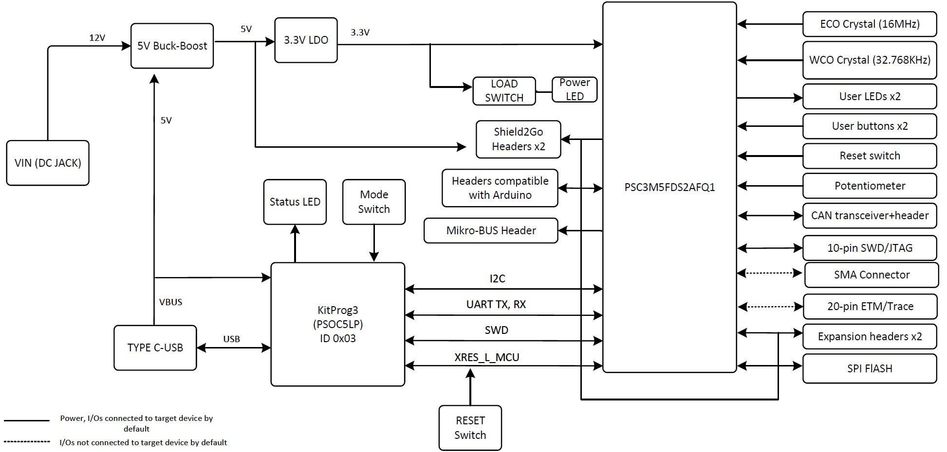
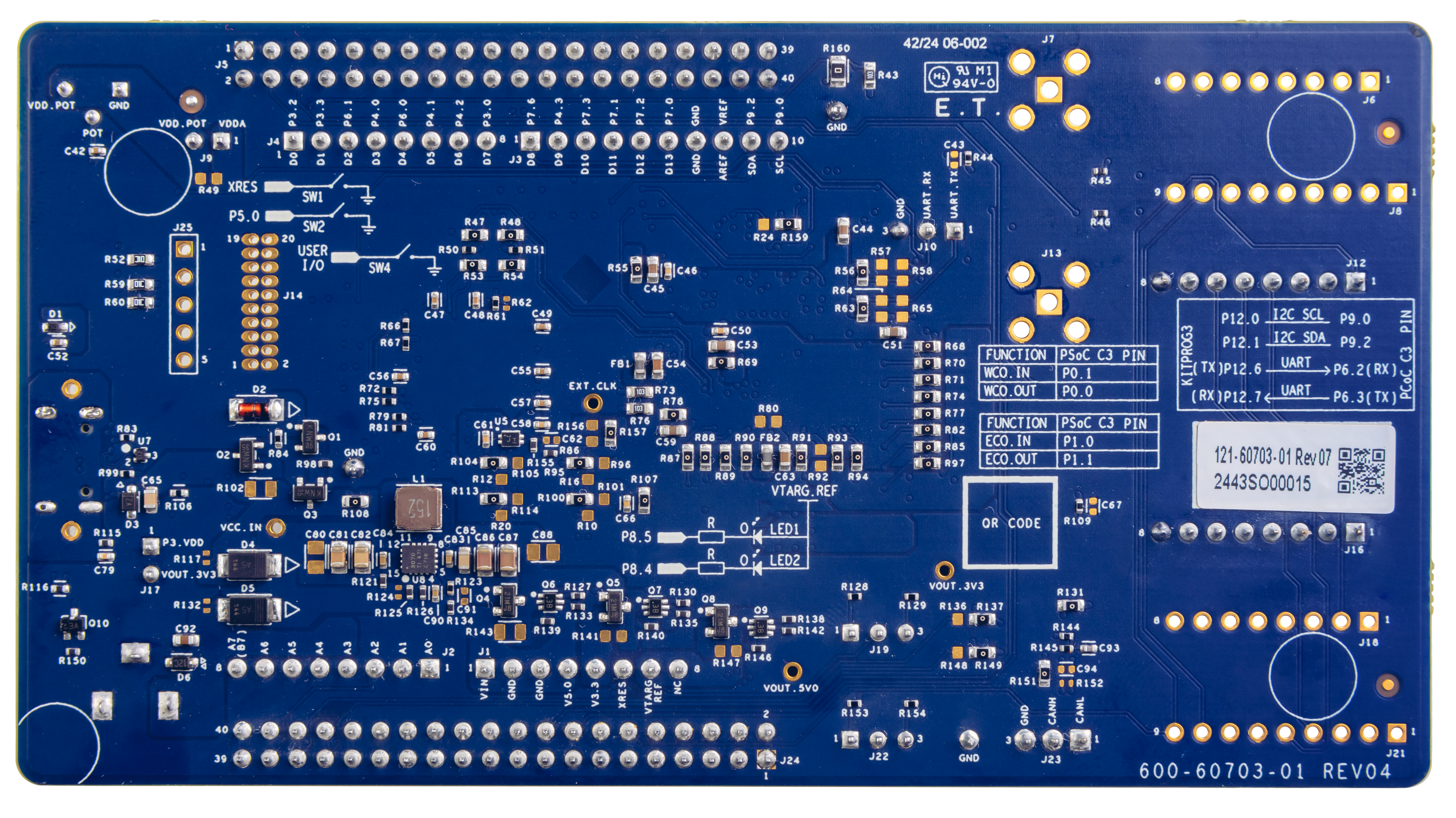
Figure 5. PSOC™ Control C3M5 Evaluation Kit top view
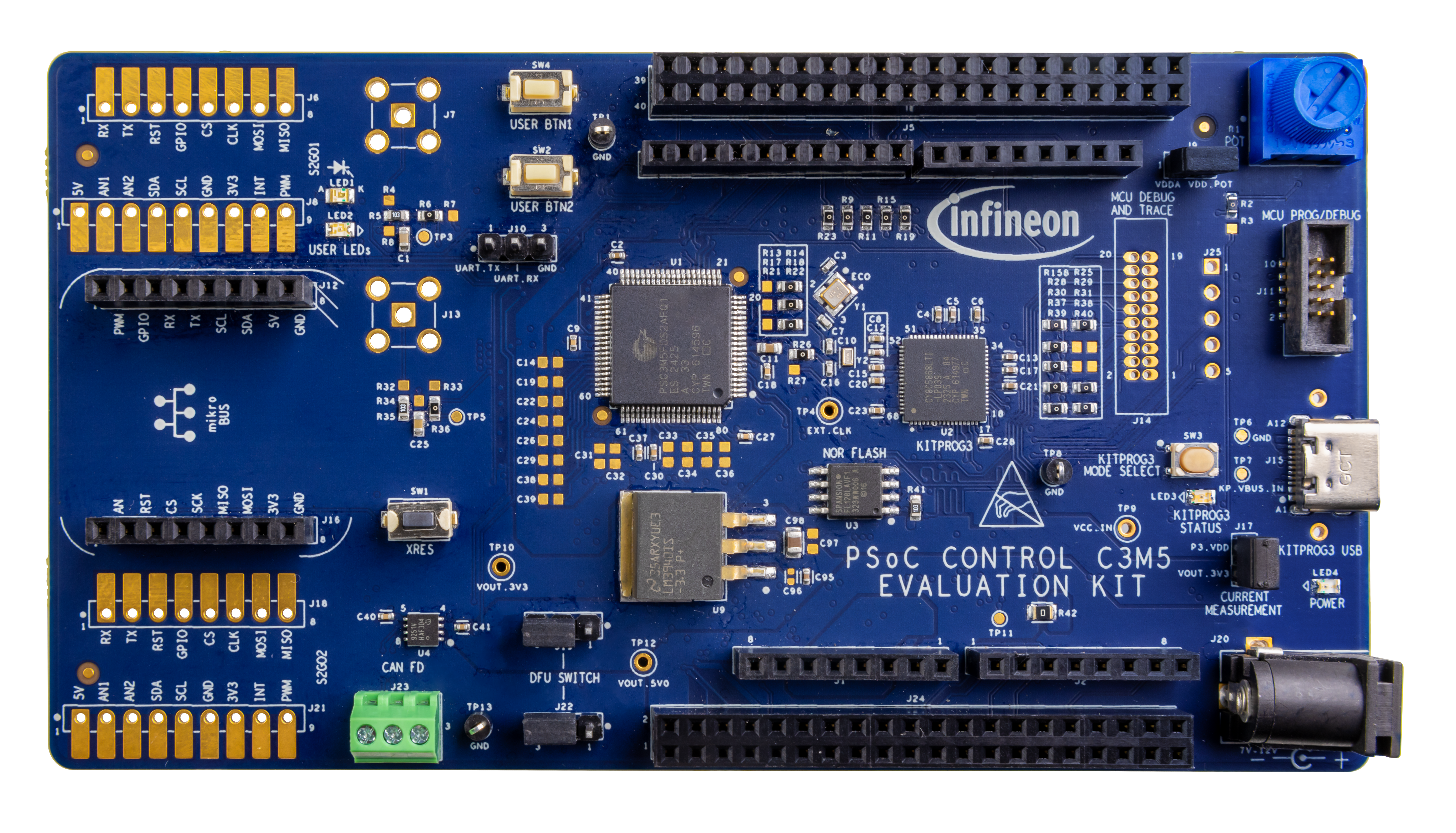
Figure 6. PSOC™ Control C3M5 Evaluation Kit bottom view
The PSOC™ Control C3M5 Evaluation Kit has the following peripherals:
SI. No. | Peripheral | Description |
|---|---|---|
1 | VIN connector | External power supply via a DC jack. A DC adapter with 7 V–12 V and 1 A can be used as a power source for the kit. |
2 | Power LED (LED4) | Power supply ON/OFF LED status indicator. |
3 | KitProg3 USB connector (J15) | Connect to a PC to use the KitProg3 onboard programmer and debugger, and to provide power to the board. |
4 | KitProg3 status LED (LED3) | Indicates the status of KitProg3. For more details, see the KitProg3 user guide. |
5 | KitProg3 programming mode selection button (SW3) | Use this button to switch between various modes of operation of KitProg3. Note that this board supports only CMSIS-DAP BULK mode. For more details, see the KitProg3 user guide. Currently, this button function is reserved for future use. |
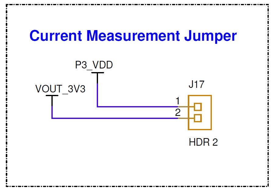
6 | Current measurement jumper (J17) | This jumper enables the user to measure the MCU's current consumption. |
7 | 20-pin debug and trace header (J14) | Connects to an Embedded Trace Macrocell (ETM)-compatible programmer and debugger. |
8 | 10-pin SWD/JTAG program and debug header (J11) | This 10-pin header allows you to program and debug the PSC3M5 using an external programmer, such as the MiniProg4. |
9 | Reset button (SW1) | This button resets the PSC3M5 MCU by connecting the PSC3M5 reset (XRES) pin to ground. |
10 | Potentiometer (R1) | A 10 kΩ potentiometer is connected to the PSC3M5 pin AN_B4. |
11 | Potentiometer connection jumper (J9) | Connects the PSC3M5 VDDA supply to the potentiometer. |
12 | Power header compatible with Arduino Uno R3 (J1) | Power shields compatible with Arduino. It also has a provision to power the kit through the VIN input. |
13 | Analog-IN header compatible with Arduino Uno R3 (J2) | Brings out pins from the PSC3M5 MCU to interface with Arduino-compatible shields. Some of these pins are multiplexed with onboard peripherals and are not connected to the PSC3M5 MCU by default. |
14 | User buttons (SW2, SW4) | Provides an input to the PSC3M5 MCU. Note that, by default, the button connects the PSC3M5 pin to ground when pressed. Therefore, you need to configure the PSC3M5 pin as a digital input with a resistive pull-up to detect the button press. |
15 | User LEDs (LED1 and LED2) | The user LEDs can operate across the entire operating voltage range of the PSC3M5 MCU. The LEDs are active LOW; therefore, the pins must be driven to ground to turn ON the LEDs. |
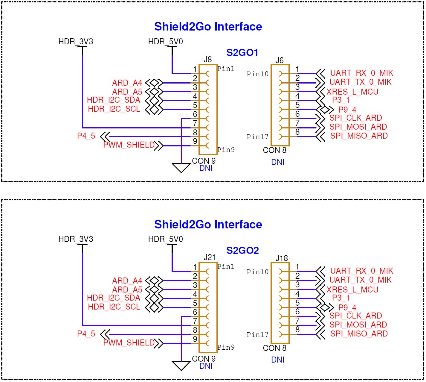
16 | Shield2Go- S2GO21 (J6 and J8) | Infineon’s Shield2Go-compatible header supports sensor functionality working with I 2C, UART, or SPI interfaces. |
17 | Shield2Go-S2GO2 (J18 and J21) | Infineon’s Shield2Go-compatible header supports sensor functionality working with I2C, UART, or SPI interfaces. |
18 | mikroBUS compatible headers (J12 and J16) | MIKROE’s mikroBUS compatible header supports sensor functionality working with I2C, UART, or SPI interface. |
19 | CAN FD interface connector (J23) | This connector is used to connect the kit to the CAN/CAN FD network. |
20 | CAN FD transceiver (TLE9251VLE–U4) | CAN FD transceiver |
21 | Digital I/O headers compatible with Arduino Uno R3 (J3, J4) | Brings out pins from the PSC3M5 MCU to interface with shields compatible with Arduino. Note that some of these pins are multiplexed with onboard peripherals and are not connected to the PSC3M5 by default. |
22 | KitProg3 (PSOC™ 5LP) programmer and debugger (CY8C5868LTI-LP039– U2) | The PSOC™ 5LP device (CY8C5868LTI-LP039) serving as KitProg3 is a multifunctional system that includes an SWD programmer, debugger, USB-I2C bridge, and USB-UART bridge. |
23 | Expansion headers (J5, J24) | This is a 40-pin connector that has all the I/Os mapped from the MCU. Some of these I/Os are connected directly, while others require rework to access. |
24 | DFU headers (J19, J22) | This is a DFU selection header. This I/O is also routed to expansion headers. |
25 | UART header (J10) | This header is used to connect with external UART transceivers, which can communicate with the PSC3M5 MCU. |
26 | PSC3M5 (U1) | Target MCU |
Board support package (BSP) selection
The PSOC™ Control C3 Evaluation Board comes with a KIT_PSC3M5_EVK board support package within the PSOC™ Control BSPs.
To build and run the code examples on the kit, follow the instructions provided in the
Create an application
section of the
ModusToolbox™ user guide
.
KitProg3: Onboard programmer and debugger
The PSOC™ Control C3M5 Evaluation Kit can be programmed and debugged using the onboard KitProg3.
KitProg3 is an onboard programmer/debugger with USB-UART and USB-I
2
C bridge functionality. KitProg3 supports CMSIS-DAP only and does not support mass storage. The PSOC™ 5LP device is used to implement the KitProg3 functionality.
Programming and debugging using the ModusToolbox
Connect the board to the PC using the provided USB cable through a KitProg3 USB connector. If you are connecting it to the PC for the first time, it enumerates as a USB composite device
On this kit, KitProg3 operates in CMSIS-DAP Bulk mode. The status LED (LED4) is always ON in the CMSIS-DAP Bulk mode. If you do not see the desired LED status,see the KitProg3 user guide for details on the KitProg3 status and troubleshooting instructions
In the Eclipse IDE for ModusToolbox™, import the desired code example (application) into a new workspace
Click on New Application from the Quick Panel
Figure 7. Create new application
Select BSP in the Choose Board Support Package window
Figure 8. Board support package in the new application window
Click Next
Select the application in the Select Application window and click Create
Figure 9. Select application window
To build and program an application in the Project Explorer, select a project. In the Quick Panel, scroll to the Launches section and click Program (KitProg3_MiniProg4) configuration
Figure 10. Programming in the ModusToolbox™ IDE
ModusToolbox™ software has an integrated debugger. To debug an application, in the Project Explorer, select the project. In the Quick Panel, scroll to the Launches section and click Debug (KitProg3_MiniProg4) configuration
Figure 11. Debugging in ModusToolbox™ IDE
Using the out-of-the-box (OOB) example – PSOC™ Control C3 MCU: OOB demo
The PSOC™ Control C3M5 Evaluation board comes pre-programmed with the PSOC™ Control C3 MCU's OOB demo code example by default.
The following steps explain how to use the example. For a detailed description of the project, see the following example’s
README.md
file. Once the application is created, check the application directory for the
README.md
file.
Note: At any point in time, if you overwrite the OOB demo example, you can restore it by programming the PSOC™ Control C3 MCU: OOB DEMO.
Connect the board's KitProg3 USB connector to the PC using the provided USB cable
Open a terminal program and select the KitProg3 COM port. Set the serial port parameters to 8N1 and 115200 baud
Press the Reset button (SW1) on the board and confirm that terminal application displays the code example title and other text as shown in Figure 12
Figure 12. OOB demo project message in the terminal
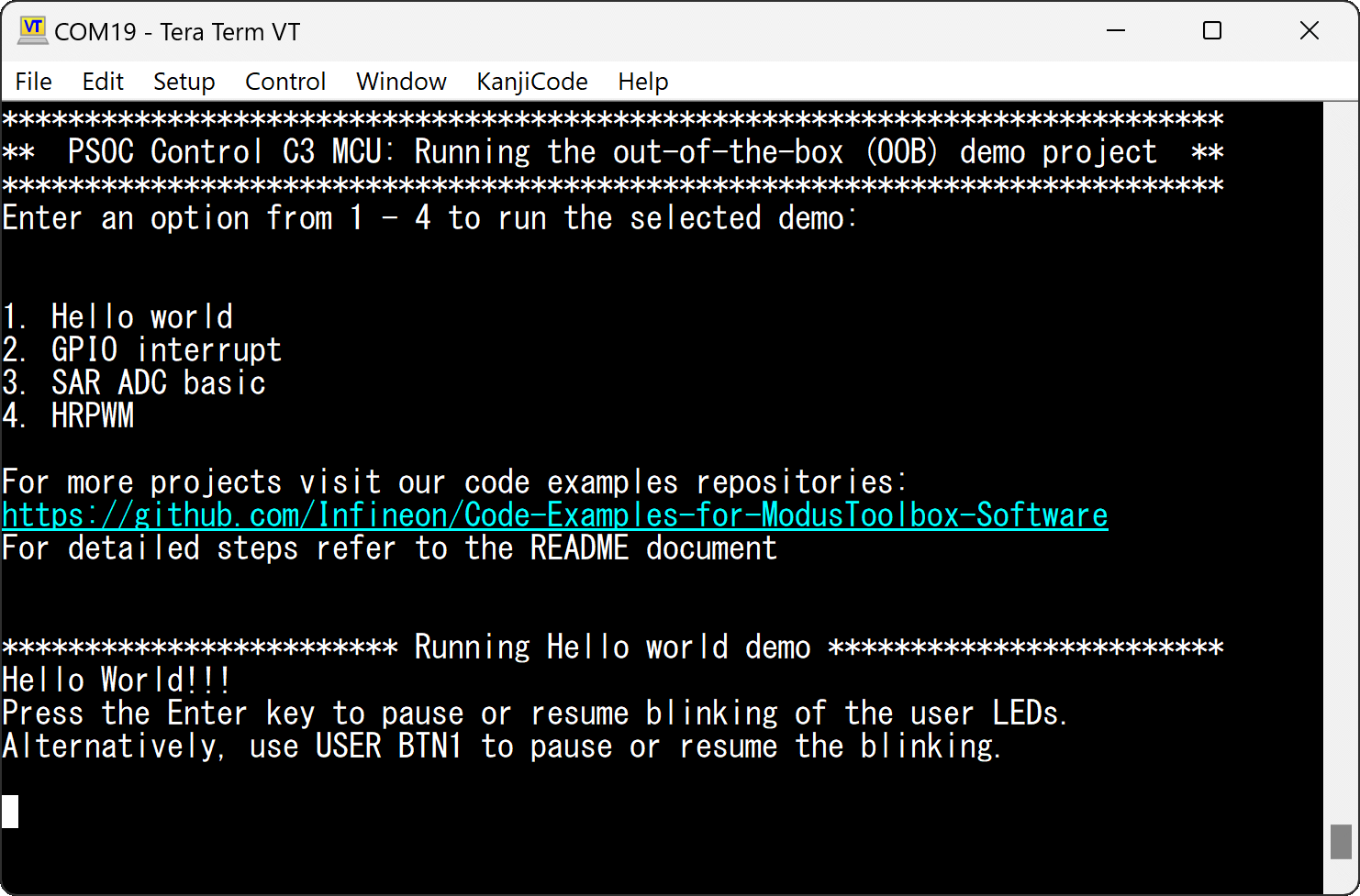
Hello world demo runs by default. Confirm that the kit user LEDs blink sequentially at 1 Hz
Press the
Enter
key; the LEDs (LED1 and LED2) will stop blinking.
The terminal displays the message
LED blinking paused
Repress the
Enter
key; the LEDs (LED1 and LED2) resume blinking at 1 Hz.
The terminal updates the message to
LED blinking resumed
. Alternatively, USER BTN1 can be used to pause or resume the blinking
To run the selected demos, select the options from 1 to 4 as shown in Figure 12 and follow the instructions
Hardware
The following section describes the hardware design.
Schematics
Schematic files are available in the PSOC™ Control C3 M5 Evaluation Kit webpage.
Hardware functional description
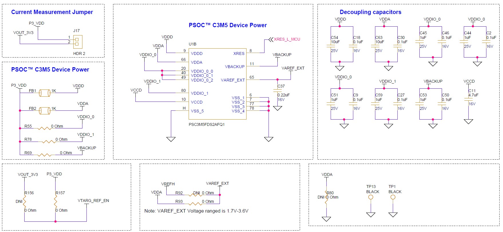
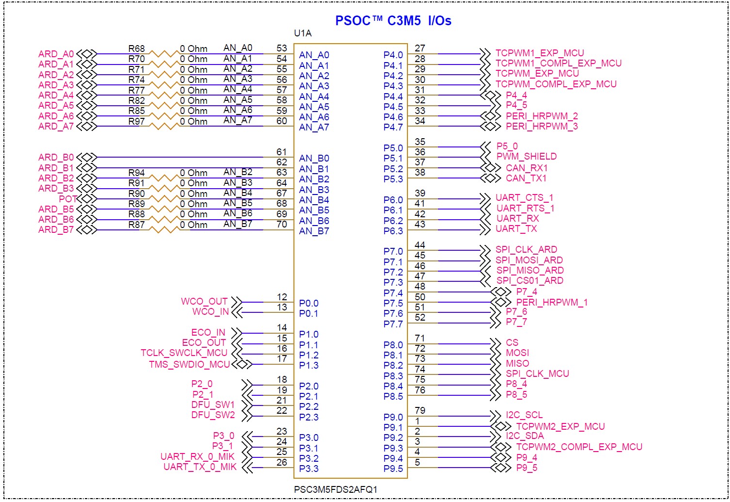
PSC3M5 (U1)
The PSC3P5xD and PSC3M5xD devices are based on the Arm® Cortex®-M33, running at up to 180 MHz with DSP and FPU capabilities. In addition to the CPU subsystem, the devices contain advanced real-time control peripherals, such as a high-performance programmable analog subsystem, comparators, advanced timers with high-resolution capabilities, up to six SCBs, and two CAN FDs for communication.
The devices support one active mode and five low-power modes to manage and reduce power consumption, depending on application requirements.
Figure 13. MCU section
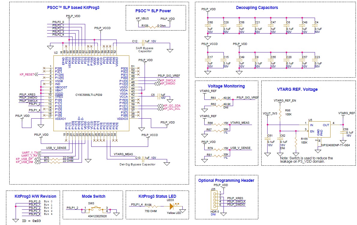
PSOC™ 5LP-based KitProg3 (U2)
An onboard PSOC™ 5LP (CY8C5868LTI-LP039) is used as KitProg3 to program and debug PSC3M5FDS2AFQ1.
The PSOC™ 5LP device connects to the USB port of a PC through a USB connector and to the SWD and other communication interfaces of the PSC3M5FDS2AFQ1.
Visit the PSOC™ 5LP webpage, and for more information, see the CY8C58LPxx family datasheet.
Figure 14. PSOC™ 5LP-based KitProg3 (U2)
Serial interconnection between PSOC™ 5LP and PSC3M5
The PSOC™ 5LP device functions as an interface for USB-UART and USB-I
2
C bridges in addition to being used as an onboard programmer.
The USB-serial pins of the PSOC™ 5LP device are hard-wired to the I
2
C/UART pins of the PSC3M5 device. These pins are also available on the I/O headers compatible with the Arduino Uno.
Figure 15. KP3 serial communication
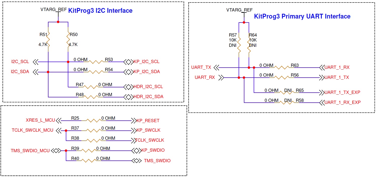
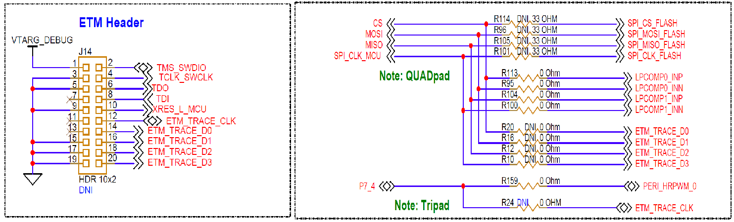
Programming/debugging headers
The PSOC™ Control C3M5 Evaluation Kit is designed with dedicated headers for programming the PSC3M5 device.
A 10-pin SWD/JTAG header (J11) allows you to program the target device using the SWD or JTAG interface. A 20-pin ETM standard header (J14) is provided for trace debugging. Trace output from the PSC3M5 device can be used for debugging purposes.
This 20-pin header is also connected to the SWD and JTAG signals, and this helps a create a single programming header concept for the programming and debugging of the PSC3M5 device.
By default, JTAG debug over the J11 is not enabled. See the following table to rework:
Reference designator | Assembly |
|---|---|
R29 | Stuff |
R31 | Stuff |
R28 | DNI |
R30 | DNI |
By default, TRACE debug over J14 is not enabled. See the following table to rework:
Reference designator | Assembly |
|---|---|
R20 | Stuff |
R16 | Stuff |
R12 | Stuff |
R10 | Stuff |
R24 | Stuff |
R113 | DNI |
R95 | DNI |
R104 | DNI |
R100 | DNI |
R159 | DNI |
Figure 16. Programming headers
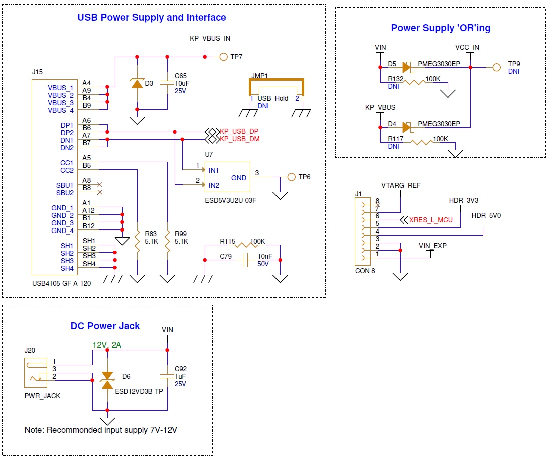
Power supply system
The power supply system on this board is versatile, allowing the input supply to come from the following sources:
5 V from the onboard USB Type-C connector (J15)
7 V–24 V from the external power supply through the VIN barrel jack (J20) or from a (J1) header compatible with Arduino
Figure 17. Power supply input
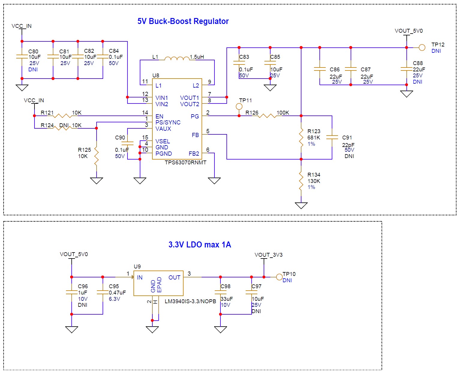
Voltage regulators
The power supply system is designed for the following voltage configurations:
The evaluation kit has two switching regulators:
3.3 V LDO regulator (U9)
3.3 V regulator (U9) output provides the supply to overall peripherals, including the MCU
5 V buck boost regulator (U8)
It is used to power the CAN transceiver and the Arduino headers
Figure 18. Voltage regulator
Current measurement headers
The current of the following domains have dedicated 2-pin headers to facilitate easy current measurement using an ammeter across the pins.
The 2-pin header (J17) is used for checking the MCU current consumption.
Figure 19. Current measurement header
I/O headers
The evaluation kit (EVK) is provided with header interfaces to evaluate sensors and shields with different form factors, such as Arduino, mikroBUS from MIKROE, and Shield2Go from Infineon, which are supported on the EVK.
A few of the I/O signals from the PSC3M5 device are multiplexed by sharing between Arduino, mikroBUS, and the shield2Go headers.
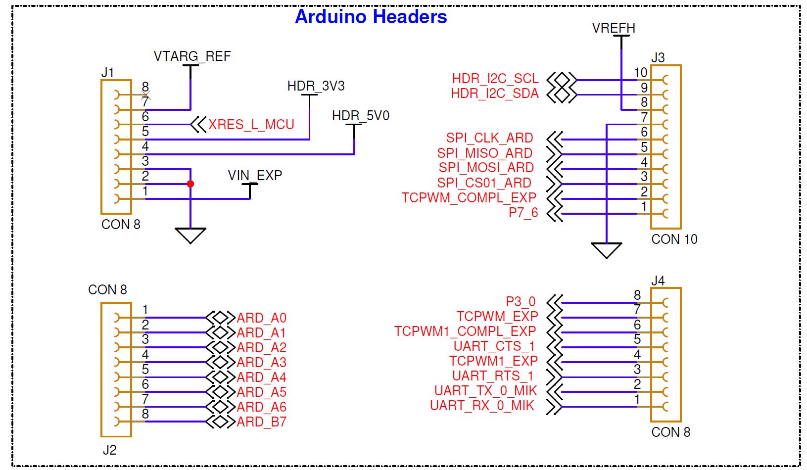
Headers compatible with Arduino Uno R3 (J1, J2, J3, J4)
The board has four headers (J1, J2, J3, and J4) compatible with Arduino Uno R3. Connect 3.3 V or 5 V shields compatible with Arduino Uno R3 to develop applications based on the shield’s hardware.
Note that the kit does not support 5 V and 1.8 V shields.
Figure 20. Arduino headers
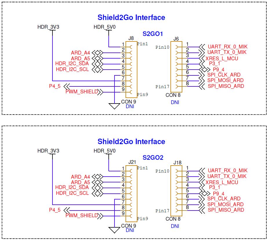
Infineon’s Shield2Go sensor shield compatible headers
The PSOC™ Control C3M5 Evaluation Kit is featured with a footprint compatible to Infineon’s Shield2Go sensor shields.
User can have these shields mounted directly on the board or this can be mounted on headers by having suitable connectors assembled on the board.
Figure 21. Shield2Go compatible headers
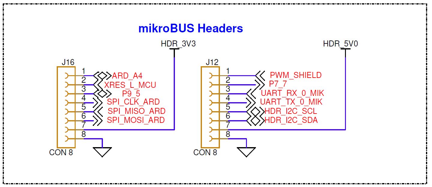
mikroBUS shield compatible headers
The PSOC™ Control C3M5 Evaluation Kit has headers populated to interface with MIKROE standard mikroBUS sensor shields.
You can directly mount the respective mikroBUS sensor shields to evaluate the functionality. The mikroBUS shields are available with different working voltage levels, such as 3.3 V and 5 V. Based on the operating voltage, a shield needs to be selected, and in this kit, only 3.3 V is supported.
Figure 22. mikroBUS headers
I/O expansion headers
The PSOC™ Control C3M5 Evaluation Kit has two expansion headers with 40-pins each, which are J5 and J24.
These headers are made compatible with Infineon's latest motor control lite kit.
Figure 23. I/O expansion headers
CAN FD transceiver
The TLE9251V is a high-speed CAN transceiver, operating as an interface between the CAN controller and the physical bus medium.
A high-speed CAN network is a two-wire, differential network that allows data transmission rates up to 5 Mbps. The CANH and CANL pins are the interfaces to the CAN bus; both pins operate as an input and an output. The RxD and TxD pins are the interfaces to the MCU. The TxD pin is the serial data input from the CAN controller(U4) and the RxD pin is the serial data output from the CAN controller(U4). The voltage level on the digital input TxD and the digital output RxD is determined by the power supply level at the VIO pin. The signal levels on the logic pins (STB, TxD, and RxD) are compatible with MCUs having a 3.3 V I/O supply.
The CAN transceiver will operate accordingly (3.3 V or 5 V).
Figure 24. CAN FD transceiver
LEDs
The evaluation kit (EVK) has four LEDs:
LED3 (Yellow) indicates the status of Kitprog3
LED4 (Red) indicates the power status of the evaluation kit
Two user LEDs (LED1 and LED2) connected directly for user applications
Figure 25. LEDs
Push buttons
The board has the following buttons:
A reset button (SW1) is connected to the XRES pin of the PSC3M5 device and is used to reset the device
One user-controllable buttons (SW2) connected to pin P2.0 of the MCU
One user switch SW4 is connected to P5.0 and can be used to connect any I/O through jumper by removing R160 which can be connected to the J24.38.
A KitProg3 mode selection button (SW3) is connected to the PSOC™ 5LP device for programming mode selection. This button function is reserved for future use (see the KitProg3 user guide for details)
All buttons are in the ACTIVE LOW configuration and short to GND when pressed.
Figure 26. Push buttons
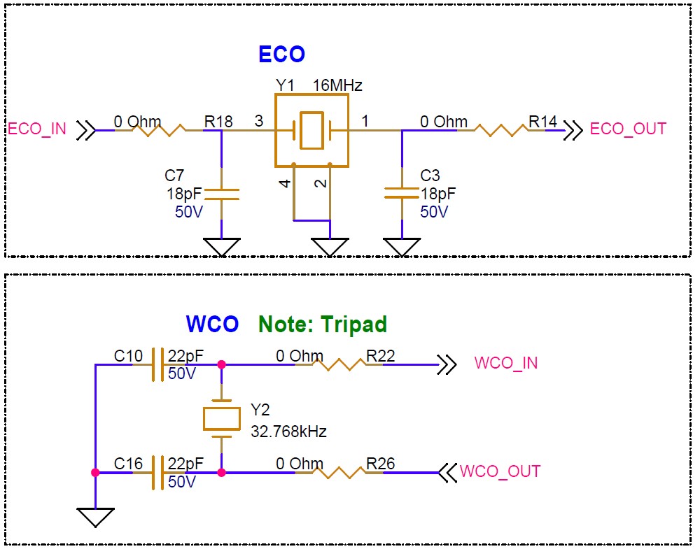
Crystals and oscillators
The evaluation kit has two crystals for clock source:
16 MHz crystal is connected to P1.0 and P1.1 as an External Crystal Oscillator (ECO)
32.768 KHz crystal connected to P0.0 and P0.1 as Watch Crystal Oscillator (WCO)
Figure 27. Crystal oscillator
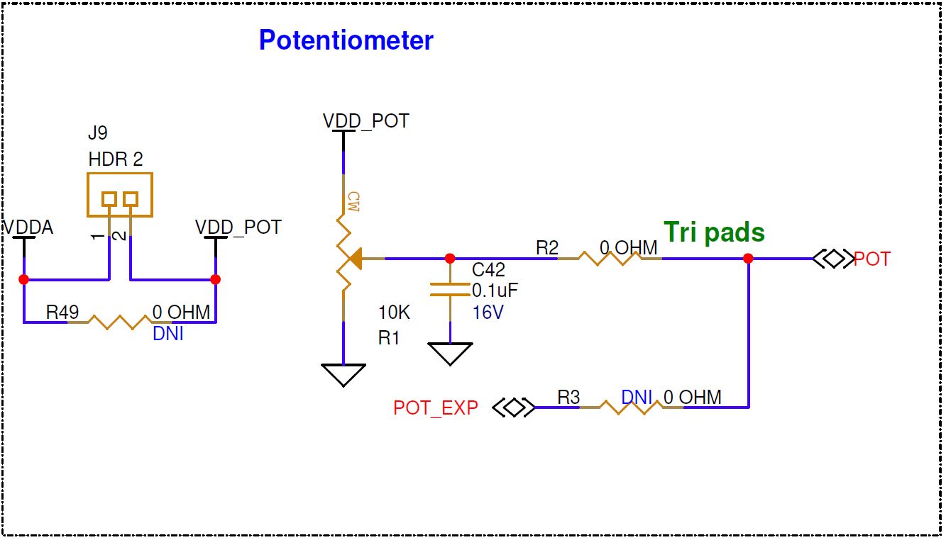
Potentiometer
By default, the board contains a 10K potentiometer connected to AN_B4 pin of MCU.
The same signal is connected to a 40-pin expansion header (J24.21). Remove R2 and mount R3 resistor to isolate the signal from the potentiometer. The fixed ends are connected to VDDA (VDD_POT through J9) and GND which may contribute to leakage current on the P3_VDD supply. Remove the jumper J9 to disconnect power from the potentiometer when measuring the P3_VDD current.
ADC output readings must increase when the potentiometer is rotated in a clockwise direction and conversely.
Figure 28. Potentiometer
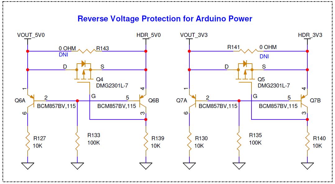
Reverse voltage protection
The following circuit is used to protect the device from reverse supply.
The kit includes a necessary reverse voltage protection circuit to prevent damage from the reverse supply to the board. The circuit protecting the PSC3M5 device will prevent any accidental supply from coming in as input to the board. The board uses a FET-based diode circuit for reverse voltage protection.
The corresponding reverse voltage protection circuit protects the power supply pins from all the headers, such as Arduino, Shield2Go, mikroBUS, and expansion headers. Programming headers are restricted to powering the PSOC™ Control C3 Evaluation Kit. To protect the target device from accidental power fluctuations from the external world, a reverse voltage protection circuit is added to the design.
Figure 29. Reverse voltage protection
Kit rework
The PSOC™ Control C3M5 Evaluation Kit needs to have the following rework to access the peripherals, which are not supported by default.
See
Table 3
for more details.
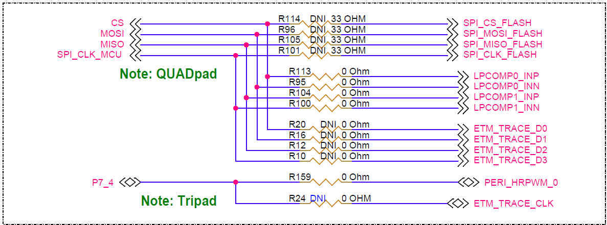
SPI NOR flash
The NOR flash U3 (S25FL128LAGMFV013) is accessible through SCB5 by performing the following rework as shown in
Table 7
.
By default, the SCB5 pins are used as LPCOMP pins, which are routed to the 40-pin expansion headers. To test this memory device (50 MHz), perform the following rework:
Reference designator | Assembly |
|---|---|
R96 | Stuff |
R105 | Stuff |
R101 | Stuff |
R114 | Stuff |
R113 | DNI |
R95 | DNI |
R104 | DNI |
R100 | DNI |
Figure 30. NOR flash
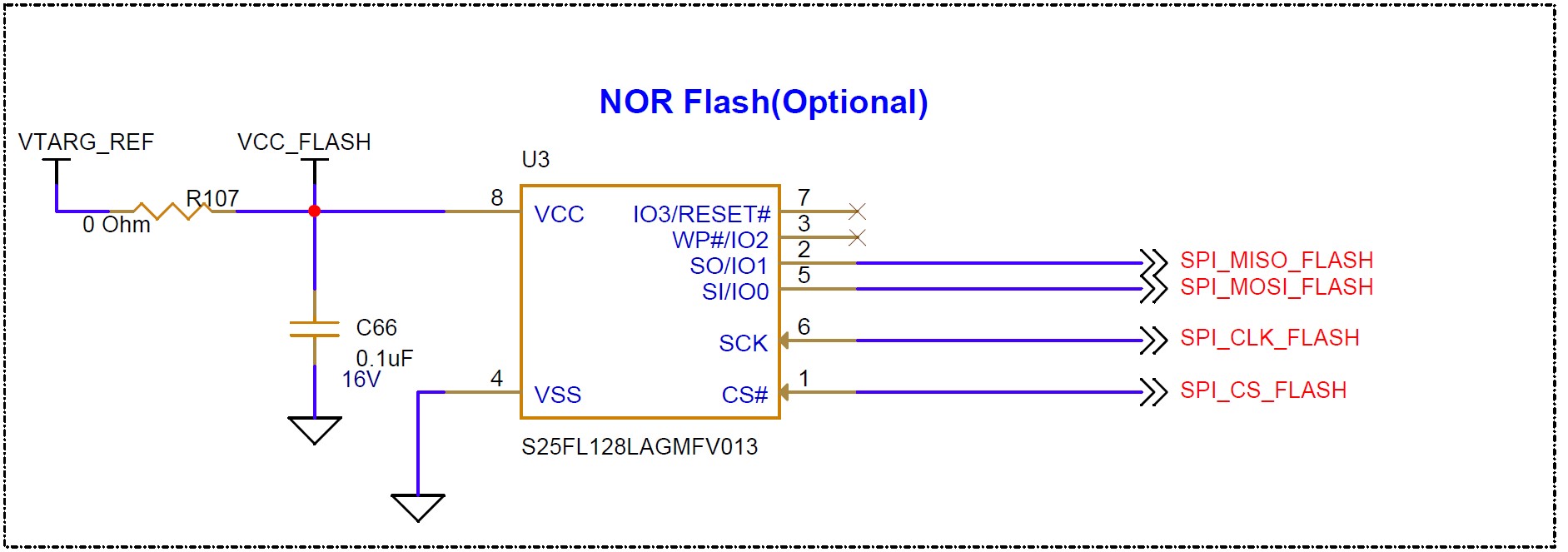
Figure 31. Flash rework
Shield2Go sensor shield assembly
The PSOC™ Control C3M5 Evaluation Kit is featured with a footprint compatible to Infineon’s Shield2go sensor shields. User can have these shields mounted directly on the board or this can be mounted on headers by having suitable connectors assembled on the board.
Note: Infineon’s standard S2GO sensors are voltage tolerant up to 4 V. User should configure the target voltage to 3.3 V (J8, J21) before working with sensor shields on S2GO headers (S2GO1 and S2GO2).
Figure 32. Shield2Go headers
ETM trace and debug header
By default, the ETM trace and debug headers are not populated on the kit. Populate the 20-pin ETM standard connector before using a third-party programmer for trace programming.
Assemble the Trace, JTAG, and SWD respective resistor pins for functional validation of the ETM trace header interface. Mount J14, R20, R16, R12, R10, and R24, and remove R113, R95, R104, R100, and R159 to test this interface.
Figure 33. ETM debug header
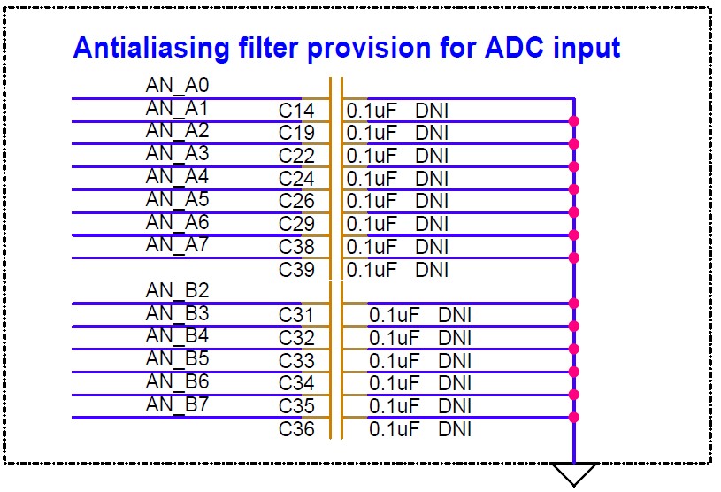
Antialiasing filter for ADC input
To evaluate the ADC pin functionality on the PSOC™ Control C3M5 Evaluation Kit, an antialiasing filter provision is given for analog signals that are connected to J2 of the Arduino compatible header, J16 of the mikroBUS header, and J8 and J21 of the Shield2Go headers and 40-pin expansion header J24.
By default, the PSC3M5 has only default function as an analog series resistor (0 Ω) and an optional capacitor acting as an antialiasing filter. Assemble the necessary capacitors for this operation. To optimize the filtering option, modify the respective resistor value (0 Ω) to a suitable value specific to the user application.
Figure 34. Antialiasing filter capacitors
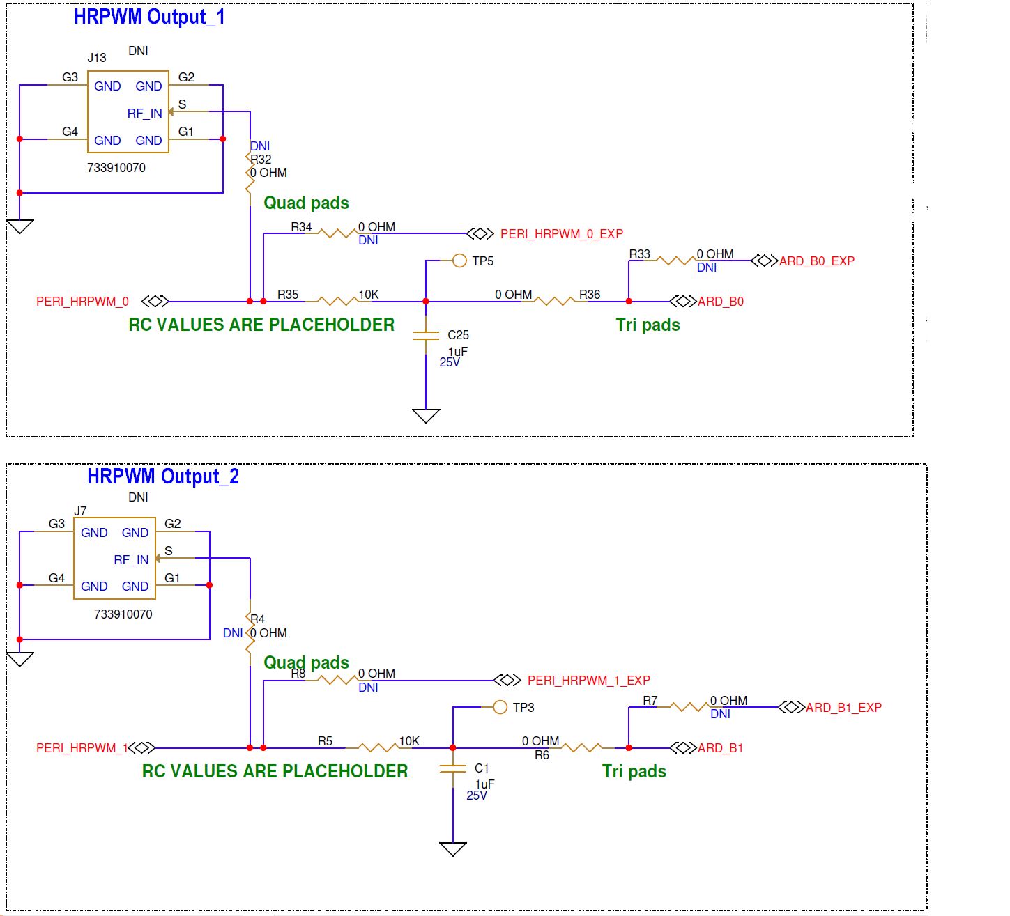
SMA connector (J7, J13)
These connectors are used to probe the HRPWM output from the MCU.
PERI_HRPWM0 and PERI_HRPWM1 are routed to the SMA connector for better measurement of the signal over the oscilloscope. Do the following rework on this test:
Reference designator | Assembly |
|---|---|
R32 | Stuff |
R4 | Stuff |
R35 | DNI |
R5 | DNI |
Figure 35. HRPWM output on SMA connector
Frequently asked questions
Can the evaluation kit be programmed or debugged through the JTAG interface using an external programmer/debugger through a 10-pin SWD/JTAG (J11) header or a 20-pin ETM/Trace header (J14)?
To make the JTAG work using an external programmer/debugger, remove the resistors R28 and R30, and mount R29 and R31
Why is the Deep Sleep current for the PSOC™ Control MCU on the evaluation kit higher due to a leakage path in the MCU power domain?
Before measuring the MCU current, remove the shunt on the J9 header and resistor R115 from the evaluation kit to isolate the leakage path
Why does UART communication using an external USB-UART bridge over header J10 on the evaluation kit not work until the onboard KitProg3 is power cycled by unplugging the USB cable and powering it back on after the external USB-to-UART bridge is connected and powered?
Power the evaluation kit using a DC jack instead of KitProg3 USB power while using an external USB-UART bridge. Note that the onboard KitProg3 programmer and bridge will not work with this setup. Remove resistors R63 and R56, and mount resistors R65 and R58 on the evaluation kit to disable the onboard KitProg3 USB-UART bridge while using an external USB-UART bridge
Revision history
Document revision | Date | Description of changes |
|---|---|---|
** | 2024-05-27 | Initial release |
*A | 2024-12-04 | Updated the following:
|