AN88619 PSOC™ 4 MCU hardware design considerations
About this document
Scope and purpose
This application note shows you how to design a hardware system around a PSOC™ 4 MCU device, starting with considerations for package selection, power, clocking, reset, I/O usage, programming and debugging interfaces, and analog module design.
Intended audience
This document is primarily intended for engineers who need to become familiar with the hardware design principles of PSOC™ 4 MCU devices.
Introduction
PSOC™ 4 is a powerful, programmable microcontroller with an Arm® Cortex®-M0 or Arm® Cortex®-M0+ CPU. It provides the capability and flexibility for analog and digital applications beyond what traditional MCUs offer. Currently, the PSOC™ 4 MCU portfolio contains the following families:
PSOC™ 4000 family: PSOC™ 4000, PSOC™ 4000S, PSOC™ 4000T
PSOC™ 4100 family: PSOC™ 4100, PSOC™ 4100S, PSOC™ 4100S Plus, PSOC™ 4100S Plus 256K, PSOC™ 4100PS, PSOC™ 4100M, PSOC™ 4100L, PSOC™ 4100S Max, PSOC™ 4100BL, PSOC™ 4100T Plus
PSOC™ 4200 family: PSOC™ 4200, PSOC™ 4200M, PSOC™ 4200L, PSOC™ 4200DS, PSOC™ 4200BL
PSOC™ 4500 and PSOC™ 4700 family: PSOC™ 4500S, PSOC™ 4700S
PSOC™ 4 AIROC™ Bluetooth® LE
This application note discusses considerations for hardware design including package, power, clocking, reset, I/O use, programming, and debugging; and provides design tips for analog modules for these device families. It also discusses good board-layout techniques, which are particularly important for precision analog applications.
The PSOC™ 4 MCU device must be configured to work in its hardware environment, which you can do with integrated design environments (IDE) like PSOC™ Creator or ModusToolbox™ IDE; see the “PSOC™ 4 feature set” section of AN79953 – Getting started with PSOC™
4
[1]
to know which IDE is supported for each PSOC™ 4 device. The application note explains various configurations available in PSOC™ Creator and ModusToolbox™ IDE required to set up the device for a given hardware environment.
This application note assumes that you have some basic familiarity with PSOC™ 4 MCU devices, PSOC™ Creator, and ModusTooolbox™ software. If you are new to ModusToolbox™ IDE, see the
ModusToolbox™ software user guide
, which provides a high-level overview of the ModusToolbox™ software. To get started with PSOC™ 4 MCU, see AN79953 – Getting started with PSOC™
4
[1]
. PSOC™ 4 Bluetooth® LE related topics are covered in AN91267 - Getting started with PSOC™ 4 CY8C4xxx-BL MCU with AIROC™ Bluetooth® LE
[16]
. The PSOC™ 4 AIROC™ Bluetooth® LE family has an important topic for hardware design – Bluetooth® LE antenna design. As it involves specific RF expertise, this topic is explored in other application notes. See References
[7]
for more information.
Package selection
One of the first decisions you must make for your PCB is the choice of package. Several considerations drive this decision, including the number of PSOC™ MCU device pins required, PCB and product size, PCB design rules, and thermal and mechanical stability. PSOC™ MCU devices are available in the following packages with different characteristics.
Small-outline integrated circuit (SOIC): This package type is evolved from dual in-line package (DIP). It has two lines of pins and is generally used for chips with a small number of pins (less than 20). Because it has a very large pitch, it is easy to route signals and manually solder. It also provides a good mechanical stability
Thin quad flat package (TQFP): This package type makes it easy to route signals due to the large pitch and the open area below the part. Disadvantages are a larger package size and lower mechanical stability
Shrink small-outline package (SSOP): This package type provides the same advantages and disadvantages as the TQFP package
Quad flat no-lead (QFN): This package type is much smaller than the other packages. The central exposure pad gives the package the best heat dispersion performance and mechanical stability. Disadvantages are that it is more difficult to route signals due to the center pad. For more information, see AN72845 - Design guidelines for Infineon quad flat no-lead (QFN) packaged devices [2]
Wafer level chip-scale package (WLCSP): This package type makes the chip size as small as the die. All pins are led as balls underneath the package. The extremely tiny size of the package makes it a perfect option for the scenarios where the PCB room is critical, such as in portable applications. The disadvantage is that the package provides less mechanical stability than other packages
Very fine-pitch ball grid array (VFBGA): This package type is used for devices with large number of I/Os, as it provides a miniature package for more than hundreds of pins. The disadvantage is a low mechanical stability
As a design reference, see
PSOC™ 4 CAD libraries
, which contain PSOC™ 4 MCU schematics and PCB libraries. Note that you may need to modify the libraries slightly when you use them in your hardware design. Infineon takes no responsibility for issues related to the use of the libraries.
Power
PSOC™ 4 MCU can be powered by a single supply with a wide voltage range, from 1.71 V to 5.5 V. As listed in
Table 1
, it has separate power domains for analog and digital modules. V
DDA
is the analog power supply pin, VSSA is the analog ground pin, V
DDD
and V
CCD
are the digital power supply pins, V
DDIO
is the power supply pin for I/Os, V
SS
is the digital ground pin, and V
DDR
is the RF power pin.
Power domain | Associated pins |
|---|---|
Analog | VDDA, VSSA |
Digital | VDDD, VCCD, VSS |
I/O | VDDIO |
RF | VDDR |
Note:
V
DDIO
is available only in certain device families/packages. I/Os are powered from V
DDD
in devices without a V
DDIO
pin. In some packages, V
DDA
and V
DDD
are combined into a single V
DDD
pin, and V
SSA
and V
SS
are combined into a single V
SS
pin. V
DDR
is available only in PSOC™ 4 AIROC™ Bluetooth® LE family devices. The V
DDR
supply should always be lesser than equal to the applied V
DDD
supply.
Power pin connections
PSOC™ 4 MCU devices can be powered by two modes of power supply: Unregulated external supply and regulated external supply modes. Power pin connections for these two modes are illustrated in
Figure 1
and
Figure 2
.
Unregulated external supply mode
Refer to the device datasheet for the recommended unregulated external supply voltage (V
DD
) range.
In this mode, internal regulators convert the V
DDD
input into the supply voltage for the device digital domain. Output voltage from these internal regulators are also routed to the V
CCD
pin. In such cases, do not power this pin or connect any external load to V
CCD
, except a decoupling capacitor, C
EFC
, indicated in the corresponding device family datasheet and in
Figure 1
.
Also, in this mode, some other internal regulators convert the V
DDR
input into the power supply for the Bluetooth® LE RF transceiver. Note that the regulators for the RF transceiver in a Bluetooth® LE device stop working when V
DDR
is lower than 1.9 V.
Figure 1.
An example of using unregulated external power supply
Note:
For the Bluetooth® LE family, this capacitor is denoted by C
VCCD
in the datasheet.
Regulated external supply mode
You can also power PSOC™ 4 MCU (except the Bluetooth® LE family) with a regulated 1.8-V (±5%) external supply, as
Figure 2
shows. The V
CCD
pins must be tied to the VDDD pin and powered directly with this externally regulated supply. The unused regulators within PSOC™ can be disabled by setting the EXT_VCCD bit in the PWR_CONTROL register to reduce power consumption. For more information, see the PSOC™ 4 MCU
device datasheets
and
reference manuals
.
Figure 2. An example of using regulated external power supply (not applicable for Bluetooth® LE family)
Other power supply considerations
In both modes, connect one 0.1-μF and one ceramic decoupling capacitor, C
EXC
, mentioned in the device datasheet to each power supply pin (note that certain packages have more than one V
DDD
, V
DDA
, and V
DDIO
pin). The PCB trace between the pin and the capacitors should be as short as possible. For more information, see
Appendix B - PCB layout tips
.
Note:
It is a good practice to check a capacitor’s datasheet before you use it, specifically for working voltage and DC bias specifications. With some capacitors, the actual capacitance can decrease considerably when the DC bias is a significant percentage of the rated working voltage.
You can use a single power supply rail for digital power and analog power, which helps to simplify the power design in your board. However, to get a better analog performance in a mixed-signal circuit design, use separate power supply rails for the digital power and the analog power. In all cases, ensure that VDDIO ≤ VDDD ≤ VDDA. For more mixed-signal circuit design techniques, see AN57821 - PSOC™ 3, PSOC™ 4, and PSOC™ 5LP mixed-signal circuit board layout considerations [5].
Proper use and layout of capacitors and ferrite beads help to improve the EMC performance.
The PSOC™ 4 MCU kit webpages (CY8CKIT-040, CY8CKIT-040T, CY8CPROTO-040T, CY8CPROTO-040T-MS, CY8CPROTO-041TP, CY8CKIT-041-41XX, CY8CKIT-042, CY8CKIT-042-BLE, CY8CKIT-043, CY8CKIT-044, CY8CKIT-045S, CY8CKIT-046, CY8CKIT-145, CY8CKIT-147, CY8CKIT-149, CY8CKIT-041S-Max, CY8CKIT-148, and CY8CKIT-148-COIL) provide schematics and bills of material (BOMs) that give good examples of how to incorporate PSOC™ 4 into board schematics. For more information, see
References
.
Power ramp-up (slew rate) considerations
As mentioned previously in Section
Power pin connections
, if you use separate power rails for analog and digital power domains, the voltage at the V
DDA
pin must always be greater than or equal to the voltage at the V
DDD
pin. When PSOC™ 4 MCU is powered up, the voltage at the V
DDA
pin must be present before or at the same time as the voltage at the V
DDD
pin. The maximum allowed voltage ramp rate for any power pin is 67 mV/µs.
Device power settings
Use PSOC™ Creator or Eclipse IDE for ModusToolbox™ software to configure the device power settings
1
. Both the tools use this information to configure the device for optimal performance. If you are using PSOC™ Creator, to open the Design-Wide Resources (DWR) window, double-click the .cydwr file in the project navigator and navigate to the
System
tab to configure the settings as shown in
Figure 3
.
Figure 3.
Device power settings in PSOC™ Creator
In Eclipse IDE for ModusToolbox™ software, open the device configurator to view the
System
tab and select
Power
to configure the device power settings, as
Figure 4
shows.
Figure 4.
Device power settings in device configurator on ModusToolbox™ software
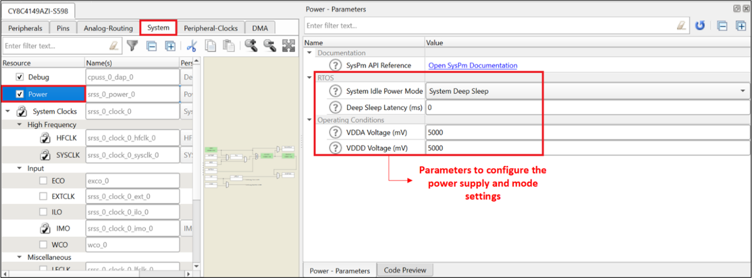
The
Variable VDDA
feature helps the PSOC™ MCU device internal analog routing switch operations by charging pumps when the PSOC™ MCU device analog power supply is low. It is enabled by default when the configured VDDA is lower than or equal to 4.0 V. You can disable it to save power when VDDA exceeds 4.0 V. See the
PSOC™ Creator system reference guide
for more information.
Thermal considerations
Thermal considerations are important in the hardware design processes such as package selection and PCB layout. PSOC™ 4 MCU targets low-power applications, as it consumes no more than 0.2 W. The maximum power consumption is so low that thermal considerations are unnecessary.
Clocking
PSOC™ 4000 / PSOC™ 4000S and PSOC™ 4100 / PSOC™ 4200 / PSOC™ 4100S / PSOC™ 4100PS / PSOC™ 4500S / PSOC™ 4100S Max / PSOC™ 4000T / PSOC™ 4100T Plus have two oscillators: an internal main oscillator (IMO), which drives the high-frequency clock (HFCLK), and an internal low-speed oscillator (ILO), which drives the low-frequency clock (LFCLK). No external crystal is required for IMO and ILO. The IMO is rated at ±2 percent accuracy.
Other than the IMO and ILO, PSOC™ 4100M / PSOC™ 4200M / PSOC™ 4100L / PSOC™ 4200L / PSOC™ 4000S / PSOC™ 4100S / PSOC™ 4100PS / PSOC™ 4100S Max / PSOC™ 4100T Plus provides an additional watch crystal oscillator (WCO), which provides ±50 ppm accuracy. You can hook a 32.768-kHz crystal up to the fixed pins to get an alternative, high-accuracy clock for the LFCLK. Note that the WCO of PSOC™ 4000S / PSOC™ 4100S / PSOC™ 4100PS / PSOC™ 4100S Max devices can’t be a source for LFCLK.
Other than IMO, ILO, and WCO, PSOC™ 4100BLE / PSOC™ 4200BLE / PSOC™ 4100L / PSOC™ 4200L / PSOC™ 4100S Max provides an additional external crystal oscillator (ECO), which provides ±50 ppm accuracy. You can hook a 24-MHz crystal up to the fixed pins to get an alternative, high-accuracy clock for the HFCLK.
A way to get high-accuracy clock for all PSOC™ 4 MCU devices is to bring in a precision clock via the EXT_CLK pin to drive the HFCLK. The external clock’s frequency can be up to 48 MHz. Its duty cycle must be from 45 percent to 55 percent; a square-wave clock is recommended. Check datasheets to get where the EXT_CLK pin is located on different PSOC™ 4 MCU devices.
Clocking settings
You can use PSOC™ Creator or ModusToolbox™ software to manage clocks
2
.
If you are using PSOC™ Creator, you can configure sources and paths for HFCLK and LFCLK that are configurable in two independent sub-tabs (
High Frequency Clocks
and
Low Frequency Clocks
). Switch to
Clocks
tab in the DWR window, and double-click any row in the table of clocks to open the
Configure System Clocks
dialog, as
Figure 5
shows.
Figure 5.
Clock settings in PSOC™ Creator
PSOC™ 4 MCU provides flexible internal clock routing solutions. You can use up to four digital signals in PSOC™ 4 MCU as the routed clock for internal digital logic, which are generally implemented with UDB resources. Select
Topics
in the PSOC™ Creator Help menu and search “Configure System Clocks” to get more information.
In Eclipse IDE for ModusToolbox™ software, the System tab in the device configurator (design.modus) provides the options to configure the clocks.
Figure 6
shows how to configure system clocks using ModusToolbox™ software.
Figure 6.
Clock settings in device configurator on ModusToolbox™ software
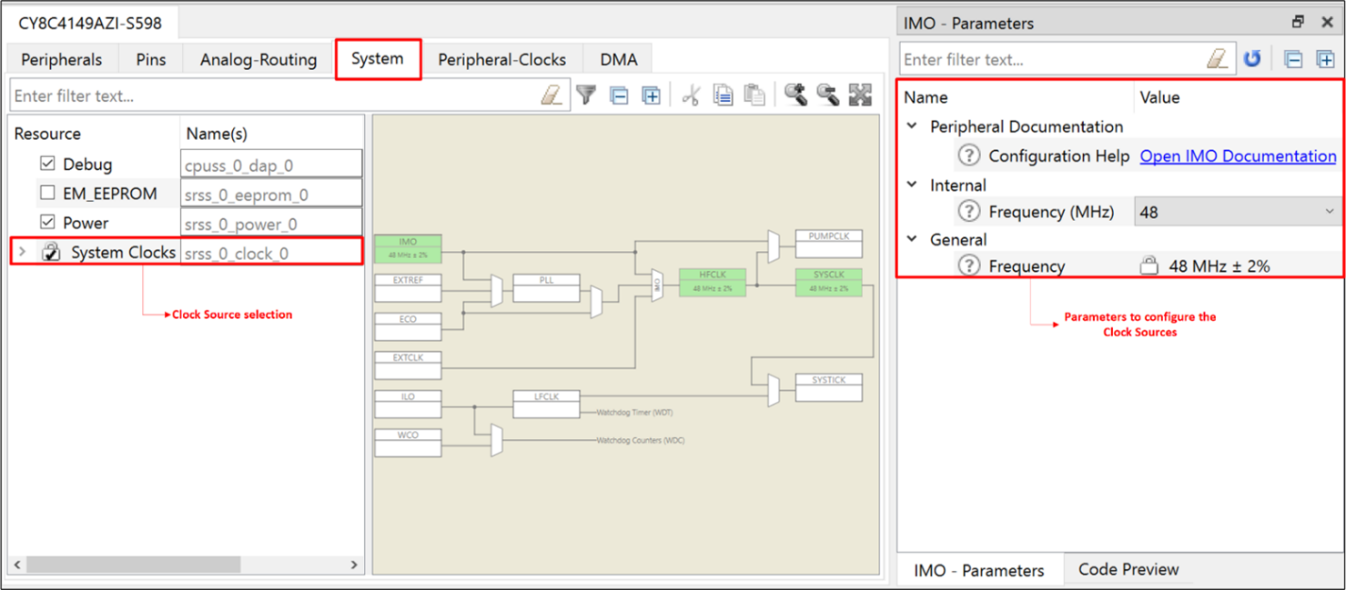
Note:
Unlike PSOC™ 3 and PSOC™ 5LP MCU devices, PSOC™ 4 MCU cannot route the high-frequency clock (HFCLK) directly to any pin owing to its unique internal clock path structure.
2
See “PSOC™ 4 feature set” section of the
AN79953 - Getting started with PSOC™ 4 MCU
application note to know which IDE is supported for each PSOC™ 4 MCU device.
2
See “PSOC™ 4 feature set” section of the
AN79953 - Getting started with PSOC™ 4 MCU
application note to know which IDE is supported for each PSOC™ 4 MCU device.
Reset
The PSOC™ 4 MCU has a reset pin, XRES, which is active LOW. XRES is internally pulled up to VDDD via a resistor called *R
PULLUP
. The value of *R
PULLUP
is specified in the XRES section of the “Electrical Specification” chapter of the device datasheet. If this resistor value is very high, you may need to add an external resistor to XRES for reducing the system startup time.
You can connect a capacitor to the XRES pin, as
Figure 7
shows, to filter out glitches, i.e., any pulses below 50 ns will filter out, thus giving the reset signal better noise immunity. The reset signal requires a pulse-width of at least 5 µs. Typically, a capacitance of 0.1 μF is used in the pin.
Figure 7.
XRES pin connection
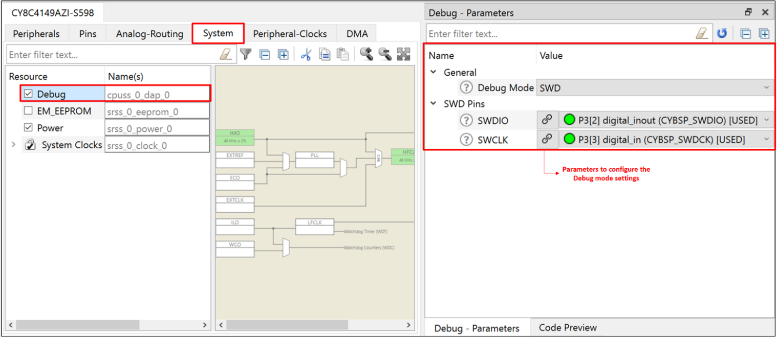
Programming and debugging
PSOC™ 4 MCU supports serial wire debug (SWD) interfaces for device programming and debugging. For programming or debugging, you can use the built-in debugger of PSOC™ 4 MCU kits, or connect PSOC™ 4 MCU to a debugger such as
CY8CKIT-002 PSOC™ MiniProg3 Program and Debug Kit
or
CY8CKIT-005-A MiniProg4 Program and Debug Kit
via a 10-pin or 5-pin connector (see
Figure 8
for pin map). For a 10-pin connector, Samtec FTSH-105-01-L-DV-K (surface mount) or FTSH-105-01-L-D-K (through hole) is recommended. For a 5-pin connector, Molex 22-23-2051 is recommended. Similar parts are available from other vendors.
Figure 8.
SWD connector pin maps for MiniProg3 or MiniProg4
shows the SWD connections.
Figure 9.
SWD connections to PSOC™ 4100/PSOC™ 4200
SWD pins are located in different ports in different device families. The pins could be used for other functionality, when the devices are not being programmed; see the device datasheet for the possible functionality details.
However, if you need to use SWD pins for run-time debugging, in PSOC™ Creator select
SWD (serial wire debug)
, instead of
GPIO
, from the
Debug Select
pull-down list in the
System
tab of the DWR window as
Figure 10
shows. To select the debug port in ModusToolbox™ software, open the device configurator as shown in
Figure 11
. In this case, the pins cannot be used for other functionality any longer.
Figure 10.
PSOC™ Creator debugging settings
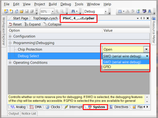
Figure 11.
ModusToolbox™ software debugging settings in the device configurator
Note:
In ModusToolbox™ software, if you need to use SWD pins for other purposes, deselect the debug resource in the
System
tab of the device configurator and configure the pin name and state as required from
Pins
tab.
GPIO pins
PSOC™ 4 MCU provides flexible GPIO pins. Each pin has 4 mA source or 8 mA sink capability. All GPIO pins can be controlled by firmware. Most of them also have alternative connections to PSOC™ 4 MCU peripherals. Different components have different dedicated or fixed pins for their terminals. With dedicated pins, you get the best performance when the peripheral is connected to its own dedicated pin or pins. However, for flexibility, you can connect the peripheral to other pins at the cost of using some internal routing resources.
If a peripheral has fixed pins, then you can connect it to only those pins.
I/O pin selection
When you design a hardware system based on PSOC™ 4 MCU, you should assign the GPIO pins in the following sequence. Note that pins with names in bold may be located at different pins of different ports for different PSOC™ 4 MCU device families; check datasheets for details.
System function pins
SWD: If you need run-time debugging, use the SWD_CLK and SWD_DATA pins
External clock: If you need to use an external clock, use the
EXT_CLK
pin
External 32.768-kHz crystals: for applicable families, if you need a high-accuracy, low-frequency clock, use the
WCO_IN
(or
XTAL32I
) pin and the
WCO_OUT
(or
XTAL32O
) pin
Wakeup: This pin is used to wake up PSOC™ 4 MCU from the Stop low-power mode. If you need this feature, use the
WAKEUP
pin. For more information, see AN86233 - PSOC™ 4 MCU low-power modes and power reduction techniques
[3]
Analog pins
SAR ADC: SARMUX [7:0] pins are used as multichannel inputs to the SAR ADC. In addition, if you want an ADC clock faster than 3 MHz or you need to apply an external reference, reserve VREF for an external bypass capacitor connection. See SAR ADC acquisition time for details.
SARMUX [7:0]
pins are dedicated pins for the SAR ADC. Through the internal analog bus, you can also route signals from the other pins connected to the internal analog bus (See the device datasheet for this information) to the ADC. VREF is a fixed pin for the ADC’s reference bypass capacitor connection
Low-power comparator: PSOC™ 4 MCU has up to two comparators that can work in the Hibernate low-power mode. Each comparator has two fixed pins,
COMPx_INP
(or
LPCOMP.IN_P[x]
) for noninverting input and
COMPx_INN
(or
LPCOMP.IN_P[x]
) for inverting input. Note that PSOC™ 4100S, PSOC™ 4100S Plus, PSOC™ 4100S Plus 256K, PSOC™ 4100 BL, PSOC™ 4100S Max, PSOC™ 4200DS, PSOC™ 4100PS, PSOC™ 4000T, and PSOC™ 4100T Plus do not have the Hibernate low-power mode
Continuous Time Block mini (CTBm): PSOC™ 4 MCU has up to two CTBm modules, each of which is composed of two opamps. One opamp has a dedicated noninverting input pin (
CTBx.OAx.INP
), a fixed inverting input pin (
CTBx.OAx.INN
), and a fixed output pin (
CTBx.OAx.OUT
). If you use an opamp as a comparator, you can route the digital output to a GPIO pin in Port 0, Port 1, Port 2, or Port 3
CAPSENSE™: When you use this module, note that there are two fixed pins. You must connect a reservoir capacitor (C
MOD
) to
CMOD
(or
C_MOD
) pin in all cases, and the other reservoir capacitor (C
SH_TANK
) to
CTANK
(or
C_SH_TANK
) or
CMOD2
pin in some cases. Refer to the relevant device datasheet for information on pin number and capacitor value. You can connect any other pin to a CAPSENSE™ sensor or shield. See AN85951 - PSOC™ 4 and PSOC™ 6 MCU CAPSENSE™ design guide
[5]
for details
Continuous Time Block (CTB): PSOC™ 4100PS has up to two CTB modules, each of which is composed of two opamps and the associated resistor matrix. One opamp has a dedicated noninverting input pin (
CTBx.OAx.INP
), a fixed inverting input pin (
CTBx.OAx.INN
), and a fixed output pin (
CTBx.OAx.OUT
)
Voltage DAC (VDAC): PSOC™ 4100PS has a 13-bit VDAC module that can take input from port pins. The output of VDAC needs to be routed to a port pin through the CTB opamp
Digital pins
Timer/Counter Pulse-Width Modulator (TCPWM): PSOC™ 4 MCU has up to eight TCPWM blocks. Each TCPWM can output two complementary PWM signals. All these signals are routed to dedicated GPIO pins via high-speed paths. See the device datasheet to learn more about these dedicated pins
You can also route these signals via an internal digital connection to other GPIO pins that support digital signal interconnect (DSI). See the respective device datasheet for more details
Serial Communication Block (SCB): PSOC™ 4 MCU has up to four SCBs. Each SCB can be configured as SPI, I
2
C, or UART. Each SCB has fixed pins for its terminals. See the device datasheet to learn more about these pins. Note that PSOC™ 4100PS has up to three SCBs. PSOC™ 4100T Plus has two SCBs with re-configurable I2C, SPI, or UART functionality and three UART blocks with RTS and CTS.
PSOC™ 4000, PSOC™ 4000T, and PSOC™ 4100T Plus can multiplex the SWD and I2C pins on a pair of dedicated GPIO pins, it is useful if running short of GPIOs
Controller Area Network (CAN): PSOC™ 4 MCU has up to two CANs. These have fixed pins for its terminals.
Universal Serial Bus (USB): PSOC™ 4 MCU has fixed pins for USB connectivity. See the respective device datasheet for more details.
Unlike TCPWM, the SCB terminals are routed to fixed pins and cannot be routed to any other GPIO pin. You must follow the fixed pin assignments when using the SCBs.
If your system needs a serial communication interface with a more flexible GPIO pin assignment, you can use a Universal Digital Block (UDB) to implement it in the applicable devices. See the
PSOC™ 4 architecture reference manual
for details
Special ports
In PSOC™ 4 MCU, certain groups of ports have interconnect fabric different from the fabric the other ports have. Therefore, some of the flexible configurations are not available on them. Use the following table as a guideline in the system design. “Y” means the port(s) support the functionality; “N” means the port(s) do not.
PSOC™ 4000 | PSOC™ 4000T | PSOC™ 4000S/4100S | PSOC™ 4100PS | PSOC™ 4100T Plus | PSOC™ 4500S | PSOC™ 4100/4200 | PSOC™ 4100M/4200M | PSOC™ 4100BLE/4200BLE | PSOC™ 4100L/4200L | PSOC™ 4100S Plus | PSOC™ 4100S Max | ||||||
|---|---|---|---|---|---|---|---|---|---|---|---|---|---|---|---|---|---|
Port number | 0, 1, 2 | 3 | 0, 1, 2, 3, 4 | 0, 1, 2, 3, 4 | 0, 1, 2, 3, 4, 5 | 0, 1, 2, 3, 4, 5, 6 | 0, 1, 2, 3, 4, 5, 6, 7 | 0, 1, 2, 3 | 4 | 0, 1, 2, 3 | 4, 5, 6, 7 | 0, 1, 2, 3 | 4, 5 | 0, 1, 2, 3, 4, 5, 10, 11 | 6, 7, 8, 9, 12, 13 | 0, 1, 2, 3, 4, 5, 6, 7 | 0, 1, 2, 3, 4, 5, 6, 7, 8, 9, 10, 11, 12 |
Digital input / output synchronization | N | N | N | N | N | N | N | Y | N | Y | N | Y | N | Y | N | N | N |
Internal digital routing | N | N | N | N | N | N | N | Y | N | Y | N | Y | N | Y | N | N | N |
Internal analog routing | Y | N | Y | Y | Y | Y | Y | Y | Y | Y | Y | Y | Y | Y | Y | Y | Y |
Note:
Digital input/output synchronization:
A digital signal, which input to or output from a PSOC™ 4 MCU pin, can be synchronized to HFCLK. The configurations in PSOC™ Creator are shown in the following figures. Certain port pins, as explained in the section above, do not have this capability. The only valid configuration here is “Transparent”
Internal digital routing
: A digital signal can be routed to a PSOC™ 4 MCU pin with internal digital routing resources. For example, you can route a TCPWM’s output terminals to pins that are not the TCPWM’s dedicated ones. Certain port pins do not have this capability.
Note:
In PSOC™ 4100/PSOC™ 4200 devices, if P4[2] or P4[3] is used to connect CMOD or CSH_TANK, you cannot route a digital output signal to P3[6] or P3[7]
Internal analog routing
: An analog signal can be routed to a PSOC™ 4 MCU pin with internal analog routing resources. For example, you can route an opamp’s input terminals to pins which are not the opamp’s dedicated ones
Figure 12.
GPIO pin output setting
Figure 13.
GPIO pin input setting
Figure 14.
GPIO pin settings in device configurator on ModusToolbox™ software
Component placement
In PSOC™ Creator, you can place Components in different blocks in several ways. For Components with fixed pins, assign the component terminals to the appropriate pin. The following is an example of the UART (SCB mode) Component placement in a PSOC™ 4200 device, where the SCB implements a UART.
In
Figure 15
, there are two pin settings for the UART tx and rx terminals. If you select P4[0] and P4[1], the UART is placed on SCB_0; if you select P0[4] and P0[5], the UART is placed on SCB_1. You can configure these pins in the Pin Editor by clicking the
Pins
tab in the DWR window.
Figure 15.
SCB Component placement by pin selection
Analog Components can be placed using the analog device editor. Click the
Analog
tab in the DWR window to open it.
Figure 16
shows an example of Opamp Component placement
3
.
Right-click the opamp (OAx) to relocate the Component to another available hardware slot. The pins change automatically when the Component is relocated.
The third method to place Components is to use the Directive Editor. Select
Topics
in the PSOC™ Creator Help menu and search “directive” to get more information.
Figure 16.
Opamp Component placement
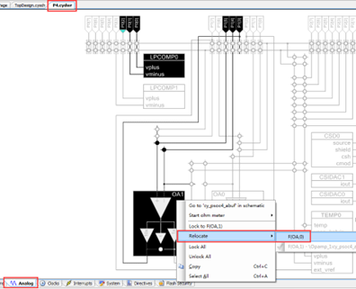
3
The placement details are available only after you build and compile the project, which provides the analog placing and routing details.
Analog module design tips
Analog design is always challenging. Using the PSOC™ 4 MCU analog modules involves several hardware design considerations.
SAR ADC
PSOC™ 4 MCU has up to two unit 12-bit differential SAR ADC, with a sampling rate up to 1 Msps. As mentioned in
I/O pin selection
,
SARMUX [7:0]
pins are dedicated for SAR ADC multichannel inputs They provide the lowest parasitic path resistance and capacitance. You can also route the signals from other pins to the SAR ADC using the internal analog bus, but doing so will introduce high switch resistance (R
SW
in
Figure 19
) and additional parasitic capacitance.
PSOC™ 4 MCU also has an internal precision reference of 1.024 V or 1.2 V
4
(±1 percent). You can use other internal references, including V
DDA
and V
DDA
/ 2, to extend the SAR ADC’s input range. However, note that the accuracy of V
DDA
and V
DDA
/ 2 as references depends on your power system design, and it probably cannot be better than the 1.024 V or 1.2 V precision reference. When you use the internal reference or V
DDA
/ 2 as your reference, a bypass capacitor on VREF pin can help you run the SAR ADC at a faster clock. See
Table 2
for details.
References | Bypass capacitor at VREF pin | Maximum Component clock frequency |
|---|---|---|
Internal 1.024 V/ 1.2 V | Optional | 1.6 MHz |
VDDA / 2 | Optional | 1.6 MHz |
VDDA | Optional | 9 MHz |
Internal 1.024 V/ 1.2 V, bypassed | Mandatory | 18 MHz |
VDDA / 2, bypassed | Mandatory | 18 MHz |
External Vref | Mandatory | 18 MHz |
If you need a reference with a higher accuracy or a specific voltage value, you can connect a custom external reference and a bypass capacitor to the VREF pin.
The SAR ADC is differential physically. When you select Single-ended input mode, you must select the connection for the negative input. There are three options: V
SS
, V
REF
, and an external pin. The SAR ADC’s input range is affected by the selection as well as by the value of the reference voltage. See the chapter “SAR ADC” in the
PSOC™ MCU architecture reference manual
for more information.
You can select the reference and the negative input connection in the
General
tab of the ADC_SAR_SEQ_P4 Component customizer dialog, as
Figure 17
shows.
Figure 17.
SAR ADC reference and negative input settings on PSOC™ Creator
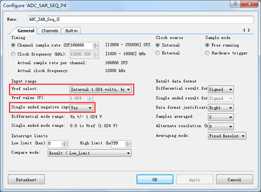
Figure 18.
SAR ADC reference and negative input settings in device configurator on ModusToolbox™ software
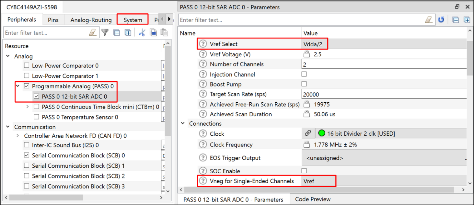
See the respective device datasheet for more details.
SAR ADC acquisition time
Another parameter of concern is the SAR ADC acquisition time, which depends on your hardware design, as
Figure 19
shows.
Figure 19.
Equivalent sample and hold circuit of PSOC™ 4 MCU SAR ADC
V
SRC
is the sampled signal source, and R
SRC
is its output resistance. R
SW
is the resistance of the path from a dedicated pin to the SAR ADC input, which is about 2.2 kΩ. C
HOLD
is the sample and hold capacitance, which is about 10 pF.
shows how C
HOLD
is charged during acquisition time. During acquisition time, the switch in
Figure 19
is ON. Assuming that C
HOLD
is charged from 0, acquisition time is the time required to charge C
HOLD
to a voltage level (V
HOLD
) such that the error (V
SRC
– V
HOLD
) is less than the ADC’s resolution.
Figure 20.
C
HOLD
charging process
If the error is smaller than half the ADC’s resolution (1/2 * LSB), it should be okay. The error can be related to the acquisition time in the following equation:
Here, t
ACQ
is the acquisition time, while is the charging time constant.
PSOC™ 4100/4200 provides a 12-bit differential ADC. If V
REF
is the reference voltage, the resolution can be expressed in the following equation:
This example assumes that the negative input is connected to V
REF
, so that V
SRC
has an input range from 0 to 2 VREF. If the acquisition time is 9 * (RSRC+ RSW) * CHOLD, the error can be expressed as follows:
This equation shows that you should choose an acquisition time that is longer than 9 * (RSRC+ RSW) * CHOLD to make the error less than 1/2 * LSB of the 12-bit ADC. Select the acquisition time in the
Channels
tab of the ADC_SAR_SEQ_P4 Component customizer dialog, as
Figure 21
shows. Note that when you select the number of ADC clocks, the corresponding acquisition time is automatically calculated. See the
ADC_SAR_SEQ_P4 Component datasheet
for details.
In conclusion, pay attention to the output resistance of the sampled signal source, R
SRC
, and the resistance introduced by PCB traces in your ADC hardware design. These determine the acquisition time and therefore the sampling rate.
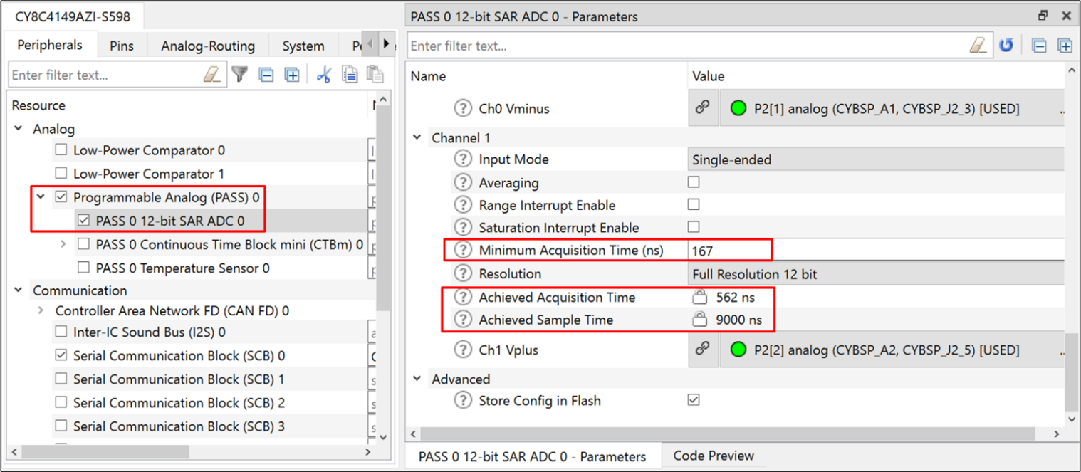
Note:
In ModusToolbox™ software, you can enter the minimum acquisition time for each channel such that is longer than 9 * (RSRC+ RSW) * CHOLD as shown in
Figure 22
and
Figure 23
.
Figure 21.
SAR ADC acquisition time settings on PSOC™ Creator
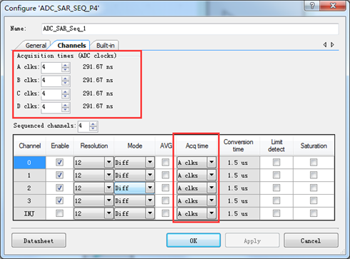
Figure 22.
SAR ADC acquisition time settings for channel 0 in device configurator on ModusToolbox™ software
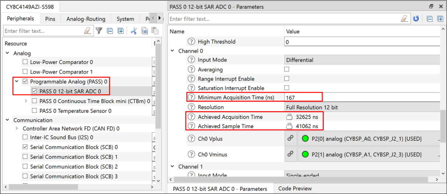
Figure 23.
SAR ADC acquisition time settings for channel 1 in device configurator on ModusToolbox™ software
4
See the chapter “SAR ADC” in the respective PSOC™ 4 MCU device architecture TRM to know the internal bypass reference voltage of that device.
Opamps
The PSOC™ 4 MCU CTBm/CTB provides up to four opamps, which facilitate your analog signal chain design. You can configure each opamp as an amplifier, a follower, or a comparator, as shown
Figure 24
. The PSOC™ 4100PS device CTBscan be configured as programmable gain amplifiers (PGAs) with in-built gain setting resistors.
You can configure the Power mode and output drive capability in the
General
tab of the OpAmp_P4 customizer dialog, as
Figure 24
shows. The opamps have three Power modes. For each Power mode, the opamp has a different input offset voltage, gain bandwidth (GBW) product, and operating current. See the device datasheet for specific values.
You should consider the relation between bandwidth and gain. For example, the highest GBW, 6 MHz, occurs in the High-power/Bandwidth mode. In this case, if the bandwidth of the signal to be amplified is 60 kHz, then the gain cannot be higher than 100 or the amplified signal will be distorted.
If you route an opamp output terminal to a pin for external use, select
Output to pin
for the Output mode. If you route the output terminal for internal use, for example to an input of the SAR ADC, select
Internal only
instead.
Figure 24.
OpAmp_P4 component settings
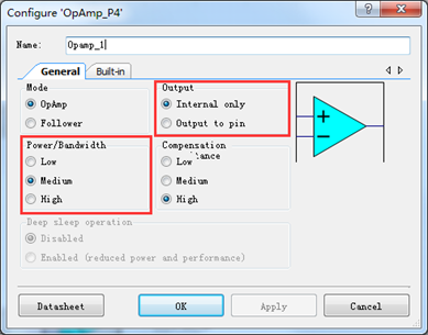
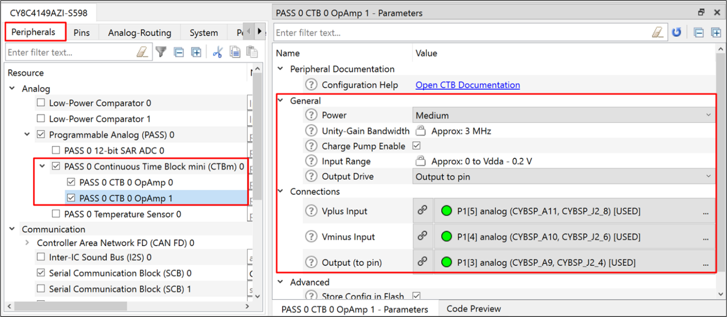
Figure 25.
OpAmp settings in device configurator on ModusToolbox™ software
Comparators
PSOC™ 4 MCU provides as many as six comparators. Four comparators are implemented using the opamps in the CTBm/CTB module, and the other two are the low-power comparators. All comparators' outputs can be routed to PSOC™ 4 MCU UDB resources. This helps you leverage the outputs flexibly. For example, you can invert an output’s logic value. PSOC™ 4 MCU provides three Speed modes for each comparator. For each mode, the comparator has a different output slew rate and operating current. See the device datasheet for specific values.
The low-power comparators can monitor external analog voltage levels in Low-power modes. For more information, see the device datasheets.
When an analog signal’s voltage is divided by a resistor network before it is input into a comparator, take the input resistance of the comparator into account. You can get the comparator’s input resistance from the
device datasheet
.
CAPSENSE
You can connect any PSOC™ 4 pin to a CAPSENSE™ sensor except
CMOD
(or
C_MOD
) pins, which are reserved for C
MOD
5
. When you need to use a shield electrode for waterproofing or proximity features, you may also need to reserve
CTANK
(or
C_SH_TANK
) pin for C
SH_TANK
. If the parasitic capacitance of the shield is less than 200 pF, it is optional to use C
SH_TANK
; otherwise, it is mandatory.
The value for C
MOD
and C
SH_TANK
is usually 2.2 nF. The value may be higher if the parasitic capacitance of the sensors is higher.
In Mutual capacitance sensing mode, you can connect any PSOC™ 4 MCU pin to a CAPSENSE™ Rx/Tx sensor. Two integrating capacitors (C
INT1
and C
INT2
) are required for proper operation. A 470-pF capacitor is recommended on C
INT1
and C
INT2
. For C
MOD
and C
INT
, it is recommended to use temperature compensated and stable dielectric capacitors, for example, C0G (NP0) capacitors.
CAPSENSE™ detects a finger touch by a tiny variation in the sensor’s capacitance (less than 1 pF). It is very sensitive to both signal and noise. Note the PCB layout tips for CAPSENSE™. See AN85951 - PSOC™ 4 and PSOC™ 6 MCU CAPSENSE™ design guide
[5]
for more details.
Pins with a large sink current that are close to CAPSENSE™ pins can introduce an offset to the CAPSENSE™ module’s “GND.”
Figure 26
illustrates a switch circuit for CAPSENSE™ in IDAC source mode. R1 and R2 represent the resistances of PSOC™ 4 internal traces, and R3 represents the resistance of a PCB trace. A shared return path of sink current and CAPSENSE™ current is composed of R2 and R3. The closer a pin with a large sink current is to the CAPSENSE™ pin, the more the sink current that flows through the return path, generating a greater offset.
Figure 26.
Sharing return path
This offset is undesirable and may cause fluctuations in the CAPSENSE™ reading and possible false triggers. Offset compensation can be done in firmware, but it is strongly recommended that you remove the offset in the hardware design instead. Keep pins with a large sink current as far as possible from the CAPSENSE™ pins (best practice is by more than three pins). In addition, pay attention to the return path in your PCB. See AN57821 - PSOC™ 3, PSOC™ 4, and PSOC™ 5LP mixed-signal circuit board layout considerations
[5]
for more details on mixed-signal circuit design.
5
PSOC™ 4100S Max, PSOC™ 4000T, and PSOC™ 4100T Plus have the fifth-generation capacitive sensing method “multi sense converter (MSC)” block, which requires two CMODs for both self-capacitance and Mutual-capacitance sensing modes for each channel, unlike the previous capacitive sensing generations.
Current DACs (IDACs)
PSOC™ 4 MCU provides up to four IDACs: two 8-bit and two 7-bit. See the device datasheet for the electrical specifications. There are two gain options for each IDAC.
Table 3
gives the detailed resolutions and capabilities for each IDAC and gain option.
Step (μA/bit) | 4X Gain | 8X Gain | ||
|---|---|---|---|---|
Output capability (µA) | Step (µA/bit) | Output capability (µA) | ||
8-bit IDAC | 1.2 | 306 | 2.4 | 612 |
7-bit IDAC | 1.2 | 152.4 | 2.4 | 304.8 |
You can set up the IDACs in the Configure tab of the IDAC_P4 Component customizer dialog, as
Figure 27
shows.
Figure 27.
IDAC settings on PSOC™ Creator
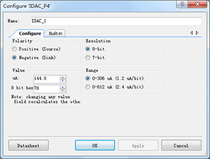
Figure 28.
IDAC settings in Device Configurator on ModusToolbox™ software
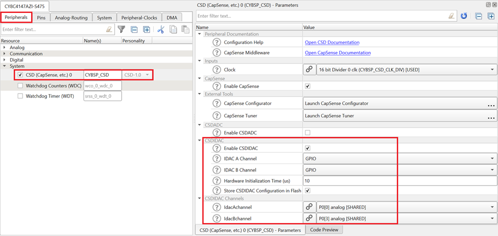
See
CSDIDAC middleware library
for more details.
Through two internal analog buses, you can route IDAC outputs to any two different pins that support analog routing.
Note:
CAPSENSE™ requires one or two IDACs. Ensure that the intended IDACs are not used by CAPSENSE™.
The PSOC™ 4100PS device has programmable voltage reference (PVref) and a 13-bit voltage DAC (VDAC) Components. See
PVref Component datasheet
and
VDAC Component datasheet
for more details on Component parameters.
4
See the chapter “SAR ADC” in the respective PSOC™ 4 MCU device architecture TRM to know the internal bypass reference voltage of that device.
5
PSOC™ 4100S Max, PSOC™ 4000T, and PSOC™ 4100T Plus have the fifth-generation capacitive sensing method “multi sense converter (MSC)” block, which requires two CMODs for both self-capacitance and Mutual-capacitance sensing modes for each channel, unlike the previous capacitive sensing generations.
Summary
PSOC™ 4 MCU provides a flexible solution for designing digital and analog applications. This application note documented the considerations that you need to keep in mind when you build a hardware system around PSOC™ 4 MCU.
Appendix A - Schematic checklist
The answer to each item in the following checklist should be Yes (Y) or Not Applicable (N.A.). For example, if you power a PSOC™ 4 MCU device with an unregulated external supply in your application, you can mark all the items of “Power (regulated external supply)” as N.A.
Catalog | Item | Y/N/N.A. | Remark |
|---|---|---|---|
Power | Is the voltage at the VDDA pin always greater than or equal to the voltages at the VDDD pins? | ||
Is VDDIO ≤ VDDD ≤ VDDA? | |||
Power (unregulated external supply) | Are the power supply pin connections made in accordance with Figure 1 ? | ||
Are the 0.1-μF and 1-μF capacitors connected to each VDDD, VDDIO, VDDA, or VDDR pin? | |||
Are the voltages (including ripples) at the VDDD and VDDA pins in the range of 1.8 V to 5.5 V? | |||
Is the VCCD pin connected to a C EFC capacitor and no other external load? | |||
Is the VCCD pin unconnected with an external supply? | |||
Is the power supply on the VDDR pin higher than 1.9 V. | |||
Power (regulated external supply) | Are the power supply pin connections made in accordance with Figure 2 ? | ||
Are the 0.1-μF and 1-μF ceramic decoupling capacitors connected to each VCCD, VDDD, and VDDA pin? | |||
Are the voltages (including ripples) at the VDDD and VDDA pins in the range of 1.71 V to 1.89 V? | |||
Does your PSOC™ MCU device belong to non-Bluetooth® LE families? | |||
Clocking | Is the external clock connected to EXT_CLK pin? | ||
Is the external clock’s frequency less than or equal to 48 MHz (including tolerance)? | |||
Is the external clock’s duty cycle from 45 percent to 55 percent? | |||
Reset | Is the reset pin connection made in accordance with Figure 8 ? | ||
Programming and debugging | Is the SWD connector’s pin map in accordance with one of the pin maps in Figure 10 or Figure 11 ? | ||
Are the SWD signals connected to SWD_CLK pin and SWD_DATA pin? | |||
Is there a header available to program and debug the PSOC™ 4 MCU using an external programmer? | |||
GPIO pins | Is the assignment of your GPIO pins done in the sequence described in I/O pin selection ? | ||
Is any GPIO pin’s sink current lower than 8 mA? | |||
Is any GPIO pin’s source current lower than 4 mA? | |||
Is the GPIO pins’ total source current or sink current smaller than device capability? | |||
Are port 4, 5, 6, 7 pins used according to Port 4, 5, 6, and 7 GPIO Pins ? | |||
Low-power comparators | Is the assignment of the low-power comparators’ fixed pins in accordance with supported pins? | ||
CTBm | Is the assignment of the CTBm’s fixed pins in accordance with supported pins? | ||
SCB | Is the assignment of the SCB’s fixed pins in accordance with the device datasheet? Are there pull-up resistors connected on the I2C bus? | ||
SAR ADC | Is the connection of the bypass capacitor in accordance with supported pin? | ||
Is the acquisition time of each SAR ADC channel enough to keep the error less than 1/2 LSB? | |||
CAPSENSE™ | Are the pins with strong sink current kept away from the CAPSENSE™ pins (the space is more than three pins)? | ||
Is C MOD 6 connected to CMOD (or C_MOD ) pin? | |||
Is C SH_TANK connected to CTANK (or C_SH_TANK ) pin? | |||
Are the C INT1 and C INT2 7 capacitors connected for mutual capacitive sensing? | |||
Are the CAPSENSE™ sensor, shield, Rx, and Tx signals selected based on recommendations provided in AN85951 - PSOC™ 4 and PSOC™ 6 MCU CAPSENSE™ design guide [15] ? | |||
I2C/UART communication with the host controller | To use I2C/UART communication for tuning the CAPSENSE™ parameters through a host controller, it is recommended to have a header for this interface. | ||
Is there a header available for the above purpose? | |||
IDAC | Is the IDAC not being used by CAPSENSE™? |
6
Two C
MOD
capacitors, C
MOD1
and C
MOD2,
per channel are required in devices with fifth-generation CAPSENSE™.
7
The C
INT
capacitors C
INT1
and C
INT2
are called the C
MOD
capacitors C
MOD1
and C
MOD2
in devices with fifth-generation CAPSENSE™.
Appendix B - PCB layout tips
Note:
Before beginning a PCB layout for PSOC™ MCU, it is a good idea to look at AN57821 - PSOC™ 3, PSOC™ 4, and PSOC™ 5LP mixed-signal circuit board layout considerations
[5]
. Appendix A of that application note shows example PCB layouts and schematics for various PSOC™ packages.
Note:
PSOC™ 3, PSOC™ 4 MCU, and PSOC™ 5LP kit schematics provide good examples of how to incorporate the PSOC™ MCU device into board schematics. For more information, see References.
Note:
For the recommended reflow profile parameters of any Infineon package, please refer to the application note, AN72845 - DESIGN GUIDELINES FOR INFINEON QUAD FLAT NO-LEAD (QFN) PACKAGED DEVICES
[2]
.
There are many classic techniques for designing PCBs for low noise and EMC. Some of these techniques include:
Multiple layers: Although they are more expensive, it is best to use a multilayer PCB with separate layers dedicated to the VSSand VDD supplies. This gives good decoupling and shielding effects. Separate fills on these layers should be provided for VSSA, VSSD, VDDA, VDDIO, and VDDD.
To reduce cost, a two-layer or even a single-layer PCB can be used. In that case, you must have a good layout for all V
SS
and V
DD
.
Ground and power supply: There should be a single point for gathering all ground returns. Avoid ground loops, or minimize their surface area. All component-free surfaces of the PCB should be filled with additional grounding to create a shield, especially when using two-layer or single-layer PCBs.
The power supply should be close to the ground line to minimize the area of the supply loop. The supply loop can act as an antenna and can be a major emitter or receiver of EMI.
Decoupling: The standard decoupler for external power is a 100-µF capacitor. Supplementary 0.1-μF capacitors should be placed as close as possible to the VSS and VDD pins of the device to reduce high-frequency power supply ripple.
Generally, you should decouple all sensitive or noisy signals to improve the EMC performance. Decoupling can be both capacitive and inductive.
Component position: Separate the circuits on the PCB according to their EMI contribution. This will help reduce cross-coupling on the PCB. For example, separate noisy high-current circuits, low-voltage circuits, and digital components.
Signal routing: When designing an application, the following areas should be closely studied to improve the EMC performance:
Noisy signals. For example, signals with fast edge times
Sensitive and high-impedance signals
Signals that capture events, such as interrupts and strobe signals
To improve the EMC performance, keep the trace lengths as short as possible and isolate the traces with V
SS
traces. To avoid crosstalk, do not route them near to or parallel to other noisy and sensitive traces.
For more information, several references are available:
The Circuit Designer's Companion, Second Edition, (EDN Series for Design Engineers), by Tim Williams
PCB Design for Real-World EMI Control (The Springer International Series in Engineering and Computer Science), by Bruce R. Archambeault and James Drewniak
Printed Circuits Handbook (McGraw Hill Handbooks), by Clyde Coombs
EMC and the Printed Circuit Board: Design, Theory, and Layout Made Simple, by Mark I. Montrose
Signal Integrity Issues and Printed Circuit Board Design, by Douglas Brooks
References
AN79953 - Getting started with PSOC™ 4 MCU
AN72845 - Design guidelines for Infineon quad flat no-lead (QFN) packaged devices
AN86233 - PSOC™ 4 MCU low-power modes and power reduction techniques
AN80994 - Design considerations for Electrical Fast Transient (EFT) Immunity
AN57821 - PSOC™ 3, PSOC™ 4, and PSOC™ 5LP mixed-signal circuit board layout considerations
AN91445 - Antenna design and RF layout guidelines
AN91184 - PSOC™ 4 Bluetooth® LE – designing Bluetooth® LE applications
AN95089 - PSOC™ / PRoC Bluetooth® LE crystal oscillator selection and tuning techniques
AN73854 - PSOC™ Creator - Introduction to bootloaders
CY8C4xxx, CYBLxxxx programming specification
PSOC™ 4 application notes
PSOC™ 4 CAD resources
PSOC™ 4 device datasheets
PSOC™ 4 reference manuals
AN85951 - PSOC™ 4 and PSOC™ 6 MCU CAPSENSE™ design guide
AN239751 - Flyback inductive sensing (ISX) design guide
AN91267 - Getting started with PSOC™ 4 CY8C4xxx-BL MCU with AIROC™ Bluetooth® LE
Review the following PSOC™ 4 MCU kit schematics for information on how to incorporate PSOC™ MCU into board schematics.
CY8CKIT-040 PSOC™ 4000 pioneer development kit
CY8CKIT-041-41XX PSOC™ 4100S CAPSENSE™ pioneer kit
CY8CKIT-042 PSOC™ 4 pioneer kit
CY8CKIT-042-BLE-A Bluetooth® Low Energy 5.3 compliant pioneer kit
CY8CKIT-044 PSOC™ 4 M-series pioneer kit
CY8CKIT-043 PSOC™ 4 M-series prototyping kit
CY8CKIT-045S PSOC™ 4500S pioneer kit
CY8CKIT-046 PSOC™ 4 L-series pioneer kit
CY8CKIT-147 PSOC™ 6 Wi-Fi BT prototyping kit
CY8CKIT-149 PSOC™ 4100S Plus prototyping kit
CY8CKIT-041S-MAX PSOC™ 4100S Max pioneer kit
CY8CKIT-148 PSOC™ 4700S Inductive Sensing Evaluation Kit
CY8CKIT-148-COIL Inductive sensing coil breakout board
CY8CKIT-040T PSOC™ 4000T CAPSENSE™ Evaluation Kit
CY8CPROTO-040T PSOC™ 4000T CAPSENSE™ prototyping kit
CY8CPROTO-040T-MS PSOC™ 4000T Multi-Sense prototyping kit
CY8CPROTO-041TP PSOC™ 4100T Plus CAPSENSE™ prototyping kit
Note:
The schematic files of a kit can be found in the PCB design data section in respective kit webpage.
Revision history
Document revision | Date | Description of changes |
|---|---|---|
** | 2014-02-27 | New application note |
*A | 2014-10-07 | Changed the title to “PSOC™ 4100/4200 Hardware Design Considerations - AN88619” to address only PSOC™ 4100/4200 devices Corrected names and links for reference documents Added the latest references Added the link for PSOC™ 4100/4200 SCH and PCB libraries |
*B | 2015-03-25 | Added a table to illustrate the differences between PSOC™ 4100 and PSOC™ 4200 Added TQFP-48 descriptions Added variable VDDA introduction Added routed clock introduction in "Clocking" section Updated PSOC™ Creator Component snapshot per PSOC™ Creator 3.1 |
*C | 2015-05-26 | Updated for PSOC™ 4100M/4200M device Updated template Changed the title |
*D | 2015-10-15 | Updated the descriptions to accommodate all PSOC™ 4 device families Corrected SAR’s clock frequency upper limits under different VREF pin connection scenarios Refreshed the snapshots with PSOC™ Creator 3.2 Corrected the VCCD pin capacitor value from 0.1 μF to 1 μF Clarified that HFCLK connection to pin is not available |
*E | 2016-01-29 | Added self-help section in the beginning of the document. Added PSOC™ 4 L-series information throughout the document. Updated Power Supply Diagram for PSOC™ 4 Bluetooth® LE. Updated Checklist for PSOC™ 4 Bluetooth® LE and the VCCD pin usage. Added Cross References to Bluetooth® LE Documents. |
*F | 2018-03-09 | Updated template Updated for PSOC™ 4100PS device Updated Figure 4 and Figure 5 Updated PSOC™ Resources with PSOC™ 6 references Updated Related Documents with references to AN73854 and Programming specification document |
*G | 2019-05-24 | Updated for PSOC™ 4500 device |
*H | 2020-05-06 | Updated Appendix B. PSOC™ 4100S Plus Flash memory, SRAM and Clocks, and add PSOC™ 4500S Updated PSOC™ 4500 to PSOC™ 4500S |
*I | 2021-09-23 | Updated with the information of PSOC™ 4100S Max device Updated to Infineon template Added ModusToolbox™ software tool details |
*J | 2022-05-12 | Updated for the PSOC™ 4000T device requirements Added “I2C/UART communication with the host controller” in the Schematic checklist section Added footnotes 6 and 7 about the requirement of two Cmod capacitors required for each channel in fifth-generation CAPSENSE™ |
*K | 2022-12-05 | Updated the decoupling and bypass capacitor requirement in Section 3.1. |
*L | 2024-05-31 | Fixed the broken links Added Bluetooth® note in Trademarks section |
*M | 2024-08-01 | Updated the XRES circuit for R PULLUP , Added Reflow Profile recommendation, Updated Appendix A to use C EFC capacitor with VCCD pin |
*N | 2024-08-14 | Updated template |
*O | 2025-01-10 | Updated for New kit CY8CPROTO-040T-MS PSOC™ 4000T Multi-Sense Prototyping Kit |
*P | 2025-03-25 | Template update, Updated for PSOC™ 4100T Plus device |
1
See AN79953 - Getting started with PSOC™ 4 MCU
[1]
to know which IDE is supported for each PSOC™ 4 MCU device.
2
See “PSOC™ 4 feature set” section of the
AN79953 - Getting started with PSOC™ 4 MCU
application note to know which IDE is supported for each PSOC™ 4 MCU device.
3
The placement details are available only after you build and compile the project, which provides the analog placing and routing details.
4
See the chapter “SAR ADC” in the respective PSOC™ 4 MCU device architecture TRM to know the internal bypass reference voltage of that device.
5
PSOC™ 4100S Max, PSOC™ 4000T, and PSOC™ 4100T Plus have the fifth-generation capacitive sensing method “multi sense converter (MSC)” block, which requires two CMODs for both self-capacitance and Mutual-capacitance sensing modes for each channel, unlike the previous capacitive sensing generations.
6
Two C
MOD
capacitors, C
MOD1
and C
MOD2,
per channel are required in devices with fifth-generation CAPSENSE™.
7
The C
INT
capacitors C
INT1
and C
INT2
are called the C
MOD
capacitors C
MOD1
and C
MOD2
in devices with fifth-generation CAPSENSE™.