AN220193 GPIO usage setup in TRAVEO™ T2G family
About this document
Scope and purpose
AN220193 explains how to use GPIO pins effectively in TRAVEO™ T2G family MCUs. This application note also explains GPIO basics, configuration options, interrupts, and low-power behavior.
Intended audience
This document is intended for anyone who uses the TRAVEO™ T2G MCU family.
Associated part family
TRAVEO™ T2G family CYT2/CYT3/CYT4 series
Introduction
TRAVEO™ T2G family MCUs have a flexible general-purpose I/O (GPIO) architecture that provides additional features than traditional MCUs. TRAVEO™ T2G GPIOs are controlled not only by configuring the registers in firmware, similar to traditional MCUs, but are also driven by custom digital logic and analog block signals. This application note explains the basics of TRAVEO™ T2G GPIO pins and shows techniques for using them effectively for different functions. To understand more details about the functionality and terminology used in this application note, see the “I/O System” chapter of the TRAVEO™ T2G architecture technical reference manual (TRM) .
GPIO pin basics
TRAVEO™ T2G GPIO pins offer the following features:
Analog and digital input and output capabilities
Various drive modes
Separate port read and write registers
Slew rate control
High-speed I/O matrix (HSIOM)
Edge-triggered interrupts on rising edge, falling edge, or on both the edges, on all GPIO
Hold mode for latching previous state (used to retain the I/O state in DeepSleep mode)
Selectable CMOS, TTL, and automotive input buffer mode
The GPIO functionality depends on the peripherals available in TRAVEO™ T2G family MCUs.
HSIOM is a set of high-speed multiplexers that route internal CPU and peripheral signals to and from GPIOs. HSIOM allows GPIOs to be shared with multiple functions and multiplexes the pin connection to a peripheral that you select. For details on HSIOM connection, see the architecture TRM .
Physical structure of GPIO pins
Figure 1 shows the pin connections with the resources in TRAVEO™ T2G device.
Figure 1.
Simplified GPIO block diagram
A detailed block diagram of the GPIO structure is available in the I/O system chapter of the architecture TRM . Each pin can act as an input or an output to the digital peripheral such as TCPWM, SCB. Some of the device-specific GPIO can also act as an analog pin for use with ADC. For more details on the analog pins, see the device datasheet . TCPWM provides timers, counters, pulse width modulators, and SCB provides serial communication functions. See the architecture TRM for details of peripheral functions.
At any given time, you can use a pin for digital input, digital output, analog pin, or even combinations of these three. For example, if you enable both digital output and input, it provides a digital bidirectional pin. The input buffer provides high impedance to the external input. It is configurable to CMOS, TTL, and automotive levels. Automotive has a higher threshold level of tripping point than CMOS. See the architecture TRM for different trip levels between CMOS and automotive.
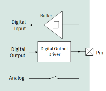
Figure 2 details the digital output driver in Figure 1 . The digital output from each peripheral drives the pin with a digital output driver. The digital output driver supports different drive modes and slew rate control.
Figure 2.
Digital output driver
Slew rate control is provided to reduce EMI and crosstalk and is configured using the SLOW bit of the port output configuration register (GPIO_PRTx_CFG_OUT). There are two options: Fast and slow. Slew rate is set to fast by default. Use the slow option when the signals are not speed critical.
TRAVEO™ T2G device supports various drive modes. Drive mode is configured by the DRIVE_MODE field in the port configuration (GPIO_PRTx_CFG) register. Table 1 lists the supported drive modes, and DRIVE_MODE field setting value. See the architecture TRM for output driver block diagram corresponding to drive modes.
DRIVE_MODE [2:0] field 1 | Drive mode | Application examples |
|---|---|---|
0 | High impedance | Interface to analog and digital input. For digital signals, the input buffer is enabled. For analog signals, the input buffer is typically disabled to reduce crowbar current and leakage in low-power designs. |
2 | Resistive pull-up | Interface to open-drain LOW input, such as the tachometer output from motors or a switch connected to ground. Pins can be used for either digital input or digital output. |
3 | Resistive pull-down | Interface to an open-drain HIGH input or a switch connected to VDD. Pins can be used for either digital input or digital output. |
4 | Open drain, drives low | Provides high impedance in the HIGH state and a strong drive in the LOW state; this configuration is used for I2C pins. This mode works in conjunction with an external pull-up resistor. |
5 | Open drain, drives high | Provides strong drive in the HIGH state and high impedance in the LOW state. This mode works in conjunction with an external pull-down resistor. |
6 | Strong | CMOS output drives in both LOW and HIGH states |
7 | Resistive pull-up and down | Adds a series resistor in both HIGH and LOW states |
Startup and low-power behavior
On reset/power-up, all GPIO pins start up in the high-impedance analog state, that is, with the input buffer and output driver disabled. These GPIO pins remain in this mode until the reset is released. During runtime, GPIOs can be configured by writing to the associated registers.
In Sleep mode, GPIO pins are active and can be actively driven by the peripherals, TCPWM, and SCB; only the CPU is inactive in this mode. In DeepSleep mode, the GPIO pins connected to DeepSleep domain peripherals are functional.
TRAVEO™ T2G MCUs have an additional feature that freezes the GPIOs in DeepSleep and Hibernate modes. The freezing of the GPIO is automatically released, when the device comes out of the low power mode. However, note that the GPIOs driven by DeepSleep peripherals are active in DeepSleep mode and are not frozen.
In the case of Hibernate mode, a device reset wakes up the device. This clears the GPIO configuration and pin state and initializes the GPIO pins to high-impedance analog state. Therefore, GPIO reconfiguration is required.
Interrupt
All port pins have the capability to generate GPIO interrupts. Figure 3 shows GPIO interrupt input block diagram.
Figure 3.
GPIO edge detect block architecture
One GPIO interrupt signal is generated per port. An edge detector is present at each input pin and glitch filter output. The edge detector can detect any of rising-edge, falling-edge, and both edges in the incoming GPIO signal. The glitch filter can be used by one of the pins of a port at a time. Edge detection type is configured by the EDGEx_SEL field in the port interrupt configuration (GPIO_PRTx_INTR_CFG) register. Table 2 lists the supported edge detection types and EDGEx_SEL field values. See the architecture TRM for the output driver block diagram corresponding to drive modes.
EDGEx_SEL field | EDGE type |
|---|---|
0 | Disable |
1 | RISING edge |
2 | FALLING edge |
3 | BOTH edges |
Individual GPIO interrupt signals within a port are ORed together to generate a single interrupt request. Thus, there is one interrupt vector for each port. To determine the port that triggered the interrupt, the GPIO_INTR_CAUSEx registers can be read. The software can read this register to determine the pin(s) or glitch filter signal that caused interrupt activation. The software needs to clear the interrupt cause flags to deactivate the interrupt in the interrupt service routine (ISR).
All I/O pins can be used as wakeup interrupts in Sleep and DeepSleep power mode.
Configuration of GPIO output data
Two types of configurations are available for changing GPIO output data, when GPIO is used as output port:
GPIO_PRTx_OUT
The write register changes the output data to the written data value, and the read reflects the output data setting. Note that the register read does not reflect the current input of I/O pins. You need to use read-modify-write to retain the output data of other pins.
GPIO_PRTx_OUT_CLR and GPIO_PRTx_OUT_SET
These registers can change the output data in the corresponding I/O pins without affecting the output data of other I/O pins. Writing “1” to the GPIO_PRTx_OUT_CLR register clears the corresponding I/O pin to “0”, and writing “0” does not affect the register. Writing “1” to the GPIO_PRTx_OUT_SET register sets the corresponding I/O pin to “1”, and writing “0” does not affect the register.
GPIO settings
This section provides practical examples on the GPIO pins usage and sample register bit settings based on the use case with sample driver library (SDL) provided by Infineon, see Other references . The use cases portrayed in this document are based on CYT2B series. For details on the settings of each series, see the datasheets mentioned in References .
SDL basically has a configuration part and a driver part. The configuration part mainly configures the parameter values for the desired operation. The driver part configures each register based on the parameter values in the configuration part.
You can configure the configuration part according to your system.
Initializing GPIO
Figure 4 shows the flow to initialize the GPIO pin. In this flow, (1) is performed in the configuration part, and (2) to (10) are performed in the driver part. The suffix “y” indicates the pin bit-field within the port register. The detailed settings are described in the use case.
(0) Configure the parameter values according to the system.
(1) Set the initial output state of the GPIO pin to port the output data set register (OUT_SET.OUTy). This is not required if the GPIO pin is set to input.
(2) Configure the HSIOM connection to the pin to the HSIOM port selection register (PORT_SEL0.IOy_SEL). Port becomes active (Port output) by the HSIOM register configuration.
(3) Select the input buffer to port input buffer configuration register (CFG_IN.VTRIP_SELy_0).
(4) Configure the pin output buffer slew rate to the port output buffer configuration (CFG_OUT.SLOWy).
(5) Configure the output drive strength to the port output buffer configuration (CFG_OUT.DRIVE_SELy).
(6) Configure the drive mode to the port configuration register (CFG.DRIVE_MODE3).
(7) Select the disable or enable interrupt to the port interrupt configuration register (INTR_CFG.EDGEy_SEL).
(8) Clear the pin interrupt to the port interrupt status register (INTR.EDGEy).
(9) Configure the interrupt mask to the port interrupt mask register (INTR_MASK.EDGEy).
Figure 4.
GPIO pin initialization procedure
Example code to initialize GPIO in driver part
Code Listing 1 demonstrates an example program to initialize GPIO for writing port level in driver part.
The following description will help you understand the register notation of the driver part of SDL:
basesignifies the pointer to the port register base address.pinNumindicates the pin number within the port register.base->unOUT_CLR.u32Register is the GPIO_PRTx_OUT_CLR register mentioned in the register TRM . “x” signifies the GPIO pin’s port number.
portAddrHSIOM->unPORT_SEL0.u32Register is the HSIOM_PRTx_PORT_SEL0 register mentioned in the register TRM . Other registers are also described in the same manner.
To improve the register setting performance, the SDL writes a complete 32-bit data to the register. Each bit field is generated and written to the register as the final 32-bit data.
tempReg = base->unCFG_IN.u32Register &
      ~(CY_GPIO_CFG_IN_VTRIP_SEL_MASK << pinNum);
      base->unCFG_IN.u32Register = tempReg |
      ((value & CY_GPIO_CFG_IN_VTRIP_SEL_MASK) << pinNum);
See cyip_gpio_v2.h under hdr/rev_x/ip for more information on the union and structure representation of registers.
Code Listing 1 Example for initializing GPIO in driver part
cy_en_gpio_status_t Cy_GPIO_Pin_Init(volatile stc_GPIO_PRT_t *base, uint32_t pinNum, const cy_stc_gpio_pin_config_t *config)
{
    cy_en_gpio_status_t status = CY_GPIO_SUCCESS;

    if((NULL != base) && (NULL != config))
    {
        /* (1) Set port output level */
        Cy_GPIO_Write(base, pinNum, config->outVal);
        /* (2) Configure HSIOM */
        Cy_GPIO_SetHSIOM(base, pinNum, config->hsiom);
        /* (3) Configure input buffer voltage trip type */
        Cy_GPIO_SetVtrip(base, pinNum, config->vtrip);
        /* (4) Set output buffer slew rate */
        Cy_GPIO_SetSlewRate(base, pinNum, config->slewRate);
        /* (5) Configure drive strength */
        Cy_GPIO_SetDriveSel(base, pinNum, config->driveSel);
        /* (6) Configure drive Mode */
        Cy_GPIO_SetDrivemode(base, pinNum, config->driveMode);
        /* (7) Configure interrupt edge */
        Cy_GPIO_SetInterruptEdge(base, pinNum, config->intEdge);
        /* (8) Clear pin interrupt */
        Cy_GPIO_ClearInterrupt(base, pinNum);
        /* (9) Configure interrupt Mask */
        Cy_GPIO_SetInterruptMask(base, pinNum, config->intMask);
    }
    else
    {
        status = CY_GPIO_BAD_PARAM;
    }

    return(status);
}
Following steps break down the configurations of Code Listing 1 .
Set port output level.
Code Listing 2 Setting port output level
__STATIC_INLINE void Cy_GPIO_Write(volatile stc_GPIO_PRT_t* base, uint32_t pinNum, uint32_t value)
{
    /* Thread-safe: Directly access the pin registers instead of base->OUT */
    if(CY_GPIO_ZERO == value)
    {
        /* If value is ‘0’, output state at OUT_CLR.OUT is set to ‘0’. */
        base->unOUT_CLR.u32Register = CY_GPIO_OUT_MASK << pinNum;
    }
    else
    {
        /* If value is ‘1’, output state at OUT_SET.OUT is set to ‘1’. */
        base->unOUT_SET.u32Register = CY_GPIO_OUT_MASK << pinNum;
    }
}
Configure HSIOM.
Code Listing 3 Configuring HSIOM
__STATIC_INLINE void Cy_GPIO_SetHSIOM(volatile stc_GPIO_PRT_t* base, uint32_t pinNum, en_hsiom_sel_t value)
{
    uint8_t  pinNumForHsiom;
    uint32_t portNum;
    uint32_t tempReg;
    stc_HSIOM_PRT_t* portAddrHSIOM;

    portNum = ((uint32_t)(base) - GPIO_BASE) / GPIO_PRT_SECTION_SIZE;
    portAddrHSIOM = (stc_HSIOM_PRT_t*)(HSIOM_BASE + (HSIOM_PRT_SECTION_SIZE * portNum));

    /* If pinNum is less than four, select HSIOM on port selection 0 PORT_SEL0.IO_SEL.*/
    if(pinNum < CY_GPIO_PRT_HALF)
    {
        pinNumForHsiom = pinNum;
        tempReg = portAddrHSIOM->unPORT_SEL0.u32Register & ~(CY_GPIO_HSIOM_MASK << (pinNumForHsiom << CY_GPIO_HSIOM_OFFSET));
        portAddrHSIOM->unPORT_SEL0.u32Register = tempReg | ((value & CY_GPIO_HSIOM_MASK) << (pinNumForHsiom << CY_GPIO_HSIOM_OFFSET));
    }
    else
    {
        /*If pinNum is four or greater, select HSIOM on port selection 1 PORT_SEL1.IO_SEL */
        pinNumForHsiom = pinNum - CY_GPIO_PRT_HALF;
        tempReg = portAddrHSIOM->unPORT_SEL1.u32Register & ~(CY_GPIO_HSIOM_MASK << (pinNumForHsiom << CY_GPIO_HSIOM_OFFSET));
        portAddrHSIOM->unPORT_SEL1.u32Register = tempReg | ((value & CY_GPIO_HSIOM_MASK) << (pinNumForHsiom << CY_GPIO_HSIOM_OFFSET));
    }
}
Configure input buffer voltage trip type.
Code Listing 4 Configuring input buffer voltage trip type
__STATIC_INLINE void Cy_GPIO_SetVtrip(volatile stc_GPIO_PRT_t* base, uint32_t pinNum, uint32_t value)
{
    uint32_t tempReg;

    /* Select the pin input buffer mode for the I/O pin at CFG_IN.VTRIP_SEL */
    tempReg = base->unCFG_IN.u32Register & ~(CY_GPIO_CFG_IN_VTRIP_SEL_MASK << pinNum);
    base->unCFG_IN.u32Register = tempReg | ((value & CY_GPIO_CFG_IN_VTRIP_SEL_MASK) << pinNum);
}
Set output buffer slew rate.
Code Listing 5 Setting output buffer slew rate
__STATIC_INLINE void Cy_GPIO_SetSlewRate(volatile stc_GPIO_PRT_t* base, uint32_t pinNum, uint32_t value)
{
    uint32_t tempReg;

    tempReg = base->unCFG_OUT.u32Register & ~(CY_GPIO_CFG_OUT_SLOW_MASK << pinNum);

    /* Select between fast or slow slew rate for the I/O pin at CFG_OUT.SLOW */
    base->unCFG_OUT.u32Register = tempReg | ((value & CY_GPIO_CFG_OUT_SLOW_MASK) << pinNum);
}
Configure drive strength.
Code Listing 6 Configuring drive strength
_STATIC_INLINE void Cy_GPIO_SetDriveSel(volatile stc_GPIO_PRT_t* base, uint32_t pinNum, uint32_t value)
{
    uint32_t tempReg;
    uint32_t pinLoc;

    /* Select drive strength for the I/O pin at CFG_OUT.DRIVE_SEL */
    pinLoc = (uint32_t)(pinNum << CY_GPIO_CFG_OUT_DRIVE_OFFSET) + CY_GPIO_CFG_OUT_DRIVE_REG_OFFSET;
    tempReg = base->unCFG_OUT.u32Register & ~(CY_GPIO_CFG_OUT_DRIVE_SEL_MASK << pinLoc);
    base->unCFG_OUT.u32Register = tempReg | ((value & CY_GPIO_CFG_OUT_DRIVE_SEL_MASK) << pinLoc);
}
Configure drive mode.
Code Listing 7 Configuring drive mode
__STATIC_INLINE void Cy_GPIO_SetDrivemode(volatile stc_GPIO_PRT_t* base, uint32_t pinNum, uint32_t value)
{
    uint32_t tempReg;
    uint32_t pinLoc;

    pinLoc = pinNum << CY_GPIO_DRIVE_MODE_OFFSET;

    /* Select the drive mode for the I/O pin at CFG.DRIVE_MODE */
    tempReg = (base->unCFG.u32Register & ~(CY_GPIO_CFG_DM_MASK << pinLoc));

    /* Set CFG.IN_EN to ‘1’ to enable input buffer */
    base->unCFG.u32Register = tempReg | ((value & CY_GPIO_CFG_DM_MASK) << pinLoc);
}
Configure interrupt edge.
Code Listing 8 Configuring interrupt edge
__STATIC_INLINE void Cy_GPIO_SetInterruptEdge(volatile stc_GPIO_PRT_t* base, uint32_t pinNum, uint32_t value)
{
    uint32_t tempReg;
    uint32_t pinLoc;

    /* Select interrupt edge for I/O pin at INTR_CFG.EDGE_SEL. */
    pinLoc = pinNum << CY_GPIO_INTR_CFG_OFFSET;
    tempReg = base->unINTR_CFG.u32Register & ~(CY_GPIO_INTR_EDGE_MASK << pinLoc);
    base->unINTR_CFG.u32Register = tempReg | ((value & CY_GPIO_INTR_EDGE_MASK) << pinLoc);
}
Clear pin interrupt.
Code Listing 9 Clearing pin interrupt
__STATIC_INLINE void Cy_GPIO_ClearInterrupt(volatile stc_GPIO_PRT_t* base, uint32_t pinNum)
{
    /* Any INTR MMIO registers AHB clearing must be preceded with an AHB read access */
    (void)base->unINTR.u32Register;

    /* Clear the triggered pin interrupt at INTR.EDGE. */
    base->unINTR.u32Register = CY_GPIO_INTR_STATUS_MASK << pinNum;

    /* This read ensures that the initial write has been flushed out to the hardware */
    (void)base->unINTR.u32Register;
}
Configure interrupt mask
Code Listing 10 Configuring interrupt mask
__STATIC_INLINE void Cy_GPIO_SetInterruptMask(volatile stc_GPIO_PRT_t* base, uint32_t pinNum, uint32_t value)
{
    uint32_t tempReg;

    tempReg= base->unINTR_MASK.u32Register & ~(CY_GPIO_INTR_EN_MASK << pinNum);

    /* Configure the pin interrupt to be forwarded to the CPU NVIC at INTR_MASK.EDGE */
    base->unINTR_MASK.u32Register = tempReg | ((value & CY_GPIO_INTR_EN_MASK) << pinNum);
}
Toggling a port level
The simple use case of a GPIO is to set the output of a pin to HIGH or LOW in firmware. This example demonstrates the use case of configuring a GPIO pin as an output and toggling the port level in CYT2B7 series. For writing a port level, the drive mode of the GPIO pin must be set to strong. For details, see Table 1 .
CPU alternately sets the pin to “0” or “1” periodically.
Example configuration:
Port number: P19.3
Initial state: Low
Input/Output: Output
Drive mode: Strong
Functionality configuration (HSIOM): GPIO
Interrupt function: Unused
Slew rate: Fast
Output driver strength: Strong (Full drive)
Configuration
Table 3 lists the parameters of the configuration part in SDL for writing a port level.
Parameters | Description | Value |
|---|---|---|
.outVal | Selects pin output state. 0: Output state not affected, 1: Output state set to ‘0’ | 0ul |
.driveMode | Selects GPIO drive mode for I/O pin. 0: Analog high impedance 1: Reserved and should not be used 2: Resistive pull-up 3: Resistive pull-down 4: Open drain, drives low 5: Open drain, drives high 6: Strong drive 7: Resistive pull-up/down 8: Digital High-Z. Input buffer on. 9: Reserved and should not be used 10: Resistive pull-up. Input buffer on. 11: Resistive pull-down. Input buffer on. 12: Open drain, drives LOW. Input buffer on. 13: Open drain, drives HIGH. Input buffer on. 14: Strong drive. Input buffer on. 15: Resistive pull-up/down. Input buffer on. | CY_GPIO_DM_STRONG_IN_OFF = 6ul See point 1 of the SDL description. |
.hsiom | Sets connection for I/O pin 0 route. | P19_3_GPIO See point 3 of the SDL description. |
.intEdge | Sets the edge which will trigger an IRQ for I/O pin 0. 0: Disabled, 1: Rising edge, 2: Falling edge, 3: Both | 0ul |
.intMask | Masks edge interrupt on I/O pin. 0: Pin interrupt forwarding disabled 1: Pin interrupt forwarding enabled | 0ul |
.vtrip | Selects the pin 0 input buffer mode. 0: CMOS, 1: TTL | 0ul |
.slewRate | Selects slew rate for I/O pin. 0: Fast slew rate, 1: Slow slew rate | 0ul |
.driveSel | Sets the GPIO drive strength for I/O pin. 0: Full drive strength 1: Full drive strength 2: 1/2 drive strength 3: 1/4 drive strength | 0ul |
The following description will help you understand the configuration of GPIO port, pin, and HSIOM of this example in SDL:
The constants to be used for setting the drive mode of the pin are defined in the GPIO driver header cy_gpio.h in the common\src\drivers\gpio folder
#define CY_GPIO_DM_ANALOG (0x00ul) /*Analog High-Z. Input buffer off */
#define CY_GPIO_DM_PULLUP_IN_OFF (0x02ul) /*Resistive Pull-Up. Input buffer off */
#define CY_GPIO_DM_PULLDOWN_IN_OFF (0x03ul) /*Resistive Pull-Down. Input buffer off */
#define CY_GPIO_DM_OD_DRIVESLOW_IN_OFF (0x04ul) /*Open Drain, Drives Low. Input buffer off */
#define CY_GPIO_DM_OD_DRIVESHIGH_IN_OFF(0x05ul) /*Open Drain, Drives High. Input buffer off */
#define CY_GPIO_DM_STRONG_IN_OFF (0x06ul) /*Strong Drive. Input buffer off */
#define CY_GPIO_DM_PULLUP_DOWN_IN_OFF (0x07ul) /*Resistive Pull-Up/Down. Input buffer off */
#define CY_GPIO_DM_HIGHZ (0x08ul) /*Digital High-Z. Input buffer on */
#define CY_GPIO_DM_PULLUP (0x0Aul) /*Resistive Pull-Up. Input buffer on */
#define CY_GPIO_DM_PULLDOWN (0x0Bul) /*Resistive Pull-Down. Input buffer on */
#define CY_GPIO_DM_OD_DRIVESLOW (0x0Cul) /*Open Drain, Drives Low. Input buffer on */
#define CY_GPIO_DM_OD_DRIVESHIGH (0x0Dul) /*Open Drain, Drives High. Input buffer on */
#define CY_GPIO_DM_STRONG (0x0Eul) /*Strong Drive. Input buffer on */
#define CY_GPIO_DM_PULLUP_DOWN (0x0Ful) /*Resistive Pull-Up/Down. Input buffer on */
Each port number is defined in the device header in the header folder.
For example, if the revision of the MCU silicon is revision B, the device header is in hdr/rev_b.
#define GPIO_PRT19 ((volatile stc_GPIO_PRT_t*) &GPIO->PRT[19]
The port number and pin number are defined together in the project-specific header in the same folder.
For example, if the MCU is CYT2B7 series on a revision C CPU board, you can find the following definition in bb_bsp_tviibe1m_revc.h.
#define CY_LED0_PORT         GPIO_PRT19
#define CY_LED0_PIN          3
#define CY_LED0_PIN_MUX      P19_3_GPIO
Each GPIO pin has its dedicated HSIOM selection. The HSIOM of the specific pin and its parameter value can be found in the device GPIO header.
For example, if the MCU is 176-pin CYT2B7 series, the header file is gpio_cyt2b7_176_lqfp.h.
For 176-pin CYT2B7 series MCU, the HSIOM connections for P19.3 are as follows:
/* P19.3 /
P19_3_GPIO                      =  0,     / GPIO controls 'out' /
P19_3_AMUXA                     =  4,     / Analog mux bus A /
P19_3_AMUXB                     =  5,     / Analog mux bus B /
P19_3_AMUXA_DSI                 =  6,
/ Analog mux bus A, DSI control /
P19_3_AMUXB_DSI                 =  7,
/ Analog mux bus B, DSI control /
P19_3_TCPWM0_LINE28             =  8,
/ Digital Active - tcpwm[0].line[28]:2 /
P19_3_TCPWM0_LINE_COMPL27       =  9,
/ Digital Active - tcpwm[0].line_compl[27]:2 /
P19_3_TCPWM0_TR_ONE_CNT_IN84    = 10,
/ Digital Active - tcpwm[0].tr_one_cnt_in[84]:2 /
P19_3_TCPWM0_TR_ONE_CNT_IN82    = 11,
/ Digital Active - tcpwm[0].tr_one_cnt_in[82]:2 /
P19_3_TCPWM0_TR_ONE_CNT_IN1540  = 16,
/ Digital Active - tcpwm[0].tr_one_cnt_in[1540]:0 /
P19_3_SCB2_UART_CTS             = 17,
/ Digital Active - scb[2].uart_cts:1 /
P19_3_SCB2_SPI_SELECT0          = 19,
/ Digital Active - scb[2].spi_select0:1 /
P19_3_PERI_TR_IO_INPUT29        = 26,
/ Digital Active - peri.tr_io_input[29]:0 */
See the device datasheet for the specific HSIOM functional connections for each pin.
Code Listing 11 demonstrates an example program to initialize GPIO and toggle port level in the configuration part.
Code Listing 11 Example for initializing GPIO and toggling port level in configuration part
/* (0) Configure parameter values */
cy_stc_gpio_pin_config_t user_led_port_pin_cfg =
{
    .outVal    = 0ul,       /* Pin output state */
    .driveMode = CY_GPIO_DM_STRONG_IN_OFF,    /* Drive mode */
    .hsiom     = CY_LED0_PIN_MUX,             /* HSIOM selection */
    .intEdge   = 0ul,       /* Interrupt Edge type */
    .intMask   = 0ul,       /* Interrupt enable mask */
    .vtrip     = 0ul,       /* Input buffer voltage trip type */
    .slewRate  = 0ul,       /* Output buffer slew rate */
    .driveSel  = 0ul,       /* Drive strength */
};

int main(void)
{
    SystemInit();

    __enable_irq();

    /* Place your initialization/startup code here (e.g. MyInst_Start()) */
    user_led_port_pin_cfg.hsiom = CY_LED0_PIN_MUX;

    /* CY_LED0_PORT is a Port number, CY_LED0_PIN is a Pin number and &user_led_port_pin_cfg is a GPIO pin structure */
    Cy_GPIO_Pin_Init(CY_LED0_PORT, CY_LED0_PIN, &user_led_port_pin_cfg);

    for(;;)
    {
        // Wait 0.05 [s]
        Cy_SysTick_DelayInUs(50000ul);

        /* Output state is set to HIGH and LOW, successively.  */
        Cy_GPIO_Inv(CY_LED0_PORT, CY_LED0_PIN);
    }
}
Example program of toggling port level
Code Listing 12 demonstrates an example program to toggle port level in the driver part.
Code Listing 12 Example for toggling port level in driver part
/* Output state is set to the inverse of the current output state at OUT_INV.OUT3 */
__STATIC_INLINE void Cy_GPIO_Inv(volatile stc_GPIO_PRT_t* base, uint32_t pinNum)
{
    base->unOUT_INV.u32Register = CY_GPIO_OUT_MASK << pinNum;
}
Reading an input
This example demonstrates a use case for reading from a GPIO pin in CYT2B7 series. Enable the digital input buffer for external digital input and read the port level. If the GPIO pin is set to read, the drive mode of the pin must be set to digital high impedance. For details, see Table 1 .
Example configuration:
Port number: P6.5
Initial state: Low
Input/Output: Input
Drive mode: Digital high impedance
Functionality configuration (HSIOM): 0 (GPIO)
Interrupt function: Unused
Configuration
Table 4 lists the parameters of the configuration part in SDL for reading an input.
Parameters | Description | Value |
|---|---|---|
.outVal | Selects pin output state. 0: Output state not affected, 1: Output state set to ‘0’ | 0ul |
.driveMode | Selects GPIO drive mode for I/O pin. 0: Analog high impedance 1: Reserved and should not be used 2: Resistive pull-up 3: Resistive pull-down 4: Open drain, drives low 5: Open drain, drives high 6: Strong drive 7: Resistive pull-up/down 8: Digital High-Z. Input buffer on. 9: Reserved and should not be used 10: Resistive pull-up. Input buffer on. 11: Resistive pull-down. Input buffer on. 12: Open drain, drives LOW. Input buffer on. 13: Open drain, drives HIGH. Input buffer on. 14: Strong drive. Input buffer on. 15: Resistive pull-up/down. Input buffer on. | CY_GPIO_DM_HIGHZ = 8ul |
.hsiom | Sets the connection for I/O pin 0 route. | P6_5_GPIO See point 2 of the SDL description. |
.intEdge | Sets the edge which will trigger an IRQ for I/O pin 0. 0: Disabled, 1: Rising edge, 2: Falling edge, 3: Both | 0ul |
.intMask | Masks edge interrupt on I/O pin. 0: Pin interrupt forwarding disabled 1: Pin interrupt forwarding enabled | 0ul |
.vtrip | Selects the pin 0 input buffer mode. 0: CMOS, 1: TTL | 0ul |
.slewRate | Selects slew rate for I/O pin. 0: Fast slew rate, 1: Slow slew rate | 0ul |
.driveSel | Sets the GPIO drive strength for I/O pin. 0: Full drive strength 1: Full drive strength 2: 1/2 drive strength 3: 1/4 drive strength | 0ul |
The following description will help you understand the configuration of GPIO port, pin, and HSIOM of this example in SDL:
Each port number is defined in the device header in the header folder.
For example, if the revision of the MCU silicon is revision B, the device header can be found in hdr/rev_b .
#define GPIO_PRT6 ((volatile stc_GPIO_PRT_t*) &GPIO->PRT[6]
The port number and pin number are defined together in the project-specific header in the same folder.
For example, if the MCU is CYT2B7 series on a revision C CPU board, you can find the following definition in bb_bsp_tviibe1m_revc.h .
#define CY_CB_BUTTON_PORT      GPIO_PRT6
#define CY_CB_BUTTON_PIN       5
#define CY_CB_BUTTON_PIN_MUX   P6_5_GPIO
Each GPIO pin has its dedicated HSIOM selection. The HSIOM of a specific pin and its parameter value is in the device GPIO header.
For example, if the MCU is 176-pin CYT2B7 series, the header file is gpio_cyt2b7_176_lqfp.h .
For 176-pin CYT2B7 series MCU, the HSIOM connections for P6.5 are as follows:
/* P6.5 */
    P6_5_GPIO                       =  0,     /* GPIO controls 'out' */
    P6_5_AMUXA                      =  4,     /* Analog mux bus A */
    P6_5_AMUXB                      =  5,     /* Analog mux bus B */
    P6_5_AMUXA_DSI                  =  6,
    /* Analog mux bus A, DSI control */
    P6_5_AMUXB_DSI                  =  7,
    /* Analog mux bus B, DSI control */
    P6_5_TCPWM0_LINE2               =  8,
    /* Digital Active - tcpwm[0].line[2]:0 */
    P6_5_TCPWM0_LINE_COMPL258       =  9,
    /* Digital Active - tcpwm[0].line_compl[258]:0 */
    P6_5_TCPWM0_TR_ONE_CNT_IN6      = 10,
    /* Digital Active - tcpwm[0].tr_one_cnt_in[6]:0 */
    P6_5_TCPWM0_TR_ONE_CNT_IN775    = 11,
    /* Digital Active - tcpwm[0].tr_one_cnt_in[775]:0 */
    P6_5_SCB4_SPI_SELECT2           = 19,
    /* Digital Active - scb[4].spi_select2:0 */
    P6_5_LIN0_LIN_EN4               = 20,
    /* Digital Active - lin[0].lin_en[4]:0 */
See the device datasheet for the specific HSIOM functional connections for each pin.
Code Listing 13 demonstrates an example program for reading an input in the configuration part.
Code Listing 13 Example for reading an input in configuration part
#define USER_BUTTON_PORT        CY_CB_BUTTON_PORT
#define USER_BUTTON_PIN         CY_CB_BUTTON_PIN
#define USER_BUTTON_PIN_MUX     CY_CB_BUTTON_PIN_MUX

cy_stc_gpio_pin_config_t user_button_port_pin_cfg =
{

    /* (0) Configure parameter values */
    .outVal    = 0ul,       /* Pin output state */
    .driveMode = CY_GPIO_DM_HIGHZ,    /* Drive mode */
    .hsiom     = USER_BUTTON_PIN_MUX, /* HSIOM selection */
    .intEdge   = 0ul,       /* Interrupt Edge type */
    .intMask   = 0ul,       /* Interrupt enable mask */
    .vtrip     = 0ul,       /* Input buffer voltage trip type */
    .slewRate  = 0ul,       /* Output buffer slew rate */
    .driveSel  = 0ul,       /* Drive strength */
};

int main(void)
{
    SystemInit();

    __enable_irq(); /* Enable global interrupts. */

    /* Place your initialization/startup code here (e.g. MyInst_Start()) */
    /* Port number, Pin number, GPIO pin structure */
    Cy_GPIO_Pin_Init(USER_BUTTON_PORT, USER_BUTTON_PIN, &user_button_port_pin_cfg);

    // Detect falling edge of the button GPIO
    uint32_t curLevel      = 0ul;

    for(;;)
    {
       // Get the current button level
       /* The current logic level on the input buffer of P6.5 is read */
       curLevel = Cy_GPIO_Read(USER_BUTTON_PORT, USER_BUTTON_PIN);
       :
}
Example program of reading a port level
Code Listing 14 demonstrates an example program to read an input in the driver part.
Code Listing 14 Example of reading an input in driver part
__STATIC_INLINE uint32_t Cy_GPIO_Read(volatile stc_GPIO_PRT_t* base, uint32_t pinNum)
{

    /*Reads the current pin status on the input buffer of the pin from IN.IN5 */
    return (base->unIN.u32Register >> (pinNum)) & CY_GPIO_IN_MASK;
}
Interrupt
This example demonstrates a use case for interrupt generation from a pin in CYT2B7 series. This pin uses one IRQ terminal. Thus, the interrupt source must be identified in the ISR. For the input port, enable the interrupt edge and interrupt mask.
When P6.5 detects a falling edge, the interrupt occurs. For more information, see the Initial setting procedure section in AN219842 listed in References .
Example configuration:
Port number: P6.5
Initial state: Low
Input/Output: Input
Drive mode: Digital high impedance
Functionality configuration (HSIOM): GPIO
Interrupt edge type: Falling edge
Interrupt function: Used
Interrupt number: 3
Interrupt priority: 0
Configuration
Table 5 lists the parameters of the configuration part in SDL for interrupt on pin P6.5.
Parameters | Description | Value |
|---|---|---|
.outVal | Selects pin output state. 0: Output state not affected, 1: Output state set to ‘0’ | 0ul |
.driveMode | Selects GPIO drive mode for I/O pin. 0: Analog high impedance 1: Reserved and should not be used 2: Resistive pull-up 3: Resistive pull-down 4: Open drain, drives low 5: Open drain, drives high 6: Strong drive 7: Resistive pull-up/down 8: Digital High-Z. Input buffer on. 9: Reserved and should not be used 10: Resistive pull-up. Input buffer on. 11: Resistive pull-down. Input buffer on. 12: Open drain, drives LOW. Input buffer on. 13: Open drain, drives HIGH. Input buffer on. 14: Strong drive. Input buffer on. 15: Resistive pull-up/down. Input buffer on. | CY_GPIO_DM_HIGHZ = 8ul |
.hsiom | Sets the connection for I/O pin 0 route. | P6_5_GPIO See point 2 of the SDL description. |
.intEdge | Sets the edge which will trigger an IRQ for I/O pin 0. 0: Disabled, 1: Rising edge, 2: Falling edge, 3: Both | CY_GPIO_INTR_FALLING = 2ul |
.intMask | Masks edge interrupt on I/O pin. 0: Pin interrupt forwarding disabled 1: Pin interrupt forwarding enabled | 1ul |
.vtrip | Selects the pin 0 input buffer mode. 0: CMOS, 1: TTL | 0ul |
.slewRate | Selects slew rate for I/O pin. 0: Fast slew rate, 1: Slow slew rate | 0ul |
.driveSel | Sets the GPIO drive strength for I/O pin. 0: Full drive strength 1: Full drive strength 2: 1/2 drive strength 3: 1/4 drive strength | 0ul |
Figure 5 shows the flow of the pin interrupt configuration example. Initialize the port with GPIO input setting using the interrupt.
Figure 5.
Pin interrupt generation procedure
The following description will help you understand the configuration of GPIO port, pin, and HSIOM of this example in SDL:
Each port number is defined in the device header in the header folder.
For example, if the revision of the MCU silicon is revision B, the device header is in hdr/rev_b .
#define GPIO_PRT6 ((volatile stc_GPIO_PRT_t*) &GPIO->PRT[6]
The port number, pin number, and interrupt number are defined together in the project-specific header in the same folder.
For example, if the MCU is CYT2B7 series on a revision C CPU board, you can find the following definition in bb_bsp_tviibe1m_revc.h .
#define CY_CB_BUTTON_PORT      GPIO_PRT6
#define CY_CB_BUTTON_PIN       5
#define CY_CB_BUTTON_PIN_MUX   P6_5_GPIO
#define CY_CB_BUTTON_IRQN      ioss_interrupts_gpio_6_IRQn
The HSIOM of the specific pin and its parameter value is in the device GPIO header.
For example, if the MCU is 176-pin CYT2B7 series, the header file is gpio_cyt2b7_176_lqfp.h .
For 176-pin CYT2B7 series MCU, the HSIOM connections for P6.5 are as follows:
/* P6.5 */
    P6_5_GPIO                       =  0,     /* GPIO controls 'out' */
    P6_5_AMUXA                      =  4,     /* Analog mux bus A */
    P6_5_AMUXB                      =  5,     /* Analog mux bus B */
    P6_5_AMUXA_DSI                  =  6,
    /* Analog mux bus A, DSI control */

    P6_5_AMUXB_DSI                  =  7,
    /* Analog mux bus B, DSI control */

    P6_5_TCPWM0_LINE2               =  8,
    /* Digital Active - tcpwm[0].line[2]:0 */

    P6_5_TCPWM0_LINE_COMPL258       =  9,
    /* Digital Active - tcpwm[0].line_compl[258]:0 */

    P6_5_TCPWM0_TR_ONE_CNT_IN6      = 10,
    /* Digital Active - tcpwm[0].tr_one_cnt_in[6]:0 */

    P6_5_TCPWM0_TR_ONE_CNT_IN775    = 11,
    /* Digital Active - tcpwm[0].tr_one_cnt_in[775]:0 */

    P6_5_SCB4_SPI_SELECT2           = 19,
    /* Digital Active - scb[4].spi_select2:0 */

    P6_5_LIN0_LIN_EN4               = 20,
    /* Digital Active - lin[0].lin_en[4]:0 */
The constants to be used for setting the interrupt trigger type on the pin are defined in the GPIO driver header cy_gpio.h in the common\src\drivers\gpio folder .
#define CY_GPIO_INTR_DISABLE     (0x00ul)
/**< \brief Disable the pin interrupt generation */

#define CY_GPIO_INTR_RISING      (0x01ul)
/**< \brief Rising-Edge interrupt */

#define CY_GPIO_INTR_FALLING     (0x02ul)
/**< \brief Falling-Edge interrupt */

#define CY_GPIO_INTR_BOTH        (0x03ul)
/**< \brief Both-Edge interrupt */
The HSIOM of the specific pin and its parameter value is in the device header.
typedef enum {
    :
      ioss_interrupts_gpio_6_IRQn       =  27,
      /*!<  27 [DeepSleep] GPIO Port Interrupt #6 */
    :
    } cy_en_intr_t;
See the device datasheet for the specific HSIOM functional connections and the interrupts assignments.
Code Listing 15 demonstrates an example program to GPIO interrupt generation in the configuration part.
Code Listing 15 Example of GPIO interrupt in configuration part
#define USER_BUTTON_PORT        CY_CB_USER_BUTTON_PORT
#define USER_BUTTON_PIN         CY_CB_USER_BUTTON_PIN
#define USER_BUTTON_PIN_MUX     CY_CB_USER_BUTTON_PIN_MUX
#define USER_BUTTON_IRQ         CY_CB_USER_BUTTON_IRQN

cy_stc_gpio_pin_config_t user_button_port_pin_cfg =
{
     /* (0) Configure parameter values */
    .outVal    = 0ul,       /* Pin output state */
    .driveMode = CY_GPIO_DM_HIGHZ,       /* Drive mode */
    .hsiom     = USER_BUTTON_PIN_MUX,    /* HSIOM selection */
    .intEdge   = CY_GPIO_INTR_FALLING,   /* Interrupt Edge type */


    .intMask   = 1ul,       /* Interrupt enable mask */
    .vtrip     = 0ul,       /* Input buffer voltage trip type */
    .slewRate  = 0ul,       /* Output buffer slew rate */
    .driveSel  = 0ul,       /* Drive strength */
};

/* Setup GPIO for BUTTON1 interrupt */
const cy_stc_sysint_irq_t irq_cfg =
{
    .sysIntSrc  = USER_BUTTON_IRQ,
    .intIdx     = CPUIntIdx3_IRQn,
    .isEnabled  = true,
};

int main(void)
{
    SystemInit();

    __enable_irq(); /* Enable global interrupts. */
    :
    /* (1) Initialize port (Input port P6.5) */
    Cy_GPIO_Pin_Init(USER_BUTTON_PORT, USER_BUTTON_PIN, &user_button_port_pin_cfg);

    /* (2) Setup interrupt (GPIO port interrupt) */
    Cy_SysInt_InitIRQ(&irq_cfg);
    Cy_SysInt_SetSystemIrqVector(irq_cfg.sysIntSrc, ButtonIntHandler);

    /* (3) Configure interrupt priority */
    NVIC_SetPriority(irq_cfg.intIdx, 0);

    /*(4) Enable interrupt */
    NVIC_EnableIRQ(irq_cfg.intIdx);

    for(;;);
}
Figure 6 shows an interrupt handler. When the input port detects an interrupt edge, the interrupt handler is activated. First, read the interrupt status and identify which port pin is being interrupted. Next, clear the interrupt status to detect the next interrupt. Code Listing 16 shows the code example for the interrupt handler.
Figure 6.
Example of interrupt handler flow
Code Listing 16 Example of interrupt handler
void IntHandler(void)
{
    uint32_t intStatus;

    /* If falling edge detected */
    /* (1) Read interrupt status (P6.5) */
    intStatus = Cy_GPIO_GetInterruptStatusMasked(USER_BUTTON_PORT, USER_BUTTON_PIN);

    /*(2) Interrupt detected? */
    if (intStatus != 0ul)

    {
        /* (3) Clear interrupt */
        Cy_GPIO_ClearInterrupt(USER_BUTTON_PORT, USER_BUTTON_PIN);
    }
}
Code Listing 17 shows an example program for step
(1) Read interrupt status (P6.5)
of the driver part.
Code Listing 17 Example program for reading interrupt status in driver part
__STATIC_INLINE uint32_t Cy_GPIO_GetInterruptStatusMasked(volatile stc_GPIO_PRT_t* base, uint32_t pinNum)
{
    /* Return the state of pin interrupt mask to be forwarded to CPU interrupt controller at INTR_MASKED.EDGE5 */
    return (base->unINTR_MASKED.u32Register >> pinNum) & CY_GPIO_INTR_MASKED_MASK;
}
Peripheral function
This section explains allocating the peripheral functions to the I/O pin. Peripheral function is selected by HSIOM, default setting is GPIO. The pin has several specific functions and can be selected.
See the device datasheet for the specific connections available for each pin.
An example of analog port, SCB port, TCPWM port configuration is shown below.
SCB port configuration
This example demonstrates the configuration of a port in CYT2B7 series associated with Serial Communication Block (SCB), which is configured as UART. In this example, SCB3 (UART) port (P13.0/P13.1) is used, and it is assigned to ACT_5 of the HSIOM pin connection. Configure the UART function after setting the Rx/Tx port.
For details on selecting an appropriate port for each function, see the Alternate function pin assignments section in the datasheet . For details on UART settings, see AN220119 listed in References .
Figure 7 shows the signal path as SCB port of P13.0 and P13.1. To use SCB ch3, configure HSIOM to SCB3_RX/TX.
Figure 7.
SCB port configuration
Example configuration:
RX port
Port number: P13.0
Initial state: Low
Input/Output: Input
Drive mode: Digital high impedance
Functionality configuration (HSIOM): SCB (UART Rx)
Interrupt function: Unused
TX port
Port number: P13.1
Initial state: Low
Input/Output: Output
Drive mode: Strong
Functionality configuration (HSIOM): SCB (UART Tx)
Interrupt function: Unused
Table 6 and Table 7 list the parameters of the configuration part in SDL for SCB RX port and TX port, respectively.
Parameters | Description | Value |
|---|---|---|
outVal | Selects pin output state. 0: Output state not affected, 1: Output state set to ‘0’ | 0ul |
driveMode | Selects GPIO drive mode for I/O pin. 0: Analog high impedance 1: Reserved and should not be used 2: Resistive pull-up 3: Resistive pull-down 4: Open drain, drives low 5: Open drain, drives high 6: Strong drive 7: Resistive pull-up/down 8: Digital High-Z. Input buffer on. 9: Reserved and should not be used 10: Resistive pull-up. Input buffer on. 11: Resistive pull-down. Input buffer on. 12: Open drain, drives LOW. Input buffer on. 13: Open drain, drives HIGH. Input buffer on. 14: Strong drive. Input buffer on. 15: Resistive pull-up/down. Input buffer on.. | CY_GPIO_DM_HIGHZ = 8ul |
.hsiom | Sets connection for I/O pin 0 route. | P13_0_SCB3_UART_RX See point 2 of the SDL description. |
.intEdge | Sets the edge which will trigger an IRQ for I/O pin 0. 0: Disabled, 1: Rising edge, 2: Falling edge, 3: Both | 0ul |
.intMask | Masks edge interrupt on I/O pin. 0: Pin interrupt forwarding disabled 1: Pin interrupt forwarding enabled | 0ul |
.vtrip | Selects the pin 0 input buffer mode. 0: CMOS, 1: TTL | 0ul |
.slewRate | Selects slew rate for I/O pin. 0: Fast slew rate, 1: Slow slew rate | 0ul |
.driveSel | Sets the GPIO drive strength for I/O pin. 0: Full drive strength 1: Full drive strength 2: 1/2 drive strength 3: 1/4 drive strength | 0ul |
Parameters | Description | Value |
|---|---|---|
.outVal | Selects pin output state. 0: Output state not affected, 1: Output state set to ‘0’ | 0ul |
.driveMode | Selects GPIO drive mode for I/O pin. 0: Analog high impedance 1: Reserved and should not be used 2: Resistive pull-up 3: Resistive pull-down 4: Open drain, drives low 5: Open drain, drives high 6: Strong drive 7: Resistive pull-up/down 8: Digital High-Z. Input buffer on. 9: Reserved and should not be used 10: Resistive pull-up. Input buffer on. 11: Resistive pull-down. Input buffer on. 12: Open drain, drives LOW. Input buffer on. 13: Open drain, drives HIGH. Input buffer on. 14: Strong drive. Input buffer on. 15: Resistive pull-up/down. Input buffer on. | CY_GPIO_DM_STRONG_IN_OFF = 6ul |
.hsiom | Sets the connection for I/O pin 0 route. | P13_1_SCB3_UART_TX See point 2 of the SDL description. |
.intEdge | Sets the edge which will trigger an IRQ for I/O pin 0. 0: Disabled, 1: Rising edge, 2: Falling edge, 3: Both | 0ul |
.intMask | Masks edge interrupt on I/O pin. 0: Pin interrupt forwarding disabled 1: Pin interrupt forwarding enabled | 0ul |
.vtrip | Selects the pin 0 input buffer mode. 0: CMOS, 1: TTL | 0ul |
.slewRate | Selects slew rate for I/O pin. 0: Fast slew rate, 1: Slow slew rate | 0ul |
.driveSel | Sets the GPIO drive strength for I/O pin. 0: Full drive strength 1: Full drive strength 2: 1/2 drive strength 3: 1/4 drive strength | 0ul |
The following description will help you understand the configuration of GPIO port, pin, and HSIOM of this example in SDL:
Each port number is defined in the device header in the header folder.
For example, if the revision of the MCU silicon is revision B, the device header is in hdr/rev_b .
#define GPIO_PRT13 ((volatile stc_GPIO_PRT_t*) &GPIO->PRT[13]The port number and pin number are defined together in the project-specific header in the same folder.
For example, if the MCU is CYT2B7 series on a revision C CPU board, you can find the following definition in bb_bsp_tviibe1m_revc.h .
#define CY_USB_SCB_UART_RX_PORT         GPIO_PRT13
#define CY_USB_SCB_UART_RX_PIN          0
#define CY_USB_SCB_UART_RX_MUX          P13_0_SCB3_UART_RX
#define CY_USB_SCB_UART_TX_PORT         GPIO_PRT13
#define CY_USB_SCB_UART_TX_PIN          1
#define CY_USB_SCB_UART_TX_MUX          P13_1_SCB3_UART_TX
The HSIOM of the specific pin and its parameter value is in the device GPIO header.
For example, if the MCU is 176-pin CYT2B7 series, the header file is gpio_cyt2b7_176_lqfp.h .
For 176-pin CYT2B7 series MCU, the HSIOM connections for P13.0 and P13.1 are as follows:
/* P13.1 */
    P13_0_GPIO                      =  0,    /* GPIO controls 'out' */
    P13_0_AMUXA                     =  4,    /* Analog mux bus A */
    P13_0_AMUXB                     =  5,    /* Analog mux bus B */
    P13_0_AMUXA_DSI                 =  6,
    /* Analog mux bus A, DSI control */

    P13_0_AMUXB_DSI                 =  7,
    /* Analog mux bus B, DSI control */

    P13_0_TCPWM0_LINE264            =  8,
    /* Digital Active - tcpwm[0].line[264]:0 */

    P13_0_TCPWM0_LINE_COMPL43       =  9,
    /* Digital Active - tcpwm[0].line_compl[43]:0 */

    P13_0_TCPWM0_TR_ONE_CNT_IN792   = 10,
    /* Digital Active - tcpwm[0].tr_one_cnt_in[792]:0 */

    P13_0_TCPWM0_TR_ONE_CNT_IN130   = 11,
    /* Digital Active - tcpwm[0].tr_one_cnt_in[130]:0 */

    P13_0_PASS0_SAR_EXT_MUX_SEL6    = 16,
    /* Digital Active - pass[0].sar_ext_mux_sel[6] */

    P13_0_SCB3_UART_RX              = 17,
    /* Digital Active - scb[3].uart_rx:0 */

    P13_0_SCB3_SPI_MISO             = 19,
    /* Digital Active - scb[3].spi_miso:0 */


    /* P13.1 */
    P13_1_GPIO                      =  0,    /* GPIO controls 'out' */
    P13_1_AMUXA                     =  4,    /* Analog mux bus A */
    P13_1_AMUXB                     =  5,    /* Analog mux bus B */
    P13_1_AMUXA_DSI                 =  6,
    /* Analog mux bus A, DSI control */

    P13_1_AMUXB_DSI                 =  7,
    /* Analog mux bus B, DSI control */

    P13_1_TCPWM0_LINE44             =  8,
    /* Digital Active - tcpwm[0].line[44]:0 */

    P13_1_TCPWM0_LINE_COMPL264      =  9,
    /* Digital Active - tcpwm[0].line_compl[264]:0 */

    P13_1_TCPWM0_TR_ONE_CNT_IN132   = 10,
    /* Digital Active - tcpwm[0].tr_one_cnt_in[132]:0 */

    P13_1_TCPWM0_TR_ONE_CNT_IN793   = 11,
    /* Digital Active - tcpwm[0].tr_one_cnt_in[793]:0 */

    P13_1_PASS0_SAR_EXT_MUX_SEL7    = 16,
    /* Digital Active - pass[0].sar_ext_mux_sel[7] */

    P13_1_SCB3_UART_TX              = 17,
    /* Digital Active - scb[3].uart_tx:0 */

    P13_1_SCB3_I2C_SDA              = 18,
    /* Digital Active - scb[3].i2c_sda:0 */

    P13_1_SCB3_SPI_MOSI             = 19,
    /* Digital Active - scb[3].spi_mosi:0 */
See the device datasheet for the specific HSIOM functional connections for each pin.
Code Listing 18 demonstrates an example program to initialize GPIO for SCB RX/ TX in the configuration part. The example program for the driver part is the same as Code Listing 1 .
Code Listing 18 Example for initializing GPIO for SCB RX/ TX in configuration part
int main(void)
{
    SystemInit();
   :
      __enable_irq(); /* Enable global interrupts. */

   /* Initialize Port and Clock */
   /*Contains port configurations */
   Peripheral_Initialization();
   :
}

void Peripheral_Initialization(void)
{
   cy_stc_gpio_pin_config_t    stc_port_pin_cfg_uart = {0};
   :


   /*-----------------------------*/
   /* Port Configuration for UART */
   /*-----------------------------*/

   /* P13.0 -> scb[3].uart_rx */
   /* Set drive mode for P13.0 */
   stc_port_pin_cfg_uart.driveMode = CY_GPIO_DM_HIGHZ;   /*Set HSIOM to SCB UART RX*/
   stc_port_pin_cfg_uart.hsiom     = CY_USB_SCB_UART_RX_MUX;
   /* See Initializing GPIO */
   Cy_GPIO_Pin_Init(CY_USB_SCB_UART_RX_PORT, CY_USB_SCB_UART_RX_PIN, &stc_port_pin_cfg_uart);


   /* P13.1 -> scb[3].uart_tx */
   /* Set drive mode for P13.1 */
   stc_port_pin_cfg_uart.driveMode = CY_GPIO_DM_STRONG_IN_OFF;   /* Set HSIOM to SCB UART TX */
   stc_port_pin_cfg_uart.hsiom     = CY_USB_SCB_UART_TX_MUX;
   /* See Initializing GPIO */
   Cy_GPIO_Pin_Init(CY_USB_SCB_UART_TX_PORT, CY_USB_SCB_UART_TX_PIN, &stc_port_pin_cfg_uart);
   :
}
TCPWM port configuration
This example demonstrates the configuration of a port for TCPWM output in CYT2B7 series. In this example, TCPWM ch0 port (P6.1) is used, and it is assigned to ACT_0 of HSIOM. Configure the TCPWM function after setting the port.
For details on selecting an appropriate port for each function, see the Alternate function pin assignments section in the datasheet . For details on TCPWM settings, see AN220224 listed in References .
Figure 8 shows the signal path as a TCPWM port on P6.1. To use PWM ch0, configure HSIOM to PWM_0.
Figure 8.
TCPWM port configuration
Example configuration:
Port number: P6.1
Initial state: Low
Input/Output: Output
Drive mode: Strong
Functionality configuration (HSIOM): TCPWM
Interrupt function: Unused
Table 8 lists the parameters of the configuration part in SDL for TCPWM port.
Parameters | Description | Value |
|---|---|---|
.outVal | Selects pin output state. 0: Output state not affected, 1: Output state set to ‘0’ | 0ul |
.driveMode | Selects GPIO drive mode for I/O pin. 0: Analog high impedance 1: Reserved and should not be used 2: Resistive pull-up 3: Resistive pull-down 4: Open drain, drives low 5: Open drain, drives high 6: Strong drive 7: Resistive pull-up/down 8: Digital High-Z. Input buffer on. 9: Reserved and should not be used 10: Resistive pull-up. Input buffer on. 11: Resistive pull-down. Input buffer on. 12: Open drain, drives LOW. Input buffer on. 13: Open drain, drives HIGH. Input buffer on. 14: Strong drive. Input buffer on. 15: Resistive pull-up/down. Input buffer on. | CY_GPIO_DM_STRONG_IN_OFF = 6ul |
.hsiom | Sets the connection for I/O pin 0 route. | P6_1_TCPWM0_LINE0 See point 2 of the SDL description. |
.intEdge | Sets the edge which will trigger an IRQ for I/O pin 0. 0: Disabled, 1: Rising edge, 2: Falling edge, 3: Both | 0ul |
.intMask | Masks edge interrupt on I/O pin. 0: Pin interrupt forwarding disabled 1: Pin interrupt forwarding enabled | 0ul |
.vtrip | Select the pin 0 input buffer mode. 0: CMOS, 1: TTL | 0ul |
.slewRate | Select slew rate for I/O pin. 0: Fast slew rate, 1: Slow slew rate | 0ul |
.driveSel | Sets the GPIO drive strength for I/O pin. 0: Full drive strength 1: Full drive strength 2: 1/2 drive strength 3: 1/4 drive strength | 0ul |
The following description will help you understand the configuration of GPIO port, pin, and HSIOM of this example in SDL:
Each port number is defined in the device header in the header folder.
For example, if the revision of the MCU silicon is revision B, the device header is in hdr/rev_b .
#define GPIO_PRT6 ((volatile stc_GPIO_PRT_t*) &GPIO->PRT[6]The port number and pin number are defined together in the device GPIO header in the same folder.
For example, if the MCU is 176-pin CYT2B7 series, you can find the following definition in gpio_cyt2b7_176_lqfp.h .
#define P6_1_PORT     GPIO_PRT6
#define P6_1_PIN      1u
Each GPIO pin has its dedicated HSIOM selection. See the device GPIO header for the HSIOM of the specific pin and its parameter value. Set the HSIOM of the pin according to the device series.
For 176-pin CYT2B7 series MCU, the HSIOM connections for P6.1 are as follows:
/* P6.1 */
    P6_1_GPIO                       =  0,    /* GPIO controls 'out' */
    P6_1_AMUXA                      =  4,    /* Analog mux bus A */
    P6_1_AMUXB                      =  5,    /* Analog mux bus B */
    P6_1_AMUXA_DSI                  =  6,
    /* Analog mux bus A, DSI control */

    P6_1_AMUXB_DSI                  =  7,
    /* Analog mux bus B, DSI control */

    P6_1_TCPWM0_LINE0               =  8,
    /* Digital Active - tcpwm[0].line[0]:0 */

    P6_1_TCPWM0_LINE_COMPL256       =  9,
    /* Digital Active - tcpwm[0].line_compl[256]:0 */

    P6_1_TCPWM0_TR_ONE_CNT_IN0      = 10,
    /* Digital Active - tcpwm[0].tr_one_cnt_in[0]:0 */

    P6_1_TCPWM0_TR_ONE_CNT_IN769    = 11,
    /* Digital Active - tcpwm[0].tr_one_cnt_in[769]:0 */

    P6_1_SCB4_UART_TX               = 17,
    /* Digital Active - scb[4].uart_tx:0 */

    P6_1_SCB4_I2C_SDA               = 18,
    /* Digital Active - scb[4].i2c_sda:0 */

    P6_1_SCB4_SPI_MOSI              = 19,
    /* Digital Active - scb[4].spi_mosi:0 */

    P6_1_LIN0_LIN_TX3               = 20,
    /* Digital Active - lin[0].lin_tx[3]:0 */
Figure 9 shows the pin assignment with alternate functions of P6.1. “LINE0” in P6_1_TCPWM0_LINE0 represents “PWM_0” which indicates TCPWM counter number 0.
Figure 9.
P6.1 pin assignment with alternate functions in CYT2B7 series

See the device datasheet for the specific HSIOM functional connections for each pin.
Code Listing 19 demonstrates an example program to initialize GPIO for TCPWM in the configuration part. The example program for the driver part is the same as Code Listing 1 .
Code Listing 19 Example for initializing GPIO for TCPWM in configuration part
/* TCPWM_TR_ONE_CNT_IN0 */
#define TCPWM_LINEx_PORT                GPIO_PRT6
#define TCPWM_LINEx_PIN                 1u
#define TCPWM_LINEx_MUX                 P6_1_TCPWM0_LINE0

cy_stc_gpio_pin_config_t pin_cfg1 =
{
    .outVal    = 0ul,       /* Pin output state */
    .driveMode = CY_GPIO_DM_STRONG_IN_OFF, /* Drive mode */
    .hsiom     = TCPWM_LINEx_MUX,          /* HSIOM selection */
    .intEdge   = 0ul,       /* Interrupt Edge type */
    .intMask   = 0ul,       /* Interrupt enable mask */
    .vtrip     = 0ul,       /* Input buffer voltage trip type */
    .slewRate  = 0ul,       /* Output buffer slew rate */
    .driveSel  = 0ul,       /* Drive strength */
};

int main(void)
{
   :
   /*------------------------------*/
   /* Port Configuration for TCPWM */
   /*------------------------------*/
   Cy_GPIO_Pin_Init(TCPWM_LINEx_PORT, TCPWM_LINEx_PIN, &pin_cfg1);
   :
}
Analog port configuration
This example demonstrates the configuration of an analog port in CYT4BF series. In this example, ADC[0]_0 is assigned to an analog input. The GPIO drive mode of the port is set to High-Z and the input buffer is disabled to avoid crowbar current. For details on SAR ADC setting, see AN219755 listed in References .
Example configuration:
Port number: P12.6
Initial state: Low
Input/Output: Input
Drive mode: High impedance
Functionality configuration (HSIOM): GPIO
Interrupt function: Unused
Table 9 lists the parameters of the configuration part in SDL for analog port.
Parameters | Description | Value |
|---|---|---|
.outVal | Selects pin output state. 0: Output state not affected, 1: Output state set to ‘0’ | 0ul |
.driveMode | Selects GPIO drive mode for I/O pin. 0: Analog high impedance 1: Reserved and should not be used 2: Resistive pull-up 3: Resistive pull-down 4: Open drain, drives low 5: Open drain, drives high 6: Strong drive 7: Resistive pull-up/down 8: Digital High-Z. Input buffer on. 9: Reserved and should not be used 10: Resistive pull-up. Input buffer on. 11: Resistive pull-down. Input buffer on. 12: Open drain, drives LOW. Input buffer on. 13: Open drain, drives HIGH. Input buffer on. 14: Strong drive. Input buffer on. 15: Resistive pull-up/down. Input buffer on. | CY_GPIO_DM_ANALOG = 0ul |
.hsiom | Sets connection for I/O pin 0 route. | P12_6_GPIO (Refer to the second point of SDL descriptions below.) |
.intEdge | Sets the edge which will trigger an IRQ for I/O pin 0. 0: Disabled, 1: Rising edge, 2: Falling edge, 3: Both | 0ul |
.intMask | Masks edge interrupt on I/O pin. 0: Pin interrupt forwarding disabled 1: Pin interrupt forwarding enabled | 0ul |
.vtrip | Selects the pin 0 input buffer mode. 0: CMOS, 1: TTL | 0ul |
.slewRate | Selects slew rate for I/O pin. 0: Fast slew rate, 1: Slow slew rate | 0ul |
.driveSel | Sets the GPIO drive strength for I/O pin. 0: Full drive strength 1: Full drive strength 2: 1/2 drive strength 3: 1/4 drive strength | 0ul |
The following description will help you understand the configuration of GPIO port, pin, and HSIOM of this example in SDL:
Each port number is defined in the device header is in the header folder.
For example, if the revision of the MCU silicon is revision D, the device header is in hdr/rev_d .
#define GPIO_PRT12 ((volatile stc_GPIO_PRT_t*) &GPIO->PRT[12]The port number and pin number are defined together in the project-specific header in the same folder.
For example, if the MCU is CYT4BF series, you can find the following definition in bb_bsp_tviibh8m.h .
#define CY_ADC_POT_PORT                 GPIO_PRT12
#define CY_ADC_POT_PIN                  6
#define CY_ADC_POT_PIN_MUX              P12_6_GPIO
The HSIOM of the specific pin and its parameter value can be found in the device GPIO header.
For example, if the MCU is 176-pin CYT4BF series, the header file is gpio_cyt4bf_176_teqfp.h .
For 176-pin CYT4BF series MCU, the HSIOM connections for P12.6 are as follows:
/* P12.6 */
    P12_6_GPIO                      =  0,    /* N/A */
    P12_6_AMUXA                     =  4,    /* AMUXBUS A */
    P12_6_AMUXB                     =  5,    /* AMUXBUS B */
    P12_6_AMUXA_DSI                 =  6,    /* N/A */
    P12_6_AMUXB_DSI                 =  7,    /* N/A */
    P12_6_TCPWM1_LINE42             =  8,
    /* Digital Active - tcpwm[1].line[42]:0 */
    P12_6_TCPWM1_LINE_COMPL41       =  9,
    /* Digital Active - tcpwm[1].line_compl[41]:0 */
    P12_6_TCPWM1_TR_ONE_CNT_IN126   = 10,
    /* Digital Active - tcpwm[1].tr_one_cnt_in[126]:0 */
    P12_6_TCPWM1_TR_ONE_CNT_IN124   = 11,
    /* Digital Active - tcpwm[1].tr_one_cnt_in[124]:0 */
See the device datasheet for the specific HSIOM functional connections for each pin.
Code Listing 20 demonstrates an example program to initialize GPIO for analog port in the configuration part. The example program for the driver part is the same as Code Listing 1 .
Code Listing 20 Example for initializing GPIO for analog port in configuration part
int main(void)
{
    :
    /* ADC port setting (Note default port setting after reset is just fine) */
    {
       cy_stc_gpio_pin_config_t adcPinConfig =
       {
           .outVal    = 0ul,       /* Pin output state */
           .driveMode = CY_GPIO_DM_ANALOG, /* Drive mode */
           .hsiom     = CY_ADC_POT_PIN_MUX, /* HSIOM selection */
           .intEdge   = 0ul,       /* Interrupt Edge type */
           .intMask   = 0ul,       /* Interrupt enable mask */
           .vtrip     = 0ul,       /* Input buffer voltage trip type */
           .slewRate  = 0ul,       /* Output buffer slew rate */
           .driveSel  = 0ul,       /* Drive strength */
       };
       Cy_GPIO_Pin_Init(CY_ADC_POT_PORT, CY_ADC_POT_PIN, &adcPinConfig);
    }
:
}
Appendix A. I/O port configuration example
This section explains an example of a generic I/O port configuration when using various functions. The following example shows the CYT4BF series (BGA-320 package) in SDL.
Parameters | SCB0_SDA(P1.1) | SCB0_SCL(P1.0) |
|---|---|---|
outVal | 0 | 0 |
driveMode (Master/Slave) | 12 | 12 |
hsiom | 14 | 14 |
intEdge | 0 | 0 |
intMask | 0 | 0 |
vtrip | 0 | 0 |
slewRate | 0 | 0 |
driveSel | 0 | 0 |
Parameters | SCB5_MISO(P1.0) | SCB0_MOSI(P1.1) | SCB0_CLK(P1.2) | SCB0_SEL0(P1.3) |
|---|---|---|---|---|
outVal | 0 | 0 | 0 | 0 |
driveMode (Master/Slave) | 8/6 | 6/8 | 6/8 | 6/8 |
hsiom | 30 | 30 | 30 | 30 |
intEdge | 0 | 0 | 0 | 0 |
intMask | 0 | 0 | 0 | 0 |
vtrip | 0 | 0 | 0 | 0 |
slewRate | 0 | 0 | 0 | 0 |
driveSel | 0 | 0 | 0 | 0 |
Parameters | LIN0_RX(P1.2) | LIN0_TX(P21.6) |
|---|---|---|
outVal | 0 | 1 |
driveMode | 8 | 14 |
hsiom | 20 | 20 |
intEdge | 0 | 0 |
intMask | 0 | 0 |
vtrip | 0 | 0 |
slewRate | 0 | 0 |
driveSel | 0 | 0 |
Parameters | CAN1_3_RX(P15.1) | CAN1_3_TX(P15.0) |
|---|---|---|
outVal | 0 | 1 |
driveMode | 8 | 14 |
hsiom | 21 | 21 |
intEdge | 0 | 0 |
intMask | 0 | 0 |
vtrip | 0 | 0 |
slewRate | 0 | 0 |
driveSel | 0 | 0 |
Parameters | AUDIOSS0_MCLK(P11.0) | AUDIOSS0_TX_SCK(P11.1) | AUDIOSS0_TX_WS(P11.2) | AUDIOSS0_TX_SDO(P12.0) | AUDIOSS0_CLK_I2S_IF(P12.1) | AUDIOSS0_RX_SCK(P12.2) | AUDIOSS0_RX_WS (P12.3) | AUDIOSS0_RX_SDI (P12.4) |
|---|---|---|---|---|---|---|---|---|
outVal | 0 | 0 | 0 | 0 | 0 | 0 | 0 | 0 |
driveMode | 6 | 6 | 6 | 6 | 8 | 8 | 8 | 8 |
hsiom | 25 | 25 | 25 | 25 | 25 | 25 | 25 | 25 |
intEdge | 0 | 0 | 0 | 0 | 0 | 0 | 0 | 0 |
intMask | 0 | 0 | 0 | 0 | 0 | 0 | 0 | 0 |
vtrip | 0 | 0 | 0 | 0 | 0 | 0 | 0 | 0 |
slewRate | 0 | 0 | 0 | 0 | 0 | 0 | 0 | 0 |
driveSel | 0 | 0 | 0 | 0 | 0 | 0 | 0 | 0 |
Parameters | SPIHB_CLK (P24.1) | SPIHB_RWDS (P24.2) | SPIHB_SEL0/1 (P24.3, 4) | SPIHB_DATA0-7 (P25.0-7) |
|---|---|---|---|---|
outVal | 0 | 0 | 0 | 0 |
driveMode | 14 | 14 | 15 | 14 |
hsiom | 23 | 23 | 23 | 23 |
intEdge | 0 | 0 | 0 | 0 |
intMask | 0 | 0 | 0 | 0 |
vtrip | 0 | 0 | 0 | 0 |
slewRate | 0 | 0 | 0 | 0 |
driveSel | 0 | 0 | 0 | 0 |
vregEn | 0 | 0 | 0 | 0 |
ibufMode | 0 | 0 | 0 | 0 |
vtripSel | 0 | 0 | 0 | 0 |
vrefSel | 0 | 0 | 0 | 0 |
vohSel | 0 | 0 | 0 | 0 |
Parameters | ETH1_RX_ER(P34.3) | ETH1_MDIO(P27.5) | ETH1_MDC(P27.6) | ETH1_REF_CLK(P26.0) | ETH1_TX_CTL(P26.1) | ETH1_TX_ER(P33.1) |
|---|---|---|---|---|---|---|
outVal | 0 | 0 | 0 | 0 | 0 | 0 |
driveMode | 8 | 14 | 6 | 8 | 6 | 6 |
hsiom | 27 | 27 | 27 | 27 | 27 | 27 |
intEdge | 0 | 0 | 0 | 0 | 0 | 0 |
intMask | 0 | 0 | 0 | 0 | 0 | 0 |
vtrip | 0 | 0 | 0 | 0 | 0 | 0 |
slewRate | 0 | 0 | 0 | 0 | 0 | 0 |
driveSel | 0 | 0 | 0 | 0 | 0 | 0 |
vregEn | 0 | 0 | 0 | 0 | 0 | 0 |
ibufMode | 0 | 0 | 0 | 0 | 0 | 0 |
vtripSel | 0(RGMII) 3(GMII) 1(others) | 1 | 1 | 0(RGMII) 3(GMII) 1(others) | 0(RGMII) 3(GMII) 1(others) | 0(RGMII) 3(GMII) 1(others) |
vrefSel | 0 | 0 | 0 | 0 | 0 | 0 |
vohSel | 0 | 0 | 0 | 0 | 0 | 0 |
Parameters | ETH1_TX_CLK(P26.2) | ETH1_TXD(P26.3-6, 33.3-6) | ETH1_RXD(P26.7, 27.0-2, 33.7, 34.0-2) | ETH1_RX_CTL(P27.3) | ETH1_RX_CLK(P27.4) |
|---|---|---|---|---|---|
outVal | 0 | 0 | 0 | 0 | 0 |
driveMode | 8(MII) 6(others) | 6 | 8 | 8 | 8 |
hsiom | 27 | 27 | 27 | 27 | 27 |
intEdge | 0 | 0 | 0 | 0 | 0 |
intMask | 0 | 0 | 0 | 0 | 0 |
vtrip | 0 | 0 | 0 | 0 | 0 |
slewRate | 0 | 0 | 0 | 0 | 0 |
driveSel | 0 | 0 | 0 | 0 | 0 |
vregEn | 0 | 0 | 0 | 0 | 0 |
ibufMode | 0 | 0 | 0 | 0 | 0 |
vtripSel | 0(RGMII) 3(GMII) 1(others) | 0(RGMII) 3(GMII) 1(others) | 0(RGMII) 3(GMII) 1(others) | 0(RGMII) 3(GMII) 1(others) | 0(RGMII) 3(GMII) 1(others) |
vrefSel | 0 | 0 | 0 | 0 | 0 |
vohSel | 0 | 0 | 0 | 0 | 0 |
Parameters | SDHC_CARD_MECH_WRITE_PROT(P6.2) | SDHC_CARD_CMD(P6.3) | SDHC_CLK_CARD(P6.4) | SDHC_CARD_DETECT_N(P6.5) | SDHC_CARD_DAT_3TO0_x(P7.1-4) |
|---|---|---|---|---|---|
outVal | 0 | 0 | 0 | 0 | 0 |
driveMode | 14 | 14 | 14 | 14 | 14 |
hsiom | 25 | 25 | 25 | 25 | 25 |
intEdge | 0 | 0 | 0 | 0 | 0 |
intMask | 0 | 0 | 0 | 0 | 0 |
vtrip | 0 | 0 | 0 | 0 | 0 |
slewRate | 0 | 0 | 0 | 0 | 0 |
driveSel | 0 | 0 | 0 | 0 | 0 |
vregEn | 0 | 0 | 0 | 0 | 0 |
ibufMode | 0 | 0 | 0 | 0 | 0 |
vtripSel | 0 | 0 | 0 | 0 | 0 |
vrefSel | 0 | 0 | 0 | 0 | 0 |
vohSel | 0 | 0 | 0 | 0 | 0 |
Table 19 shows each element’s value description.
Parameters | Description |
|---|---|
outVal | Selects pin output state. 0: Output state not affected 1: Output state set to ‘0’ |
driveMode | Selects GPIO drive mode for I/O pin. 0: Analog high impedance 1: Reserved and should not be used 2: Resistive pull-up 3: Resistive pull-down 4: Open drain, drives low 5: Open drain, drives high 6: Strong drive 7: Resistive pull-up/down 8: Digital High-Z. Input buffer on. 9: Reserved and should not be used 10: Resistive pull-up. Input buffer on. 11: Resistive pull-down. Input buffer on. 12: Open drain, drives LOW. Input buffer on. 13: Open drain, drives HIGH. Input buffer on. 14: Strong drive. Input buffer on. 15: Resistive pull-up/down. Input buffer on. |
.hsiom | Sets connection for I/O pin 0 route. |
.intEdge | Sets the edge which will trigger an IRQ for I/O pin 0. 0: Disabled, 1: Rising edge, 2: Falling edge, 3: Both |
.intMask | Masks edge interrupt on I/O pin. 0: Pin interrupt forwarding disabled 1: Pin interrupt forwarding enabled |
.vtrip | Selects the pin 0 input buffer mode. 0: CMOS, 1: TTL |
.slewRate | Selects slew rate for I/O pin. 0: Fast slew rate, 1: Slow slew rate |
.driveSel | Sets the GPIO drive strength for I/O pin. 0: Full drive strength 1: Full drive strength 2: 1/2 drive strength 3: 1/4 drive strength |
Note:
See the specific device datasheet for supported function and port pin numbers of function.
Glossary
Terms | Description |
|---|---|
ADC | Analog-to-digital converter. See the SAR ADC chapter of the architecture TRM for details. |
GPIO | General-purpose I/O |
HSIOM | High-speed I/O matrix. See the High-Speed I/O matrix section in the I/O system chapter of the architecture TRM for details. |
SCB | Serial Communications Block. See the Serial Communications Block (SCB) chapter of the architecture TRM for details. |
Slew rate control | The change of voltage per unit of time. See the Slew rate control section in the I/O system chapter of the architecture TRM for details. |
TCPWM | Timer, Counter, and Pulse Width Modulator. See the Timer, Counter, and PWM chapter of the architecture TRM for details. |
References
The following are the TRAVEO™ T2G family series datasheets, technical reference manuals, and application notes. Contact Technical support to obtain these documents.
Device datasheet
CYT2B6 datasheet 32-bit Arm® Cortex®-M4F microcontroller TRAVEO™ T2G family
CYT2B7 datasheet 32-bit Arm® Cortex®-M4F microcontroller TRAVEO�™ T2G family
CYT2B9 datasheet 32-bit Arm® Cortex®-M4F microcontroller TRAVEO™ T2G family
CYT2BL datasheet 32-bit Arm® Cortex®-M4F microcontroller TRAVEO™ T2G family
CYT3BB/4BB datasheet 32-bit Arm® Cortex®-M7 microcontroller TRAVEO™ T2G family
CYT4BF datasheet 32-bit Arm® Cortex®-M7 microcontroller TRAVEO™ T2G family
CYT6BJ datasheet 32-bit Arm® Cortex®-M7 microcontroller TRAVEO™ T2G family (Doc No. 002-33466)
CYT3DL datasheet 32-bit Arm® Cortex®-M7 microcontroller TRAVEO™ T2G family
CYT4DN datasheet 32-bit Arm® Cortex®-M7 microcontroller TRAVEO™ T2G family
CYT4EN datasheet 32-bit Arm® Cortex®-M7 microcontroller TRAVEO™ T2G family (Doc No. 002-30842)
Body controller entry family
TRAVEO™ T2G automotive body controller entry family architecture technical reference manual (TRM)
TRAVEO™ T2G automotive body controller entry registers technical reference manual (TRM) for CYT2B7
TRAVEO™ T2G automotive body controller entry registers technical reference manual (TRM) for CYT2B9
TRAVEO™ T2G automotive body controller entry registers technical reference manual (TRM) for CYT2BL (Doc No. 002-29852)
Body controller high family
TRAVEO™ T2G automotive body controller high family architecture technical reference manual (TRM)
TRAVEO™ T2G automotive body controller high registers technical reference manual (TRM) for CYT3BB/4BB
TRAVEO™ T2G automotive body controller high registers technical reference manual (TRM) for CYT4BF
TRAVEO™ T2G automotive body controller high registers technical reference manual (TRM) for CYT6BJ (Doc No. 002-36068)
Cluster 2D family
TRAVEO™ T2G automotive cluster 2D architecture technical reference manual (TRM)
TRAVEO™ T2G automotive cluster 2D registers technical reference manual (TRM) for CYT3DL
TRAVEO™ T2G automotive cluster 2D registers technical reference manual (TRM) for CYT4DN
TRAVEO™ T2G automotive cluster 2D registers technical reference manual (TRM) for CYT4EN (Doc No. 002-35181)
Cluster entry family
Application notes
Other references
A Sample Driver Library (SDL) including startup as sample software to access various peripherals is provided. The SDL also serves as a reference, to customers, for drivers that are not covered by the official AUTOSAR products. The SDL cannot be used for production purposes as it does not qualify to any automotive standards. The code snippets in this application note are part of the SDL. Contact Technical Support to obtain the SDL.
Revision history
Document version | Date of release | Description of changes |
|---|---|---|
** | 2019-03-06 | New application note. |
*A | 2020-02-14 | Updated Associated Part Family as “TRAVEO™ T2G Family CYT2/CYT3/CYT4 Series”. Changed target part numbers from “CYT2B/CYT4B Series” to “CYT2/CYT4 Series” in all instances across the document. Added target part numbers “CYT3 Series” related information in all instances across the document. |
*B | 2020-06-11 | Updated GPIO Settings: Added flowchart and example codes in all instances. |
*C | 2021-04-08 | Updated to Infineon template. |
*D | 2022-08-02 | Updated Table 3 to Table 9 Added Appendix A. I/O port configuration example section |
*E | 2024-03-05 | Template update; no content update. |
*F | 2024-08-27 | Updated References. |
1 Setting DRIVE_MODE to 1 is prohibited.