AN220242 Flash accessing procedure for TRAVEO™ T2G family
About this document
Scope and purpose
This application note describes flash accessing procedure and provides examples on how to use this function for TRAVEO™ T2G family MCU. The document also explains the feature of eCT40 flash memory, block diagram, sector configuration, and code flash rewriting examples using the SROM API operation.
Intended audience
This document is intended for anyone using TRAVEO™ T2G family.
Associated part family
- CYT2 series
- CYT3 series
- CYT4 series
- CYT6 series
Introduction
This application note describes flash accessing procedure for TRAVEO™ T2G family MCU. TRAVEO™ T2G family has code flash, work flash, and supervisory flash. Code flash is part of flash memory used to store user programs and work flash is used to store critical nonvolatile data or parameters. Supervisory flash is used to store the flash boot code or public key for secure boot operation. Flash programing operations such as “Erase All”, “Program Row”, and so on are executed from the Arm® Cortex®-M0+ core using its IRQ0 interrupt via system calls. This application note describes some use cases with the software configuration flow for operations like erase and program of the flash memory.
To understand the functionality described and terminology used in this application note, see the “Code Flash”, “Work Flash”, and “Nonvolatile Memory Programming” chapters of the Related documents.
Flash memory overview
Flash memory features
TRAVEO™ T2G family of devices use eCT flash memory which is portioned into code, work, and supervisory flash regions. This application note targets only code and work flash regions. Table 1 lists the features of both code flash and work flash for CYT4B series. See the Related documents for the memory size available for each device.
Feature | Code flash | Work flash |
|---|---|---|
Memory size | Up to 8384 KB (8128 KB + 256 KB) | Up to 256 KB (192 KB + 64 KB) |
Program size | 64 bits, 256 bits, 4096 bits | 32 bits |
ECC function | 64 bits + 8 bits Single error correction, double error detection (SECDED) | 32 bit + 7 bits Single error correction, double error detection (SECDED) |
Erase sector size | 32 KB for large sector and 8 KB for small sector | 2 KB for large sector and 128 B for small sector |
Security | Supported | Supported |
Single bank and dual bank modes | Supported | Supported |
Program execution | Supported | Not supported |
Reading while programming/erasing | Supported | Supported |
Program/Erase cycles/ Data retention time @85ºC | 1,000/20 years | 250,000/10 years |
Block diagram
eCT flash is a part of the CPU subsystem. The Arm® Cortex®-M4/-M7_x and CM0+ CPU cores can access eCT flash via fast/slow infrastructures respectively, but according to the design of TRAVEO™ T2G family of devices, only the CM0+ core can write into the code flash and work flash by executing SROM APIs. Thus, an user application on CM4/CM7_x needs to send a command via IPC; then SROM APIs are executed within the CM0+ IRQ0 handler.
Figure 1. Block diagram of flash memory I/F 
Note: Figure 1 is an example of a few blocks. See the architecture TRM for details.
Table 2 lists the master identifiers. See the Related documents for other series master identifier.
Master identifier | Bus master | |||||
|---|---|---|---|---|---|---|
CYT2B7 series | CYT3BB series | CYT4BF series | CYT6BJ series | CYT3DL series | CYT4DN series | |
0 | CM0+ CPU | CM0+ CPU | CM0+ CPU | CM0+ CPU | CM0+ CPU | CM0+ CPU |
1 | CRYPTO component | CRYPTO component | CRYPTO component | CRYPTO component | CRYPTO component | CRYPTO component |
2 | P-DMA 0 | P-DMA 0 | P-DMA 0 | P-DMA 0 | P-DMA 0 | P-DMA 0 |
3 | P-DMA 1 | P-DMA 1 | P-DMA 1 | P-DMA 1 | P-DMA 1 | P-DMA 1 |
4 | M-DMA 0 | M-DMA 0 | M-DMA 0 | M-DMA 0 | M-DMA 0 | M-DMA 0 |
5 | - | SDHC | SDHC | SDHC | - | - |
6 | - | Ethernet 0 | - | - | - | - |
7 | - | - | - | CM7_2 CPU | - | - |
8 | - | - | - | CM7_3 CPU | - | - |
9 | - | - | Ethernet 0 | Ethernet 0 | Ethernet 0 | Ethernet 0 |
10 | - | - | Ethernet 1 | Ethernet 1 | - | JPEG decoder |
11 | - | - | - | - | - | M-DMA1 |
12 | - | - | - | - | VIDEO subsystem | Video subsystem |
13 | - | - | CM7_1 CPU | CM7_1 CPU | CM7_1 CPU | |
14 | CM4 CPU | CM7_0 CPU | CM7_0 CPU | CM7_0 CPU | CM7_0 CPU | CM7_0 CPU |
15 | DAP tap controller | DAP tap controller | DAP tap controller | DAP tap controller | DAP tap controller | DAP tap controller |
Sector configuration
Figure 2 shows the flash sector configuration for CYT4B/6B series. The CYT4B series has 8128 KB (32 KB large sectors), the CYT6B series has 16256 KB (32 KB large sector) and 256 KB (8 KB small sectors) of code flash with an additional work flash. Work flash has been optimized to be able to reprogram the data several times more than the code flash. The supervisory region stores trim parameters for the hard IP, system configuration parameters, protection and security setting, boot script, and so on. Density of the flash memory size and sector configuration depend on the product specification. For more details, see the Related documents and architecture TRM.
Figure 2. Sector configuration of CYT4B/6B series 
Bank mode and remap functionality
Single bank mode
The entire code/work and supervisory logical regions are mapped as single contiguous address regions.
Dual bank mode
Flash mapping is split into two halves, and each half is presented as a separate address region. In this mode, program execution can be swapped to support same-location firmware updates.
Figure 3 shows the code flash memory mapping for CYT4B series. Code flash and work flash support both single bank and dual bank modes. Dual bank mode and read-while-write operation (RWW) can be used for the firmware update operation. The density of the flash memory size and memory mapping depend on the product specification. For more details, see the Related documents and architecture TRM.
Figure 3. Memory mapping in single/dual bank mode for CYT4B series 
Flash rewriting procedure
This section shows an example of flash Erase All operation and Program Row operation that programs the 64-bit data to the code flash. In addition, this section describes how to use the low-power mode procedure using the sample driver library (SDL). The code snippets in this application note are part of the SDL. See Chunk506324212#gwk1681800149230 for the SDL.
SDL has a configuration part and a driver part. The configuration part mainly configures the parameter values for the desired operation. The driver part configures each register based on the parameter values in the configuration part. You can configure the configuration part according to your system.
In TRAVEO™ T2G family, there is no automatic algorithm and command sequencer embedded as in TRAVEO™ T1G family, but flash operations are implemented as system calls. System calls are executed inside CM0+ IRQ0. You do not have access to modify the SROM code. The CM4/CM7_x user code requests the system call by acquiring the inter-processor communication (IPC) and writing the SROM function opcode and parameters to the IPC DATA register. As a result, an IRQ0 interrupt is invoked and the requested SROM API is executed.
Figure 4 shows the system call interface using IPC in CYT2B series. System calls can be performed by CM0+, CM4, or DAP. Each of them has a reserved IPC structure through which they can request CM0+ to perform a system call. When CM4 invokes a system call via CM0+ for erasing/programming the flash memory by the user software, IPC structure 1 and IPC interrupt structure 0 are used. See the Related documents and architecture TRM for supported number of IPC channel structures available for each device.
Figure 4. System call interface using IPB in CYT2B series 
Note: A bus error might occur when any IDE, which supports the option to view live memory, reads the flash memory through DAP access during a RWW operation. If the error occurs, close the debugger memory view windows or disable the debugger live memory.
Setting up IRQs for system calls
The user software is responsible for correctly setting up CM0+ IRQ0 and IRQ1 interrupts for system call management. The boot code automatically sets CPUSS_CM0_SYSTEM_INT_CTL0. CPU_INT_VALID bit to ‘1’ and CPUSS_CM0_SYSTEM_INT_CTL0. CPU_INT_IDX [2:0] bits to b’000. Therefore, the mapping of system interrupt 0 (IPC interrupt structure 0 interrupt) to CM0+ IRQ0 for system calls is done by the boot code and CM0+ IRQ0 is triggered by the IPC interrupt structure 0 interrupt. However, the software must ensure that CM0+ IRQ0 and IRQ1 are enabled and configured with the correct priorities because this is not automatically done by the boot code. Also, the software must ensure that IRQ0 and IRQ1 vector entries in the user CM0+ vector table are identical to the vector entries in the default SROM vector table (addresses 0x00000040 and 0x00000044 respectively). This can be achieved by copying the values from the SROM vector table to the user vector table during runtime if it is in RAM; otherwise, hard-coded values must be used and reconfirmed if the target MCU or revision changes.
When the CPU is executing code in thread mode, the CONTROL register can be configured to use process stack pointer (PSP) or main stack pointer (MSP). In handler mode, the MSP is always used. Note that the CPU enters thread mode and uses the MSP when it comes out of reset. Additionally, the software must take special care while setting up the system call interrupts as this depends on the CPU mode (thread or handler) of CM0+ and the stack pointer (MSP or PSP) used when the system call was triggered.
Case 1
If the software triggers system calls only when CM0+ is in handler mode, ensure that the software sets CM0+ IRQ1 with a higher priority than IRQ0. This can be done by setting IRQ0 priority to ‘1’. By default, IRQ1 priority will be set to ‘0’.
Case 2
If the software triggers system calls with any other CPU states (for example, thread mode and PSP) for CM0+, the software additionally needs to use another CM0+ interrupt (such as IRQ2) which acts as a manager for system calls. This approach in principle can also be used for any CPU state (including handler mode). So, this is a more generic approach to manage system calls under all CPU states.
This approach to set up CM0+ IRQ includes the following steps:
- Set up the system call manager function (for example, “Sys_Call_Manager”) as the IRQ handler for CM0+ IRQ2 in the user vector table.
- Map the IPC interrupt structure 0 interrupt to CM0+ IRQ2.
- Set the lowest priority to IRQ2 with respect to IRQ0 and IRQ1. Set the same highest priority for IRQ0 and IRQ1. For example, set the the priority of IRQ2 to ‘1’; by default, the priority of IRQ0 and IRQ1 will ‘0’.
- IRQ2 handler triggers IRQ0 in software.
- IRQ2 handler clears the pending bit of IRQ0.
Thus, the CM0+ vector table will have entries for the first three interrupts as shown in Table 3.
Interrupt number | Handler |
|---|---|
… | … |
IRQ0 | Contents of address (0x00000040) |
IRQ1 | Contents of address (0x00000044) |
IRQ2 | Sys_Call_Manager |
… | … |
Also note that instead of directly assigning “Sys_Call_Manager” as the CM0+ IRQ2 handler, it can also be combined with multiple other system interrupts when using a dispatcher implementation.
Here is the pseudo code for the interrupt configuration needed for system call for case 2.
    /* IRQ2 handler function for IPC Interrupt structure 0 interrupt. This is the system call manager function */

```c
    void Sys_Call_Manager()
    {
      /* Trigger IRQ0 in Software by writing to ISPR register */
      CM0P_SCS_ISPR = 1;

      /* Read back the register to ensure that the write has happened */
      CM0P_SCS_ISPR;

      /* Clear the NVIC Pending bit of IRQ0. This is done as a fallback in case the   system  call was suppressed (e.g., by disabled interrupts) */
      CM0P_SCS_ICPR = 1;

      /* Read back the register to ensure that the write has happened */
      CM0P_SCS_ICPR;
    }
    /* Application function for interrupt configurations */

    void interrupt_configure()
    {
      /* Enable CM0+ IRQ0, IRQ1 and IRQ2 */
      CM0P_SCS_ISER = 7;

      /* Set Priority 0 for IRQ0, IRQ1 and Priority 1 for IRQ2 */
      CM0P_SCS_IPR0 = 0x00400000;

      /* Connect IPC Interrupt Structure 0 Interrupt (System Interrupt 0) to
      IRQ2. The interrupt triggers Sys_Call_Manager */
      CPUSS_CM0_SYSTEM_INT_CTL0.CPU_INT_IDX = 2;

      /* Clear the PRIMASK register to enable the interrupts. This could also
      be done by the application at a later point in time */
      __ASM("cpsie i");
    }
Flash Erase All procedure
Figure 5 shows flash “Erase All” procedure from the CM4/7 CPU core by using the IPC and CM0+ IRQ0 handler. This example shows the erase operation for the entire code flash, but does not include the supervisory region and work flash. CM4/7 code is assumed to be placed in or executed from the SRAM. The opcode for the “Erase all” API is 0x0A. See the “Nonvolatile Memory Programming” chapter of the architecture TRM for more details of parameters used in the following operation.
Note: The following sections assume that IRQ0 triggers system calls which means that system calls are triggered when CM0+ is in handler mode. For all other CM0+ CPU states, ensure to set up the interrupts as explained in Chunk506324212#ldy1681800109259.
Pre-configuration
- Enable main flash embedded operations (FLASHC_FM_CTL_ECT_MAIN_FLASH_SAFETY_MainFlashWriteEnable = 1) [By CM4/7 user code].
- Allocate four words as the SRAM scratch region (uint32_t SramScratch[4];) [By CM4/7 user code].
Note: If you are using the CYT4B series which supports both of CM7_0 and CM7_1, you should consider cache coherence. SRAM area pointed by "SramScrach"/"data" is shared by multiple cores, thus, the area should not be cacheable.
Requesting the “Erase All” API via CM0+ IRQ0 handler
- Acquire lock for IPC1 channel structure [By CM4/7 user code].
- Update the API parameter to the SRAM scratch memory [By CM4/7 user code].
- Write the opcode of “Erase All” (0x0A) to SramScratch[0] (SramScratch[0] = 0x0A000000;).
- Bits [31:24]: Erase All opcode = 0x0A
- Bits [23:00]: 0x00 (Not used)
- Assign the SRAM scratch memory to IPC1_DATA0 [By CM4/7 user code].
- Generate the notification event via the IPC_NOTIFY register [By CM4/7 user code], and subsequently the API notification event to CM0+ through the IPC0 interrupt structure.
Executing “Erase All” API from CM0+ IRQ0 handler
- Detect the API notification event via the IPC0 interrupt structure [By CM0+ user code].
- Read the SRAM_SCRACH_ADDR (&SramScratch[0]) from IPC1_DATA0 [By CM0+ IRQ0 handler].
- Read the opcode (0x0A) from SRAM_SCRATCH_ADDR (&SramScratch[0]) [By CM0+ IRQ0 handler].
- If the opcode is unknown, write the failure code to SRAM_SCRATCH_ADDR (&SramScratch[0]) [By CM0+ IRQ0 handler].
- Execute Erase All [By CM0+ IRQ0 handler].
- Write the success code to SRAM_SCRATCH_ADDR (&SramScratch[0]) [By CM0+ IRQ0 handler].
- If the result fails, write the failure code to SRAM_SCRATCH_ADDR (&SramScratch[0]) [By CM0+ IRQ0 handler].
- Generate the release event via IPC_RELEASE register, and subsequently the API notification event to CM0+ through the IPC2 interrupt structure [By CM0+ IRQ0 handler].
Assessing the result of “Erase All” operation from CM0+
- Detect the release interrupt from the IPC2 interrupt structure [By CM4/7 user code].
- Read the status from SRAM_SCRATCH_ADDR (&SramScratch[0]) to get the API operation result [By CM4/7 user code].
- If the status is OK, the Erase All operation is completed [By CM4/7 user code].
Figure 5. Example of Flash Erase All procedure 
Configuration and example code
Table 4 lists the functions of the configuration part in the SDL for Flash Erase All.
Functions | Description | Remarks |
|---|---|---|
| Enables writing the main flash | See Code Listing 2 |
| Erases the whole flash macro specified. This API will erase only the main (code) flash array. | See Code Listing 3 |
Code Listing 1 demonstrates an example program to the Flash Erase All operation. See the architecture TRM.
The following description will help you understand the register notation of the driver part of the SDL:
- FLASHC_FM_CTL_ECT->unMAIN_FLASH_SAFETY.stcField.u1MAINFLASHWRITEENABLE is FM_CTL_ECT_FLASHC_MAIN_FLASH_SAFETY.MainFlashWriteEnable setting mentioned in the registers TRM. Other registers are also described in the same manner.
See cyip_flashc_v2.h under hdr/rev_x/ip for more information on the union and structure representation of registers.
Code Listing 1 Example of Flash Erase All operation
    int main(void)
    {
    :
        /* Enable main flash embedded operations */  /* Enable writing main flash. See [Code Listing 2](grn1680597195267#eme1681800122059__example_wlk_b3l_2xb). See (a) of [Figure 5](grn1680597195267#kqh1681800120463___Toc48123591). */
        Cy_Flashc_MainWriteEnable();

        /* Call Function "Cy_Flash_EraseAll" and get the API operation result */
        cy_un_flash_context_t flashContext = { 0ul };
        cy_en_flashdrv_status_t status = Cy_Flash_EraseAll(&flashContext,CY_FLASH_DRIVER_NON_BLOCKING);

        if(status != CY_FLASH_DRV_SUCCESS)  /* Enable writing main flash. See [Code Listing 3](grn1680597195267#eme1681800122059__example_q1r_h3l_2xb). See (a) of [Figure 5](grn1680597195267#kqh1681800120463___Toc48123591). */
        {
            //Erase All operation failed.
            while(1);
        }

        for(;;);
    }
Code Listing 2 Cy_Flashc_MainWriteEnable() function
    __STATIC_INLINE void Cy_Flashc_MainWriteEnable(void)
    {
        FLASHC_FM_CTL_ECT->unMAIN_FLASH_SAFETY.stcField.u1MAINFLASHWRITEENABLE = 1ul;  /* Enable writing main flash. */
    }
Code Listing 3 Cy_Flash_EraseAll() function
    cy_en_flashdrv_status_t Cy_Flash_EraseAll(cy_un_flash_context_t* context, cy_en_flash_driver_blocking_t block)  /* Erase the whole flash. */
    {
        /* Prepares arguments to be passed to SROM API */
        un_srom_api_args_t apiArgs = { 0ul };
        apiArgs.EraseAll.arg0.opcode = CY_SROM_OP_FLASH_ERASE_ALL;

        /* Call SROM API driver and process response */
        return Cy_Flash_CallSromApiForFlashWrite(&apiArgs, block);
    }
Program Row procedure
Figure 6 shows an example of the flash Program Row operation by CM4/7 and the behavior of the IPC and CM0+ IRQ0 handler. This example shows the write operation with 64-bit test data into the code flash. The address of the code flash to be written is 0x1000_0000. The test data is 0x55AA55AA x 2. Program Row API whose opcode is 0x06 is used as the system call. See the “Nonvolatile Memory Programming” chapter of the architecture TRM for more details of parameters used in the following operation.
Note: The following sections assume that IRQ0 triggers system calls which means that system calls are triggered when CM0+ is in handler mode. For all other CM0+ CPU states, make sure to set up the interrupts as explained in Chunk506324212#ldy1681800109259.
Pre-configuration of parameters
- Enable main flash embedded operations(FLASHC_FM_CTL_ECT_MAIN_FLASH_SAFETY_MainFlashWriteEnable = 1) [By CM4/7 user code].
- Allocate four words as the SRAM scratch region (uint32_t SramScratch[4];) [By CM4/7 user code].
- Allocate double word as the data buffer to be written into the code flash (uint32_t data[2];) [By CM4/7 user code].
Note: If you are using the CYT4B series, which supports both of CM7_0 and CM7_1, you should consider cache coherence. SRAM area pointed by "SramScrach"/"data" is shared by multiple cores, thus, the area should not be cacheable.
Requesting the “Program Row” API to CM0+ IRQ0
- Acquire a lock of IPC1 channel structure [By CM4/7 user code].
- Update the API parameter to the SRAM [By CM47 user code].
- Write the opcode of Program Row (0x06) to SramScratch[0] (SramScratch[0] = 0x06000000).
- Bits [31:24]: Program Row opcode = 0x06
- Bits [23:16]: Skip blank check= 0x00 (Perform blank check)
- Bits [15:08]: Blocking mode=0x00 (non-blocking)
- Bits [08:00]: 0x00 (Not used)
- Write the data size to SramScratch[1] (SramScratch[1] = 0x00000003;).
- Bits [31:24]: Interrupt mask, only applicable when non-blocking=0x00(FM interrupt mask not set)
- Bits [23:16]: 0x00 (Not used)
- Bits [15:08]: Data location=0x00 (Page latch)
- Bits [08:00]: Data size for code flash=0x03 (64 bits)
- Write the flash address to be programmed to SramScratch[2] (SramScratch[2] = 0x10000000).
- Bits [31:0]: Flash address to be programmed = 0x10000000
- Write the SRAM_SCRATCH_DATA_ADDR to SramScratch[3] (SramScratch[3] = &data[0]).
- Write the 32-bit program data to data[0] (data[0] = 0x55AA55AA).
- Write the 32-bit program data to data[1] (data[1] = 0x55AA55AA).
- Assign the SRAM scratch memory to IPC1_DATA0.
- Generate the notification event by writing the IPC1_NOTIFY register [By CM4/7 user code], and then the API notification event to CM0+ through the IPC0 interrupt structure.
Executing “Program Row” API in CM0+ IRQ0
- Detect the API notification event via the IPC0 interrupt structure [By CM0+ user code].
- Read SRAM_SCRATCH_ADDR (&SramScratch[0]) from IPC1_DATA0 [By CM0+ IRQ0 handler].
- Read the opcode (0x06), program data size, target address to be programmed, and program data from SRAM [By CM0+ IRQ0 handler].
- If the opcode is unknown, write the failure code to SRAM_SCRATCH_ADDR (&SramScratch[0]) [By CM0+ IRQ0 handler].
- Execute the Program Row operation [By CM0+ IRQ0].
- If the result is successful, write the success code to SRAM_SCRATCH_ADDR (&SramScratch[0]) [By CM0+ IRQ0 handler].
- If the result fails, write the failure code to SRAM_SCRATCH_ADDR (&SramScratch[0]) [By CM0+ IRQ0 handler].
Assessing the result of “Program Row” operation from CM0+
- Detect the release interrupt from IPC2 interrupt structure [By CM4/7 user code].
- If the status is OK, the Program Row operation is completed [By CM4/7 user code].
Figure 6. Example of Flash Program Row setting 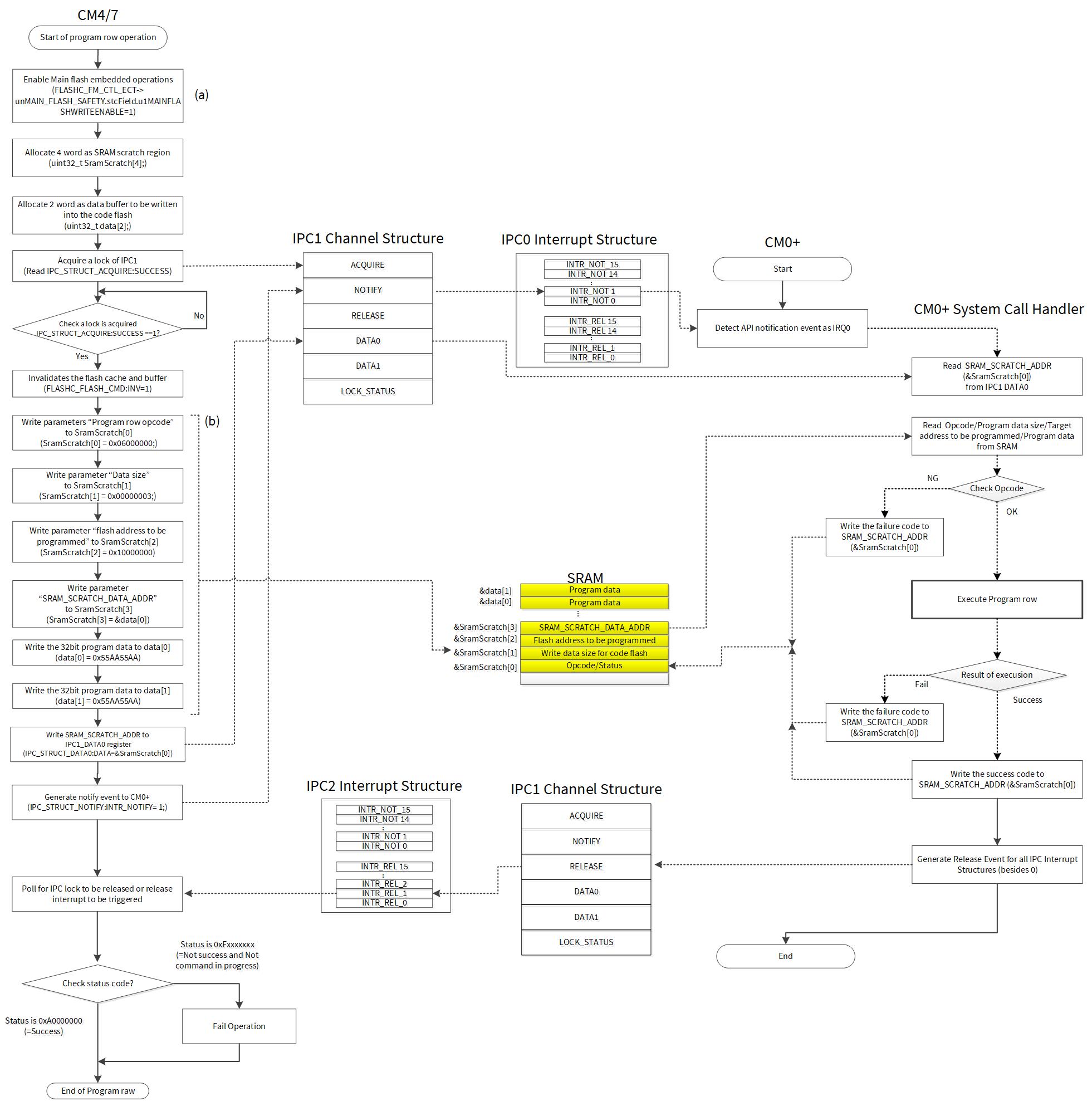
Configuration and example code
Table 5 lists the functions of the configuration part in the SDL for Program Row.
Functions | Description | Remarks |
|---|---|---|
| Initializes the flash IP | See Code Listing 5 |
| Enables writing the main flash | See Code Listing 2 |
| Enables writing the work flash | See Code Listing 6 |
| Programs data to the address in the code flash | See Code Listing 7 |
| Writes an array of data to a single row of flash | See Code Listing 8 |
Code Listing 4 demonstrates an example program of the Program Row operation.
Code Listing 4 Example of Program Row operation
    int main(void)
    {
    :
        // Initialization
        Cy_FlashInit(false /*blocking*/);  /* Initialize flash IP. See [Code Listing 5](grn1680597195267#cgv1681800130152__example_grq_yjl_2xb). */
    :
        /** Programming **/
        for(uint32_t i_addr = SectorAddr; i_addr < SectorAddr + SectorSizeInByte; i_addr+=SIZE_4096_BIT_IN_BYTE)
        {
            // Flash
            Cy_FlashWriteCode(i_addr, (uint32_t*)programData, CY_FLASH_PROGRAMROW_DATA_SIZE_4096BIT,CY_FLASH_DRIVER_BLOCKING);  /* Program data to address in code flash. See [Code Listing 7](grn1680597195267#cgv1681800130152__example_cx5_dkl_2xb). */
        }

    }
Code Listing 5 Cy_ FlashInit() function
    void Cy_FlashInit(bool non_blocking)
    {
        if(non_blocking == true)
        {
            /******  Setting for IPCs    ******/
            Cy_Srom_SetResponseHandler(Cy_FlashHandler, CPUIntIdx3_IRQn);
            NVIC_SetPriority(CPUIntIdx3_IRQn, 3ul);
            NVIC_EnableIRQ(CPUIntIdx3_IRQn);
            g_NB_ModeEnabled = true;
        }
        else
        {
            g_NB_ModeEnabled = false;
        }

        /*  Flash Write Enable   */
        Cy_Flashc_MainWriteEnable();  /* Enable writing main flash.  See [Code Listing 2](grn1680597195267#eme1681800122059__example_wlk_b3l_2xb). See (a) of [Figure 6](grn1680597195267#cpe1681800128611___Toc48123592). */
        Cy_Flashc_WorkWriteEnable();

        g_completeFlag = true;
    }
<<<<<<< HEAD:docs/grn1680597195267_2.md
=======

>>>>>>> dev:docs/grn1680597195267.mdx
Code Listing 6 Cy_Flashc_WorkWriteEnable() function
    __STATIC_INLINE void Cy_Flashc_WorkWriteEnable(void)
    {
        FLASHC_FM_CTL_ECT->unWORK_FLASH_SAFETY.stcField.u1WORKFLASHWRITEENABLE = 1ul;  /* Enable writing work flash. */
    }
Code Listing 7 Cy_ FlashWriteCode() function
    void Cy_FlashWriteCode(uint32_t writeAddr, const uint32_t* data, cy_en_flash_programrow_datasize_t size, cy_en_flash_driver_blocking_t blocking)
    {
        CY_ASSERT(Cy_Flash_MainBoundsCheck(writeAddr) == CY_FLASH_IN_BOUNDS);

        uint32_t status;
        cy_stc_flash_programrow_config_t programRowConfig = {0};

        if(blocking == CY_FLASH_DRIVER_NON_BLOCKING)
        {
            CY_ASSERT(g_NB_ModeEnabled== true);

            /* Only for non-blocking operation */
            g_completeFlag = false;
        }

        // Program code flash
        programRowConfig.blocking = CY_FLASH_PROGRAMROW_BLOCKING;
        programRowConfig.skipBC   = CY_FLASH_PROGRAMROW_SKIP_BLANK_CHECK;
        programRowConfig.dataSize = size;
        programRowConfig.dataLoc  = CY_FLASH_PROGRAMROW_DATA_LOCATION_SRAM;
        programRowConfig.intrMask = CY_FLASH_PROGRAMROW_NOT_SET_INTR_MASK;
        programRowConfig.destAddr = (uint32_t*)writeAddr;
        programRowConfig.dataAddr = data;
        status = Cy_Flash_ProgramRow(NULL, &programRowConfig, blocking);  /* Program addressed flash. See [Code Listing 8](grn1680597195267#cgv1681800130152__example_ipz_hkl_2xb). See (b) of [Figure 6](grn1680597195267#cpe1681800128611___Toc48123592). */

        CY_ASSERT(status == CY_FLASH_DRV_SUCCESS);
    }
Code Listing 8 Cy_Flash_ProgramRow() function
    cy_en_flashdrv_status_t Cy_Flash_ProgramRow(cy_un_flash_context_t* context, const cy_stc_flash_programrow_config_t* config, cy_en_flash_driver_blocking_t block)
    {
        /* Checks if input pointers are not NULL */
        if(config == NULL)
        {
            return CY_FLASH_DRV_INVALID_INPUT_PARAMETERS;
        }

        /* Checks if input address are valid */
        if((Cy_Flash_BoundsCheck((uint32_t)config->destAddr) == CY_FLASH_OUT_OF_BOUNDS) || (config->dataAddr == NULL))
        {
            return CY_FLASH_DRV_INVALID_INPUT_PARAMETERS;
        }

        /* Prepares arguments to be passed to SROM API */
        un_srom_api_args_t apiArgs = { 0ul };
        apiArgs.ProgramRow.arg0.opcode         = CY_SROM_OP_FLASH_PROGRAM_ROW;
        apiArgs.ProgramRow.arg0.blocking       = config->blocking;
        apiArgs.ProgramRow.arg0.skipBlankCheck = config->skipBC;
        apiArgs.ProgramRow.arg1.dataLoc        = config->dataLoc;
        apiArgs.ProgramRow.arg1.dataSize       = config->dataSize;
        apiArgs.ProgramRow.arg1.interruptMask  = config->intrMask;
        apiArgs.ProgramRow.arg2.dstAddr        = (uint32_t)config->destAddr;
        apiArgs.ProgramRow.arg3.srcAddr        = (uint32_t)config->dataAddr;

        /* Call SROM API driver and process response */
        return Cy_Flash_CallSromApiForFlashWrite(&apiArgs, block);
    }
Flash rewriting using dual bank approach
This section shows an example of flash rewriting using flash dual bank approach to enable the over-the-air (OTA) firmware update functionality.
Concept
In TRAVEO™ T2G family MCUs, the OTA functionality is handled by two separate registers. The Flash Main Bank Mode register is to configure the flash bank mode between “Single” and “Dual banks”. The Flash Main Remap register is to configure the flash region between “Mapping A and B”. Both Flash Main Bank Mode and Flash Main Remap registers are cleared by reset. ROM and flash boot will not touch these configurations. In other words, TRAVEO™ T2G family MCU always boots up in single bank mode before CM0+ program starts; then you need to configure dual bank and remap function in your respective program.
In this example, the remap parameter is stored in the work flash; the CM0+ program configures the remap after reading from the work flash. Unintended bank switching may cause a serious system failure. It is recommended to implement an appropriate protection mechanism for the system such as duplicating of switching the data or adding check code to prevent unintended bank switching. For safeguarding the remap parameter that is stored in the work flash, memory protection units (MPU) and shared memory protection units (SMPU) provide the memory protection for the work flash. For more details, see the “Protection Unit” chapter in the architecture TRM.
Starting the first application
This section explains how the flash memory and related functions perform while starting the first application. Figure 7 shows entire process.
- After reset, CM4/7 and CM0+ start ROM boot. CM4/7 loops by wait for interrupt (WFI) in ROM boot until activation by CM0+.
- After the completion of ROM boot and flash boot, CM0+ executes its user program code in the code flash.
- The CM0+ user program code configures the flash main bank mode to dual bank mode. Flash mapping is split into two halves, and each half is presented as a separate address region.
- The CM0+ user program code checks the remap parameter from certain known work flash area. If the data read from the work flash is as expected, the CM0+ user program changes the remap control. At the initial state, when no firmware update request is received, no remap control is being executed because the remap parameter will be pointing to the original code.
- The CM0+ user program sets the program counter of CM4/7 user program, and then the CM4/7 user program in Bank 0 starts.
Figure 7. Starting the first application 
Flash reprogramming
This section explains the firmware update using flash dual bank modes. Figure 8 shows the entire process.
- The CM4/7 user program code in Bank 0 receives the firmware update request and data via vehicle LAN such as CAN FD or Ethernet.
- The CM0+ user program starts erasing the entire area of code flash Bank 1 and certain work flash area, which contains the remap parameter.
- After the completion of flash erasing, the CM0+ user program copies the same CM0+ user program code to code flash Bank 1 and programs the new user program code for CM4/7.
- Finally, CM0+ updates the remap parameter in the work flash, which is used to perform switching of the application code at the next reset. The remap parameter would be any key code or start address of the user program code and so on depending on the application use case.
Note: In case of enabling cache on CYT4B series, you should set the MPU as non-cacheable for the following memory.
-
SRAM scratch area which is used by IPC
-
Work flash area
Figure 8. Flash reprogramming 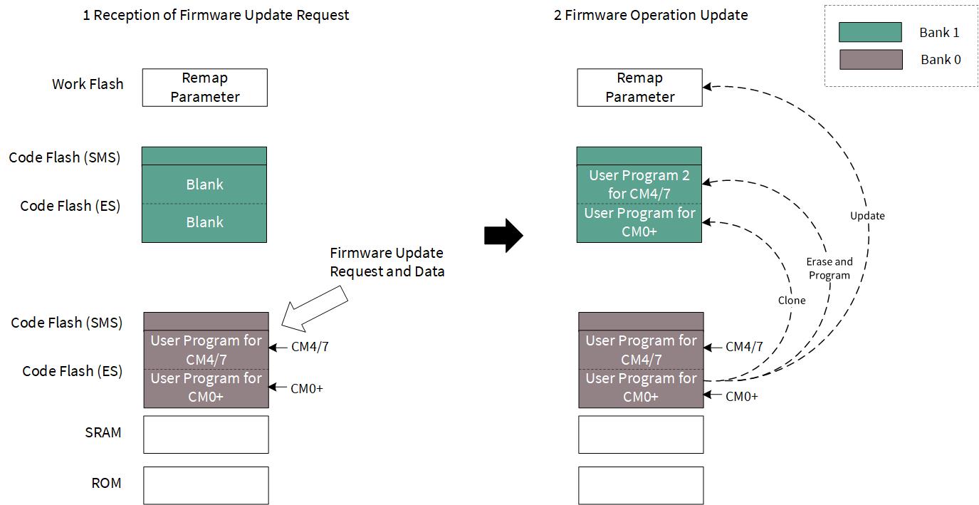
Starting new CM4/7 user program code
This section explains the example how a new CM4/7 user program code starts after switching the code flash bank. Figure 9 shows entire process.
- Once the new user code is programmed and the remap parameter is updated, the user code resets the MCU. After the reset, CM4/7 and CM0+ execute the boot code in ROM.
- The CM0+ user program configures the flash main bank mode to dual bank mode. Flash mapping is split into two halves, and each half is presented as a separate address region. After that, the CM0+ user program reads the remap parameter from the work flash.
- If the data read from work flash is an expected value, CM0+ jumps to the SRAM code, and then changes the flash region to “Mapping B” by setting the Flash Main Remap register.
- After the completion of switching operation, address of code flash bank 0 will be swapped with code flash bank 1. CM4/7 and CM0+ can read the flash memory of bank 1 by using the same address.
- CM0+ jumps back to the flash code. Now, the same CM0+ user program should be there. CM0+ sets the program counter of CM4/7 to the new user program code, from where its execution is started.
Figure 9. Starting new CM4/7 user program code 
Flash rewriting procedure using dual bank mode and remap function
This section shows the example of the flash rewriting procedure using dual bank mode and the remap function. In this example, the user LED ON/OFF program is updated by the firmware update request. The Work flash SA0 sector is used for storing the remap parameters; then the CM0+ code reads the data from the work flash and configures the mapping. If the data read from the work flash is “0xAAAA_AAAA”, mapping A is performed. If the data read is “0xBBBB_BBBB”, mapping B is performed. The user application code is swapped; it depends on the remap parameter in the work flash.
Figure 10. Procedure to start new CM4/7 user program code 
Configuration and example code
Table 6 lists the parameters and Table 7 lists the functions of the configuration part in the SDL for flash rewriting procedure.
Parameters | Description | Value |
|---|---|---|
| Flash remap parameter | 0 |
| Flash memory flag | 1 |
| Firmware update request | 0 |
Functions | Description | Remarks |
|---|---|---|
| Enables writing the main flash | See Code Listing 2 |
| Enables writing the work flash | See Code Listing 6 |
| Sets the bank mode for the main flash | See Code Listing 10 |
| Disables the flash cache | See Code Listing 11 |
| Invalidates the flash cache and buffer | See Code Listing 12 |
| Erases work flash sector SA0 | See Code Listing 13 |
| Erases code flash logical bank | See Code Listing 14 |
| Copies the code flash to Bank 1 | See Code Listing 15 |
| Programs data B | See Code Listing 16 |
| Copies the code flash to Bank 0 | See Code Listing 17 |
| Programs data A | See Code Listing 18 |
Code Listing 9 demonstrates an example program of flash rewriting procedure.
Code Listing 9 Example of flash rewriting procedure
    uint32_t flash_remap_config = 0;
    bool Memory_result = 1;

    int main(void)
    {
    :
        /* Set Write Enable for Code/Work Flash */  /* Enable writing main flash. See [Code Listing 2](grn1680597195267#eme1681800122059__example_wlk_b3l_2xb). Enable writing work flash. See [Code Listing 6](grn1680597195267#cgv1681800130152__example_wd1_bkl_2xb). See (a) of [Figure 10](grn1680597195267#mnf1681800139154___Hlk90298712). */

        Cy_Flashc_MainWriteEnable();
        Cy_Flashc_WorkWriteEnable();

        /* Set Code Flash Bank Mode to "Dual Bank Mode" */  /* Sets Dual bank mode. See [Code Listing 10](grn1680597195267#ngl1681800140478__example_n1w_2rl_2xb). See (b) of [Figure 10](grn1680597195267#mnf1681800139154___Hlk90298712). */
        Cy_Flashc_SetMainBankMode(CY_FLASH_DUAL_BANK_MODE);

        /* Disable CM0+ Flash Cache. */  /* Disables Flash cache. See [Code Listing 11](grn1680597195267#ngl1681800140478__example_yyy_3ql_2xb). See (c) of [Figure 10](grn1680597195267#mnf1681800139154___Hlk90298712). */
        Cy_Flashc_CM0_CacheDisable();
        /* Invalidate Flash Cache Buffer */
        Cy_Flashc_InvalidateFlashCacheBuffer();  /* Invalidates the flash cache and buffer. See [Code Listing 12](grn1680597195267#ngl1681800140478__example_yc2_lql_2xb). See (d) of [Figure 10](grn1680597195267#mnf1681800139154___Hlk90298712). */


        /* Read value from 0x14000000 */
        flash_remap_config = *(volatile unsigned long *)0x14000000;

        if(flash_remap_config != 0xAAAAAAAA && flash_remap_config  != 0xBBBBBBBB)
        {
            Memory_result = 0;
            /* clear */
            EraseSectorWorkSectors_SA0();  /* If WorkFlash SA0 is neither 0xAAAAAAAA nor 0xBBBBBBBB, erase WorkFlash SA0. See [Code Listing 13](grn1680597195267#ngl1681800140478__example_arw_nql_2xb). */
        }

        /* Read Remap parameter from WorkFlash SA0 and Change Remap Operation */
        if(flash_remap_config == 0xAAAAAAAA)
        {
            /* Switch to Map A */
            //SwitchMapA();  /* Read WorkFlash SA0 =0xAAAAAAAA. Switch to Flash Map A. See [Code Listing 10](grn1680597195267#ngl1681800140478__example_n1w_2rl_2xb). See (e) and (f) of [Figure 10](grn1680597195267#mnf1681800139154___Hlk90298712). */
            Cy_Flashc_SetMainBankMode(CY_FLASH_MAPPING_A);
        }
        else if(flash_remap_config == 0xBBBBBBBB)
        {
            /* Switch to Map B */
            //SwitchMapB();    /* Read WorkFlash SA0 =0xAAAAAAAA. Switch to Flash Map A. See [Code Listing 10](grn1680597195267#ngl1681800140478__example_n1w_2rl_2xb). See (g) and (h) of [Figure 10](grn1680597195267#mnf1681800139154___Hlk90298712). */
            Cy_Flashc_SetMainBankMode(CY_FLASH_MAPPING_B);
        }

        /* Enable CM7_0. CY_CORTEX_M7_APPL_ADDR is calculated in linker script, check it in case of problems. */
        Cy_SysEnableApplCore(CORE_CM7_0, CY_CORTEX_M7_0_APPL_ADDR);  /* Active CM7_0. See (i) of [Figure 10](grn1680597195267#mnf1681800139154___Hlk90298712). */


        /* The flag "Update_request" will change to 1 after push button*/
        int Update_request = 0;


        if((Update_request == 1) && (Cy_GPIO_Read(USER_BUTTON_PORT, USER_BUTTON_PIN) == 1/* avoid to button long presses */ ))  /* Update request. See (j) of [Figure 10](grn1680597195267#mnf1681800139154___Hlk90298712). */
        {
            /* Flag clear */
            Update_request = 0;

            if(Memory_result == 0 || flash_remap_config == 0xAAAAAAAA)
            {
                /* MAP A BANK 1: 0x12000000 */

                /* Erase Code Region of Logical Bank 1(0x1200 0000~ 0x12078000) */  /* Read WorkFlash SA0 =0xAAAAAAAA. Erase Code Flash Logical Bank 1. See [Code Listing 14](grn1680597195267#ngl1681800140478__example_z2c_qql_2xb). See (k) and (m) of [Figure 10](grn1680597195267#mnf1681800139154___Hlk90298712). */
                EraseCodeFlashLogicalBank();
                /* Clone CM0+ Code and Program New CM4/7
    User Code to Logical Bank1(0x1200 0000~ 0x121F8000) */  /* Copy to Bank 1. See [Code Listing 15](grn1680597195267#ngl1681800140478__example_sxh_sql_2xb). See (n) of [Figure 10](grn1680597195267#mnf1681800139154___Hlk90298712). */
                CloneCodeFlashtoBank1_UpdateCM7_CODE();
                /* Program Remap Parameter (0xBBBB BBBB) for Work Flash SA0 */
                EraseSectorWorkSectors_SA0();
                ProgramRow_B();  /* Program Data B. See [Code Listing 16](grn1680597195267#ngl1681800140478__example_zkj_lrl_2xb). See (o) of [Figure 10](grn1680597195267#mnf1681800139154___Hlk90298712). */
            }
            else
            {
                if(flash_remap_config  == 0xBBBBBBBB)
                {
                    /* MAP B BANK 0: 0x12000000 */
                    /* Read WorkFlash SA0 =0xBBBBBBBB. Erase Code Flash Logical Bank 0. See  [Code Listing 14](grn1680597195267#ngl1681800140478__example_z2c_qql_2xb), [Code Listing 18](grn1680597195267#ngl1681800140478__example_zw5_4rl_2xb). See (p), (q) of [Figure 10](grn1680597195267#mnf1681800139154___Hlk90298712). */
                    /* Erase Code Region of Logical Bank 0(0x1200 0000~ 0x12078000) */
                    EraseCodeFlashLogicalBank();
                    /* Clone CM0+ Code and Program New CM4/7
    User Code to Logical Bank0(0x1200 0000~ 0x121F8000) */  /* Copy to Bank 0. See [Code Listing 17](grn1680597195267#ngl1681800140478__example_wkn_wql_2xb). See (r) of [Figure 10](grn1680597195267#mnf1681800139154___Hlk90298712). */
                    CloneCodeFlashtoBank0_UpdateCM7_CODE();
                    /* Program Remap Parameter (0xAAAA_AAAA) for Work Flash SA0 */
                    EraseSectorWorkSectors_SA0();
                    ProgramRow_A();  /* Program Data A. See [Code Listing 18](grn1680597195267#ngl1681800140478__example_zw5_4rl_2xb). See (s) of [Figure 10](grn1680597195267#mnf1681800139154___Hlk90298712). */
                }
            }
<<<<<<< HEAD:docs/grn1680597195267_2.md

=======
>>>>>>> dev:docs/grn1680597195267.mdx
Code Listing 10 Cy_Flashc_SetMainBankMode() function
    __STATIC_INLINE void Cy_Flashc_SetMainBankMode(cy_en_bankmode_t mode)  /* Sets bank mode for main flash. */
    {
       FLASHC->unFLASH_CTL.stcField.u1MAIN_BANK_MODE = mode;
       FLASHC->unFLASH_CTL.u32Register;
    }
Code Listing 11 Cy_Flashc_CM0_CacheDisable() function
    __STATIC_INLINE void Cy_Flashc_CM0_CacheDisable(void)  /* Disables Flash cache. */
    {
        FLASHC->unCM0_CA_CTL0.stcField.u1CA_EN = 0ul;
    }
Code Listing 12 Cy_Flashc_InvalidateFlashCacheBuffer() function
    __STATIC_INLINE void Cy_Flashc_InvalidateFlashCacheBuffer(void)  /* Invalidates the flash cache and buffer. */
    {
        FLASHC->unFLASH_CMD.stcField.u1INV = 0x1ul;

        // Wait for completion (HW will clear bit)
        while(FLASHC->unFLASH_CMD.stcField.u1INV != 0);
    }
Code Listing 13 EraseSectorWorkSectors_SA0() function
    void EraseSectorWorkSectors_SA0(void)  /* Erase workflash sector SA0. */
    {
        uint32_t status = CY_FLASH_DRV_SUCCESS;

        /* 1.1. Erase workflash sector SA0    */
        status = Cy_Flash_EraseSector(&FlashContext, &eraseSectorConfigSA0, CY_FLASH_DRIVER_BLOCKING);
        /* 1.2. Status check    */
        CY_ASSERT(status == CY_FLASH_DRV_SUCCESS);
        /* 1.3. Verify    */
        status = Cy_Flash_BlankCheck(&FlashContext, &blankCheckConfig, CY_FLASH_DRIVER_BLOCKING);
        CY_ASSERT(status == CY_FLASH_DRV_SUCCESS);
    }
Code Listing 14 EraseCodeFlashLogicalBank() function
    void EraseCodeFlashLogicalBank(void)  /* Erase Code Flash Logical Bank. */
    {
        uint32_t status = CY_FLASH_DRV_SUCCESS;

        for(uint32_t addrOffset = 0; addrOffset < CODE_FLASH_REGION_SIZE; addrOffset += CODE_FLASH_SECTOR_SIZE)
        {
            // Set the address to be erased.
            // Note: This firmware always erases logical area 0 from (0x1200_0000 ~ ).
            eraseCodeSectorConfig.Addr = (uint32_t*)(CODE_FLASH_LOGICAL_TOP_ADDR1 + addrOffset);
            // Issuing the erase sector
            status = Cy_Flash_EraseSector(&FlashContext, &eraseCodeSectorConfig, CY_FLASH_DRIVER_BLOCKING);
            // Checking the result
            CY_ASSERT(status == CY_FLASH_DRV_SUCCESS);
        }
    }
Code Listing 15 CloneCodeFlashtoBank1_UpdateCM7_CODE() function
    void CloneCodeFlashtoBank1_UpdateCM7_CODE(void)  /* Copy Code Flash to Bank 1. */
    {

        uint32_t status = CY_FLASH_DRV_SUCCESS;

        /* 2.1. Program flash whole sector    */
        for(uint32_t addrOffset = 0; addrOffset < SIZE; addrOffset += BYTE_NUM_OF_4096BIT /*0x1000*/)
        {
            // Copy the Flash contents into temporaly buffer
            memcpy((void*)bufToBeProgramed, (void*)(CODE_FLASH_LOGICAL_TOP_ADDR0/* 0x10000000*/ + addrOffset), BYTE_NUM_OF_4096BIT);

            ProgramRow.destAddr = (uint32_t*)(CODE_FLASH_LOGICAL_TOP_ADDR1 + addrOffset);
            ProgramRow.dataAddr = (uint32_t*)&bufToBeProgramed[addrOffset];

            status = Cy_Flash_ProgramRow(&FlashContext, &ProgramRow, CY_FLASH_DRIVER_BLOCKING);
            CY_ASSERT(status == CY_FLASH_DRV_SUCCESS);
        }

        /* CM7 data upodat */
        for(uint32_t i = 0; i<2 ;i+=1)
        {
            uint32_t ADDR_LED = 0x10080410;
            programRow_LED.destAddr = (uint32_t*)(ADDR_LED + (i<<3));
            programRow_LED.dataAddr = (uint32_t*)&CM7_DATA2[i<<3];
            programRow_LED.dataSize = CY_FLASH_PROGRAMROW_DATA_SIZE_64BIT;
            status = Cy_Flash_ProgramRow(&FlashContext, &programRow_LED, CY_FLASH_DRIVER_BLOCKING);
            CY_ASSERT(status == CY_FLASH_DRV_SUCCESS);
        }

    }
Code Listing 16 ProgramRow_B() function
    void ProgramRow_B(void)
    {
        uint32_t status = CY_FLASH_DRV_SUCCESS;  /* Program Data B. */

        /* 2.1. Program flash whole sector    */
        for(uint32_t offsetAddr = 0; offsetAddr < TEST_ERASE_SEC_SIZE; offsetAddr += TEST_PROGRAM_SIZE)
        {
            programRowConfigSA0.destAddr = (uint32_t*)(TEST_FLASH_ADDR + offsetAddr);
            programRowConfigSA0.dataAddr = writeData_B;
            status = Cy_Flash_ProgramRow(&FlashContext, &programRowConfigSA0, CY_FLASH_DRIVER_BLOCKING);
            CY_ASSERT(status == CY_FLASH_DRV_SUCCESS);
        }
    }
Code Listing 17 CloneCodeFlashtoBank0_UpdateCM7_CODE() function
    void CloneCodeFlashtoBank0_UpdateCM7_CODE(void)  /* Copy Code Flash to Bank 0. */
    {
        uint32_t status = CY_FLASH_DRV_SUCCESS;
        /* 2.1. Program flash whole sector    */
        for(uint32_t addrOffset = 0; addrOffset < SIZE ;addrOffset += BYTE_NUM_OF_4096BIT /*0x1000*/)
        {
            // Copy the Flash contents into temporaly buffer
            memcpy((void*)bufToBeProgramed, (void*)(CODE_FLASH_LOGICAL_TOP_ADDR0 + addrOffset), BYTE_NUM_OF_4096BIT);

            ProgramRow.destAddr = (uint32_t*)(CODE_FLASH_LOGICAL_TOP_ADDR1 + addrOffset);
            ProgramRow.dataAddr = (uint32_t*)&bufToBeProgramed[addrOffset];
            status = Cy_Flash_ProgramRow(&FlashContext, &ProgramRow, CY_FLASH_DRIVER_BLOCKING);
            CY_ASSERT(status == CY_FLASH_DRV_SUCCESS);
        }
        /* CM7 data upodat */
        uint32_t ADDR_LED = 0x10080410;
        for(uint32_t i = 0; i<2 ;i+=1)
        {
            programRow_LED.destAddr = (uint32_t*)(ADDR_LED + (i<<3));
            programRow_LED.dataAddr = (uint32_t*)&CM7_DATA1[i<<3];
            programRow_LED.dataSize = CY_FLASH_PROGRAMROW_DATA_SIZE_64BIT;
            status = Cy_Flash_ProgramRow(&FlashContext, &programRow_LED, CY_FLASH_DRIVER_BLOCKING);
            CY_ASSERT(status == CY_FLASH_DRV_SUCCESS);
        }
    }
Code Listing 18 ProgramRow_A() function
    void ProgramRow_A(void)  /* Program Data A. */
    {
        uint32_t status = CY_FLASH_DRV_SUCCESS;

        /* 2.1. Program flash whole sector    */
        for(uint32_t offsetAddr = 0; offsetAddr < TEST_ERASE_SEC_SIZE; offsetAddr += TEST_PROGRAM_SIZE)
        {
            programRowConfigSA0.destAddr = (uint32_t*)(TEST_FLASH_ADDR + offsetAddr);
            programRowConfigSA0.dataAddr = writeData_A;
            status = Cy_Flash_ProgramRow(&FlashContext, &programRowConfigSA0, CY_FLASH_DRIVER_BLOCKING);
            CY_ASSERT(status == CY_FLASH_DRV_SUCCESS);
        }
        /* 2.2. Veryfy    */
        for(uint32_t offsetAddr = 0; offsetAddr < TEST_ERASE_SEC_SIZE; offsetAddr += 4)
        {
            CY_ASSERT(*(uint32_t*)(TEST_FLASH_ADDR + offsetAddr) == DATA_TO_BE_PROGRAMED_A);
        }
    }
Work flash reading procedure
In TRAVEO™ T2G family, the work flash can be read via different CPU cores, but only one CPU core is assigned for non-correctable ECC error handling. When an ECC error occurs, the CPU core handling the error must inform the other CPU cores about the error. However, this is time consuming. Moreover, in CYT3/CYT4/CYT6 series, reading of the work flash via AXI bus (64-bit) always checks for ECC errors in all 64 bits, even if 8-, 16-, or 32-bit load instructions are used. This can lead to ECC errors even if the addressed memory does not have an ECC error. Therefore, it is recommended to use AHB (32-bit) DMA (M-DMA or P-DMA) channels to read the work flash. Each CPU core should be assigned a DMA channel. The DMA channel can detect any non-correctable errors, including ECC double-bit errors. DMA reports the bus error for the individual channel that encountered faulty access; error detection is accurate by units of 32 bits.
If an application needs to distinguish between an ECC error and other errors, handle the fault structure with one CPU core only. The same fault cannot be reliably routed to fault structures of multiple cores.
This section shows an example of the work flash reading procedure using AHB DMA (M-DMA or P-DMA) channels.
Work flash reading procedure via DMA
Figure 11 shows an example of the work flash reading procedure via DMA.
Figure 11. Work flash reading procedure via DMA 
- Disable the DMA channel configuration.
- Configure the DMA channel such as the channel priority and pointer address of the descriptor corresponding to the configured channel.
- Configure the DMA descriptor such as descriptor type, source address (work flash address), destination address (for example, SRAM address), transfer size, data size, and trigger.
- Enable the DMA channel and DMA after configuring the DMA channel.
- Configure the fault report structure such as the fault source (work flash non-correctable ECC error) and fault action (only capture the fault information; do not use interrupt).
- Trigger the DMA channel. For example, use the software trigger via the trigger multiplexer.
- CPU reads the data from the destination address after the DMA transfer completed.
If a non-correctable ECC error occurred in the work flash, each CPU will be able to detect it as a bus error using DMA. The CPU core handling the fault structure can get the fault information from the fault structure.
For details on the DMA and fault configuration procedure, see AN219842, AN220191, and registers TRM listed in #dxv1681800147971.
Configuration and example code
Table 8 lists the configuration parameters and Table 9 the functions of the configuration part in the SDL for the work flash reading procedure via DMA.
Parameters | Description | Value |
|---|---|---|
| Defines the buffer size | 36 |
| Defines the M-DMA channel | 0 |
| Defines the SW trigger | TRIG_OUT_MUX_3_MDMA_TR_IN0 |
| M-DMA current descriptor pointer | &stcDescr |
| Channel preemptable | 0ul |
| Channel priority | 0ul |
| Channel enable | 1ul |
| DESCR_CTL WAIT_FOR_DEACT | 0ul |
| DESCR_CTL INTR_TYPE | CY_MDMA_INTR_DESCR_CMPLT |
| DESCR_CTL TR_OUT_TYPE | CY_MDMA_TRIGOUT_DESCR_CMPLT |
| DESCR_CTL DATA_PREFETCH | 0ul |
| DESCR_CTL CH_DISABLE | CY_MDMA_CH_DISABLED |
| DESCR_CTL TR_IN_TYPE | CY_MDMA_TRIGIN_DESCR |
| DESCR_CTL DATA_SIZE | CY_MDMA_BYTE |
| DESCR_CTL SRC_TRANSFER_SIZE | 0ul |
| DESCR_CTL DST_TRANSFER_SIZE | 0ul |
| DESCR_TYPE | CY_MDMA_MEMORY_COPY_TRANSFER |
| DESCR_SRC | au8SrcBuffer |
| DESCR_DST | au8DestBuffer |
| DESCR_X_CTL X_COUNT | BUFFER_SIZE |
| DESCR_NEXT_PTR | NULL |
Functions | Description | Remarks |
|---|---|---|
| Configures M-DMA disable | See Code Listing 20 |
| Clears all the content of registers corresponding to the channel | See Code Listing 21 |
| Configures M-DMA channel initialize | See Code Listing 22 |
| Configures M-DMA descriptor initialize | See Code Listing 23 |
| Configures M-DMA channel enable | See Code Listing 24 |
| Configures M-DMA enable | See Code Listing 25 |
| Generates a software trigger | See Code Listing 26 |
Code Listing 19 demonstrates an example program of the flash rewriting procedure.
Code Listing 19 Example of work flash reading procedure via DMA
    #define BUFFER_SIZE     (36ul)  /* Defines buffer size. */
    #define DMAC_CHANNEL    (0)  /* Defines M-DMA. */
    #define DMAC_SW_TRIG    (TRIG_OUT_MUX_3_MDMA_TR_IN0)   /* Defines SW trigger */
    /* Configure M-DMA channel. */
    static const   cy_stc_mdma_chnl_config_t   chnlConfig =
    {
        .MDMA_Descriptor = &stcDescr,
        .preemptable     = 0ul,
        .priority        = 0ul,
        .enable          = 1ul,         /* enabled after initialization */
    };
    static const cy_stc_mdma_descr_config_t  stcDmaDescrConfig =  /* Configure M-DMA descriptor. */
    {
        .deact          = 0ul,
        .intrType       = CY_MDMA_INTR_DESCR_CMPLT,
        .trigoutType    = CY_MDMA_TRIGOUT_DESCR_CMPLT,
        .dataPrefetch   = 0ul,
        .chStateAtCmplt = CY_MDMA_CH_DISABLED,
        .triginType     = CY_MDMA_TRIGIN_DESCR,
        .dataSize       = CY_MDMA_BYTE,
        .srcTxfrSize    = 0ul,
        .destTxfrSize   = 0ul,
        .descrType      = CY_MDMA_MEMORY_COPY_TRANSFER,
        .srcAddr        = au8SrcBuffer,
        .destAddr       = au8DestBuffer,
        .xCount         = BUFFER_SIZE,
        .descrNext      = NULL
    };

    int main(void)
    {
    :
        /* Disable DMA CH0  */  /* Disable M-DMA. See [Code Listing 20](grn1680597195267#drl1681800145195__example_e2q_d3s_2xb). See (a) of [Figure 11](grn1680597195267#xsd1681800143365___Ref90298780). Clears all the content of registers corresponding to the channel. See [Code Listing 21](grn1680597195267#drl1681800145195__example_m3g_g3s_2xb). */
        Cy_MDMA_Disable(DMAC);
        Cy_MDMA_Chnl_DeInit(DMAC, DMAC_CHANNEL);
        /* Configure DMA CH0 */  /* Configures M-DMA channel initialize. See [Code Listing 22](grn1680597195267#drl1681800145195__example_xtb_j3s_2xb). See (b) of [Figure 11](grn1680597195267#xsd1681800143365___Ref90298780). */
        Cy_MDMA_Chnl_Init(DMAC, DMAC_CHANNEL, &chnlConfig);
        /* Configure DMA Descriptor */  /* Configures M-DMA descriptor initialize. See [Code Listing 23](grn1680597195267#drl1681800145195__example_zfd_l3s_2xb). See (c) of [Figure 11](grn1680597195267#xsd1681800143365___Ref90298780). */
        Cy_MDMA_Descr_Init(&stcDescr,&stcDmaDescrConfig);
        /* Enable DMA channel 0 and DMA */  /*Configures M-DMA channel enable. See [Code Listing 24](grn1680597195267#drl1681800145195__example_gwj_n3s_2xb). Configures M-DMA enable. See [Code Listing 25](grn1680597195267#drl1681800145195__example_blp_p3s_2xb). See (d) of [Figure 11](grn1680597195267#xsd1681800143365___Ref90298780). */
        Cy_MDMA_Chnl_Enable(DMAC, DMAC_CHANNEL);
        Cy_MDMA_Enable(DMAC);

        /* SW Trigger */  /* Generates a Software trigger. See [Code Listing 26](grn1680597195267#drl1681800145195__example_xkd_s3s_2xb). See (e) of [Figure 11](grn1680597195267#xsd1681800143365___Ref90298780). */
        Cy_TrigMux_SwTrigger(DMAC_SW_TRIG, TRIGGER_TYPE_EDGE, 1ul);

        /* Read DATA from destination after DMA transfer completed.*/
        for(uint32_t i = 0ul; i < BUFFER_SIZE; i++)
        {
            READ_DATA[i] = au8DestBuffer[i];  /* CPU read Data. See (f) of [Figure 11](grn1680597195267#xsd1681800143365___Ref90298780). */
        }

        /* Fault status read  */
        status = Cy_SysFlt_GetErrorSource(FAULT_STRUCT0);

        for(;;);
    }
Code Listing 20 Cy_MDMA_Disable() function
    void Cy_MDMA_Disable(volatile stc_DMAC_t *pstcMDMA)  /* Write to M-DMA_CTL_ENABLED bit */
    {
        pstcMDMA->unCTL.stcField.u1ENABLED  =       0ul;
    }
Code Listing 21 Cy_MDMA_Chnl_DeInit() function
    void Cy_MDMA_Chnl_DeInit(volatile stc_DMAC_t *pstcMDMA, uint32_t chNum)  /* Clears all the content of registers corresponding to the channel bit */
    {
        pstcMDMA->CH[chNum].unCTL.u32Register               = 0ul;
        pstcMDMA->CH[chNum].unIDX.u32Register               = 0ul;
        pstcMDMA->CH[chNum].unCURR.u32Register              = 0ul;
        pstcMDMA->CH[chNum].unINTR_MASK.u32Register         = 0ul;
        pstcMDMA->CH[chNum].unINTR_SET.u32Register          = 0ul;
    }
Code Listing 22 Cy_MDMA_Chnl_Init() function
    cy_en_mdma_status_t Cy_MDMA_Chnl_Init(volatile stc_DMAC_t *pstcMDMA, uint32_t chNum, const cy_stc_mdma_chnl_config_t* chnlConfig)  /* Configures M-DMA channel initialize */
    {
        cy_en_mdma_status_t retVal = CY_MDMA_ERR_UNC;

        if ((pstcMDMA != NULL) && (chnlConfig != NULL))
        {
            /* Set current descriptor */
            pstcMDMA->CH[chNum].unCURR.u32Register   =  (uint32_t)chnlConfig->MDMA_Descriptor;

            /* Set if the channel is preemptable  */
            /* There is no the parameter in MDMA */

            /* Set channel priority */
            pstcMDMA->CH[chNum].unCTL.stcField.u2PRIO    =   chnlConfig->priority;

            /* Set enabled status */
            pstcMDMA->CH[chNum].unCTL.stcField.u1ENABLED =   chnlConfig->enable;

            retVal = CY_MDMA_SUCCESS;
        }
        else
        {
            retVal = CY_MDMA_INVALID_INPUT_PARAMETERS;
        }

        return (retVal);
    }
Code Listing 23 Cy_MDMA_Descr_Init() function
    cy_en_mdma_status_t Cy_MDMA_Descr_Init(cy_stc_mdma_descr_t* descriptor, const cy_stc_mdma_descr_config_t* config)  /* Configures M-DMA descriptor */
    {
        cy_en_mdma_status_t retVal = CY_MDMA_ERR_UNC;

        if ((descriptor != NULL) && (config != NULL))
        {
            /* Descriptor[0] */
            descriptor->unMDMA_DESCR_CTL.stcField.u2WAIT_FOR_DEACT     =       config->deact;
            descriptor->unMDMA_DESCR_CTL.stcField.u2INTR_TYPE          =       config->intrType;
            descriptor->unMDMA_DESCR_CTL.stcField.u2TR_OUT_TYPE        =       config->trigoutType;
            descriptor->unMDMA_DESCR_CTL.stcField.u2TR_IN_TYPE         =       config->triginType;
            descriptor->unMDMA_DESCR_CTL.stcField.u1DATA_PREFETCH      =       config->dataPrefetch;
            descriptor->unMDMA_DESCR_CTL.stcField.u2DATA_SIZE          =       config->dataSize;
            descriptor->unMDMA_DESCR_CTL.stcField.u1CH_DISABLE         =       config->chStateAtCmplt;
            descriptor->unMDMA_DESCR_CTL.stcField.u1SRC_TRANSFER_SIZE  =       config->srcTxfrSize;
            descriptor->unMDMA_DESCR_CTL.stcField.u1DST_TRANSFER_SIZE  =       config->destTxfrSize;
            descriptor->unMDMA_DESCR_CTL.stcField.u3DESCR_TYPE         =       config->descrType;

            /* Descriptor[1] */
            descriptor->u32MDMA_DESCR_SRC                              =       (uint32_t)config->srcAddr;

            /* after 3rd word of descriptor depends on descriptor type */

            switch(config->descrType)
            {
            case (uint32_t)CY_MDMA_SINGLE_TRANSFER:
            {
                /* Descriptor[2] */
                descriptor->u32MDMA_DESCR_DST                           =       (uint32_t)config->destAddr;

                /* Descriptor[3] -> NEXT_PTR */
                descriptor->unMDMA_DESCR_X_SIZE.u32Register             =       (uint32_t)config->descrNext;
                break;
            }
            case (uint32_t)CY_MDMA_1D_TRANSFER:
            {
                /* Descriptor[2] */
                descriptor->u32MDMA_DESCR_DST                           =       (uint32_t)config->destAddr;

                /* Descriptor[3] */
                descriptor->unMDMA_DESCR_X_SIZE.stcField.u16X_COUNT     =       (uint32_t)((config->xCount) - 1ul);

                /* Descriptor[4] */
                descriptor->unMDMA_DESCR_X_INCR.stcField.u16SRC_X_INCR  =       (uint32_t)config->srcXincr;
                descriptor->unMDMA_DESCR_X_INCR.stcField.u16DST_X_INCR  =       (uint32_t)config->destXincr;

                /* Descriptor[5] -> NEXT_PTR */
                descriptor->unMDMA_DESCR_Y_SIZE.u32Register             =       (uint32_t)config->descrNext;
                break;
            }
            case (uint32_t)CY_MDMA_2D_TRANSFER:
            {
                /* Descriptor[2] */
                descriptor->u32MDMA_DESCR_DST                           =       (uint32_t)config->destAddr;

                /* Descriptor[3] */
                descriptor->unMDMA_DESCR_X_SIZE.stcField.u16X_COUNT     =       (uint32_t)((config->xCount) - 1ul);

                /* Descriptor[4] */
                descriptor->unMDMA_DESCR_X_INCR.stcField.u16SRC_X_INCR  =       (uint32_t)config->srcXincr;
                descriptor->unMDMA_DESCR_X_INCR.stcField.u16DST_X_INCR  =       (uint32_t)config->destXincr;

                /* Descriptor[5] */
                descriptor->unMDMA_DESCR_Y_SIZE.stcField.u16Y_COUNT     =       (uint32_t)((config->yCount) - 1ul);

                /* Descriptor[6] */
                descriptor->unMDMA_DESCR_Y_INCR.stcField.u16SRC_Y_INCR  =       (uint32_t)config->srcYincr;
                descriptor->unMDMA_DESCR_Y_INCR.stcField.u16DST_Y_INCR  =       (uint32_t)config->destYincr;

                /* Descriptor[7] */
                descriptor->u32MDMA_DESCR_NEXT_PTR                      =       (uint32_t)config->descrNext;
                break;
            }
            case (uint32_t)CY_MDMA_MEMORY_COPY_TRANSFER:
            {
                /* Descriptor[2] */
                descriptor->u32MDMA_DESCR_DST                           =       (uint32_t)config->destAddr;

                /* Descriptor[3] */
                descriptor->unMDMA_DESCR_X_SIZE.stcField.u16X_COUNT     =       (uint32_t)((config->xCount) - 1ul);

                /* Descriptor[4] -> NEXT_PTR */
                descriptor->unMDMA_DESCR_X_INCR.u32Register             =       (uint32_t)config->descrNext;
                break;
            }
            case (uint32_t)CY_MDMA_SCATTER_TRANSFER:
            {
                /* Descriptor[2] -> X_SIZE */
                descriptor->u32MDMA_DESCR_DST                           =       (uint32_t)((config->xCount) - 1ul);

                /* Descriptor[3] -> NEXT_PTR */
                descriptor->unMDMA_DESCR_X_SIZE.u32Register             =       (uint32_t)config->descrNext;
                break;
            }
            default:
            {
                /* Unsupported type of descriptor */
                break;
            }
            }

            retVal = CY_MDMA_SUCCESS;
        }
        else
        {
            retVal = CY_MDMA_INVALID_INPUT_PARAMETERS;
        }

        return retVal;
    }
Code Listing 24 Cy_MDMA_Chnl_ Enable() function
    __STATIC_INLINE void Cy_MDMA_Chnl_Enable(volatile stc_DMAC_t *pstcMDMA, uint32_t chNum)  /* Configures M-DMA channel enable. */
    {
        pstcMDMA->CH[chNum].unCTL.stcField.u1ENABLED = 1ul;
    }
Code Listing 25 Cy_MDMA_ Enable() function
    void Cy_MDMA_Enable(volatile stc_DMAC_t *pstcMDMA)  /* Write to M-DMA_CTL_ENABLED bit */
    {
        pstcMDMA->unCTL.stcField.u1ENABLED  =       1ul;
    }
Code Listing 26 Cy_TrigMux_SwTrigger() function
    cy_en_trigmux_status_t Cy_TrigMux_SwTrigger(uint32_t trigLine, en_trig_type_t trigType, uint32_t outSel)  /* Generates a Software trigger */
    {
        cy_en_trigmux_status_t retVal = CY_TRIGMUX_INVALID_STATE;

        if (PERI->unTR_CMD.stcField.u1ACTIVATE == 0)
        {
            PERI->unTR_CMD.stcField.u8TR_SEL     = Cy_TrigMux_GetNo(trigLine);
            PERI->unTR_CMD.stcField.u5GROUP_SEL  = Cy_TrigMux_GetGroup(trigLine);
            PERI->unTR_CMD.stcField.u1TR_EDGE    = trigType;
            PERI->unTR_CMD.stcField.u1OUT_SEL    = outSel;
            PERI->unTR_CMD.stcField.u1ACTIVATE   = 1;

            retVal = CY_TRIGMUX_SUCCESS;
        }
        return retVal;
    }
Terms and abbreviations
AHB | Advanced high-performance bus |
AXI | Advanced extensible interface |
eCT | Embedded charge-trap |
ECC | Error correcting code |
OTA | Over-the-air |
RAM | Random access memory |
SRAM | Static random-access memory |
P-DMA | Peripheral DMA |
M-DMA | Memory DMA |
IPC | Inter-processer communication |
IRQ | Interrupt request |
DAP | Debug access port |
RWW | Read-while-write |
Related documents
- Device datasheet
- CYT2B7 datasheet 32-bit Arm® Cortex®-M4F microcontroller TRAVEO™ T2G family
- CYT2B9 datasheet 32-bit Arm® Cortex®-M4F microcontroller TRAVEO™ T2G family
- CYT4BF datasheet 32-bit Arm® Cortex®-M7 microcontroller TRAVEO™ T2G family
- CYT4DN datasheet 32-bit Arm® Cortex®-M7 microcontroller TRAVEO™ T2G family (Doc No. 002-24601)
- CYT3BB/4BB datasheet 32-bit Arm® Cortex®-M7 microcontroller TRAVEO™ T2G family
- CYT3DL datasheet 32-bit Arm® Cortex®-M7 microcontroller TRAVEO™ T2G family (Doc No. 002-27763)
- CYT4EN datasheet 32-bit Arm® Cortex®-M7 microcontroller TRAVEO™ T2G family (Doc No. 002-30842)
- CYT2CL datasheet 32-bit Arm® Cortex®-M4F microcontroller TRAVEO™ T2G family (Doc No. 002- 32508)
- CYT6BJ datasheet 32-bit Arm® Cortex®-M7 microcontroller TRAVEO™ T2G family (Doc No. 002-33466)
- Body controller entry family
- TRAVEO™ T2G automotive body controller entry family architecture technical reference manual (TRM)
- TRAVEO™ T2G automotive body controller entry registers technical reference manual (TRM) for CYT2B7
- TRAVEO™ T2G automotive body controller entry registers technical reference manual (TRM) for CYT2B9
- Body controller high family
- TRAVEO™ T2G automotive body controller high family architecture technical reference manual (TRM)
- TRAVEO™ T2G automotive body controller high registers technical reference manual (TRM) for CYT4BF
- TRAVEO™ T2G automotive body controller high registers technical reference manual (TRM) for CYT3BB/4BB
- TRAVEO™ T2G automotive body controller high registers technical reference manual (TRM) for CYT6BJ (Doc No. 002-36068)
- Cluster 2D family
- TRAVEO™ T2G automotive cluster 2D family architecture technical reference manual (TRM) (Doc No. 002-25800)
- TRAVEO™ T2G automotive cluster 2D registers technical reference manual (TRM) for CYT4DN (Doc No. 002-25923)
- TRAVEO™ T2G automotive cluster 2D registers technical reference manual (TRM) for CYT3DL (Doc No. 002-29854)
- Application notes
- AN219842 – How to use interrupt in TRAVEO™ T2G
- AN220191 – How to use direct memory access (DMA) controller in TRAVEO™ T2G family
Other references
A sample driver library (SDL) including startup as sample software to access various peripherals is provided. SDL also serves as a reference to customers for drivers that are not covered by the official AUTOSAR products. The SDL cannot be used for production purposes because it does not qualify to automotive standards. The code snippets in this application note are part of the SDL. Contact Technical support to obtain the SDL.
Revision history
Document version | Date of release | Description of changes |
|---|---|---|
** | 2018-03-09 | New Application Note. |
*A | 2019-06-26 | Changed target parts number (CYT2B/CYT4B series) Added Flash Rewriting Procedure using Dual Bank and Remap Function |
*B | 2020-03-04 | Added a part number CYT2/CYT3/CYT4 series. |
*C | 2020-09-21 | Moved to Infineon Template Changed the document title. Added Work Flash Reading Procedure. Added Application Notes to Related Documents. |
*D | 2021-12-28 | Added example of SDL code and description in all instances. |
*E | 2023-11-10 | Template update; no content update |
*F | 2024-02-09 | Added specifications for CYT6BJ |
© 2024 Infineon Technologies AGOpenDocsPlease read the sections "Important notice" and "Warnings" at the end of this document