AN220222 Low-power mode procedure in TRAVEO™ T2G family
About this document
Scope and purpose
This application note describes the features of low-power modes in TRAVEO™ T2G family MCUs and explains how to enter low-power modes and return to active mode.
Intended audience
This document is intended for anyone who uses the Infineon TRAVEO™ T2G MCUs for using low-power mode.
Associated part family
TRAVEO™ T2G family CYT2/CYT3/CYT4/CYT6 series.
Introduction
This application note describes low-power modes in TRAVEO™ T2G family MCU. The series includes Arm® Cortex® CPUs, CAN FD, memory, and analog and digital peripheral functions in a single chip.
The CYT2 series has one Arm® Cortex®-M4F-based CPU (CM4) and Cortex®-M0+-based CPU (CM0+). The CYT4 series has two Arm® Cortex®-M7-based CPUs (CM7) and CM0+, and the CYT3 series has one CM7 and CM0+. The CYT6 series has four Arm® Cortex®-M7-based CPUs (CM7) and CM0+.
TRAVEO™ T2G family MCUs have several different power modes. These modes are intended to minimize the average power consumption in an application.
This application note explains the features of power modes and how to set up the power mode transition.
To understand the described functionality and terminology used in this application note, see the “Device power modes” chapter of the architecture reference manual .
Power modes of TRAVEO™ T2G family
TRAVEO™ T2G family MCUs have the following power modes:
Active mode: All peripherals are available.
Sleep mode: All peripherals except the CPU are available.
DeepSleep mode: Only low-frequency peripherals are available.
Hibernate mode: Device and I/O states are frozen.
Figure 1 shows the relationship between power modes and the power supply current.
Figure 1.
Power modes and power supply current
Note:
Power consumption is reduced in the order of Active, Sleep, DeepSleep, and Hibernate modes. Each power mode optimizes power consumption for user applications.
Table 1 summarizes the states of each power mode and the entry and wakeup conditions. For more details on power modes, see the architecture reference manual .
Power mode | Description | Entry condition | Wakeup source | Wakeup action |
|---|---|---|---|---|
Active | Primary mode of operation; all peripherals are available (programmable). | Wake up from Sleep/DeepSleep modes, Hibernate reset, or any other reset. | Not applicable | Not applicable |
Sleep | CPU is in Sleep mode; all other peripherals are available. | Interrupt | ||
DeepSleep | All high-frequency clocks and peripherals are turned off. Low-frequency clock (32 kHz) and low-power analog and digital peripherals are available for operation and as wakeup sources. SRAM can be retained (configurable). | Register write from Active modes or debugger session ends. | GPIO interrupt, event generators, SCB, watchdog timer, and RTC alarms 1 and debugger | Interrupt or debug |
Hibernate | GPIO states are frozen. Almost all peripherals and clocks in the device are turned off. Device resets on wakeup. | Register write from Active mode. | WAKEUP pin and RTC alarms | Hibernate reset |
TRAVEO™ T2G family MCUs have the following features:
Software can use power modes to optimize power consumption in an application
Low-power DeepSleep mode with support for multiple wakeup sources and configurable amount of SRAM retention
Ultra-low-power Hibernate mode with wakeup from I/O and RTC alarms
The power consumption in different power modes is controlled by using the following methods:
Enabling and disabling clocks to peripherals
Powering ON/OFF clock sources
Powering ON/OFF peripherals and parts inside the MCUs
Power modes transition
This section describes how to use low-power mode procedure using the sample driver library (SDL). The code snippets in this application note are part of SDL. See Other references for the SDL.
SDL has a configuration part and a driver part. The configuration part mainly configures the parameter values for the desired operation. The driver part configures each register based on the parameter values in the configuration part. You can configure the configuration part according to your system.
In this example, CYT2B7 series is used.
Entering power modes
Figure 2 shows various states the device can be in along with possible power mode transition paths. The transitions are described in detail later in this application note.
Figure 2.
Power mode transitions
RESET/OFF state
OFF state:
Represents the state with no power applied
Go to RESET, when powered up above power-on reset level (POR event)
RESET state:
Detected reset event: POR, external reset (XRES), or internal reset
Go to Active mode after reset sequence completion
IMO is started
Device will enter RESET state upon assertion of XRES in any of the power modes
Entering low-power mode
Table 2 shows how to enter low-power mode, and the actions in low-power modes.
Initial state | Final state | Trigger | Hardware actions |
|---|---|---|---|
Active | Sleep | Firmware action
|
|
Active | DeepSleep | Firmware action Perform these steps to enter DeepSleep mode (LPM_READY bit [5] of the PWR_CTL register should read ‘1’ before performing these steps):
Note: Executing the above sequence before the low-power mode is ready (LPM_READY==1) will transition first to Sleep mode. The device state will automatically move to DeepSleep state once LPM_READY bit is set. Note: Make sure that any write transfer made before executing the WFI instruction is followed by the read access to the same memory location. This ensures that the write operation is successful. |
|
Active | Hibernate | Firmware action
Note: It is recommended to trigger Hibernate mode atomically. That means, when entering Hibernate mode, disable all the interrupts and do a write operation on the PWR_Hibernate register. Note: Make sure that any write transfer made before executing the WFI instruction is followed by the read access to the same memory location. This ensures that the write operation is successful. |
|
Sleep | DeepSleep | When the debugger is not connected and DeepSleep mode is triggered, but LPM_READY==0, the device internally enters Sleep mode. The device will automatically transit to DeepSleep when LPM_READY==1. If the debugger is connected and DeepSleep mode is triggered by the firmware, the device will enter DeepSleep only when the following conditions are met:
|
|
Figure 3 shows the software and hardware operation for the transition from Active mode to DeepSleep mode.
Figure 3.
Active mode to DeepSleep mode transition
Note:
In Figure 3 , the gray boxes indicate hardware operation. Therefore, processing with software is not required.
Figure 4 shows the software and hardware operation for the transition from Active mode to Hibernate mode.
Figure 4.
Active mode to Hibernate mode transition
Note:
The gray boxes indicate hardware operation in Figure 4 . Therefore, processing with software is not required.
Wakeup from low-power modes
Table 3 shows the hardware triggers for wakeup and the actions after wakeup.
Initial state | Final state | Trigger source | Hardware action |
|---|---|---|---|
Sleep | Active | Any enabled interrupt in Sleep mode | CPU exits Sleep mode and executes the interrupt |
DeepSleep | Active | Any enabled interrupt in DeepSleep mode | Device returns to the configuration it had while entering DeepSleep mode. (IMO/clocks enabled, retention disabled, non-retained resets, freeze release; CPU exits low-power mode and takes interrupt) |
DeepSleep | Sleep | Debug wakeup | Retention disabled and non-retained reset Freeze release HF and LF are on CPU remains in Sleep state |
Hibernate | Active | Wakeup pins, RTC alarms | Hibernate wakeup is implemented as a transition to Active mode through reset:
|
Figure 5 shows the software and hardware operation for the transition from DeepSleep mode to Active mode.
Figure 5.
DeepSleep mode to Active mode transition
Minimum duration from DeepSleep command (WFI/WFE) execution to wakeup is 40 µs.
Note:
The gray boxes indicate hardware operation in Figure 5 . Therefore, processing with software is not required.
WDT setting during low-power modes
The watchdog timer (WDT) in TRAVEO™ T2G automatically resets the device in the event of an unexpected software execution path. In addition, the WDT can be used as an interrupt source or a wakeup source in low-power modes. Software can select the resets or interrupts.
This section describes WDT setting and operation in low-power modes. For more details on the WDT, see the architecture reference manual .
Features
TRAVEO™ T2G supports two types of WDT: Basic WDT and multi-counter WDT (MCWDT). Table 4 shows the supported WDT settings during low-power modes.
Power mode | Basic WDT | MCWDT | Remarks | ||
|---|---|---|---|---|---|
Subcounter0 | Subcounter1 | Subcounter2 | |||
Active | Reset and interrupt | Interrupt | In Active mode, the WDT can send the interrupt to the CPU. | ||
Sleep | Interrupt 5 | In Sleep mode, the CPU subsystem is powered down. Therefore, the interrupt request from the WDT is directly sent to the wakeup interrupt controller (WIC), which will then wake up the CPU. | |||
DeepSleep | Reset 2 and interrupt 3 | Reset 2 , interrupt 3 , and FAULT 4 | Interrupt 5 | In DeepSleep mode, the CPU subsystem is powered down. Therefore, the interrupt request from the WDT is directly sent to the WIC, which will then wake up the CPU. Pauses/runs the counter is selectable during DeepSleep mode. | |
Hibernate | Reset 2 and interrupt 3 | Not supported |
| ||
Example of WDT wakeup operation
Figure 6 shows an example of the operation with Subcounter0/1 of MCWDT. In this example, Subcounter0 of MCWDT is used as a supervisor of an unexpected software execution path, and Subcounter1 of MCWDT is used as a periodic wakeup interrupt generator during low-power mode. For more details on the WDT, see the architecture reference manual .
Figure 6. Example of WDT operation (wakeup cause is interrupt of WARN_LIMIT of Subcounter1)
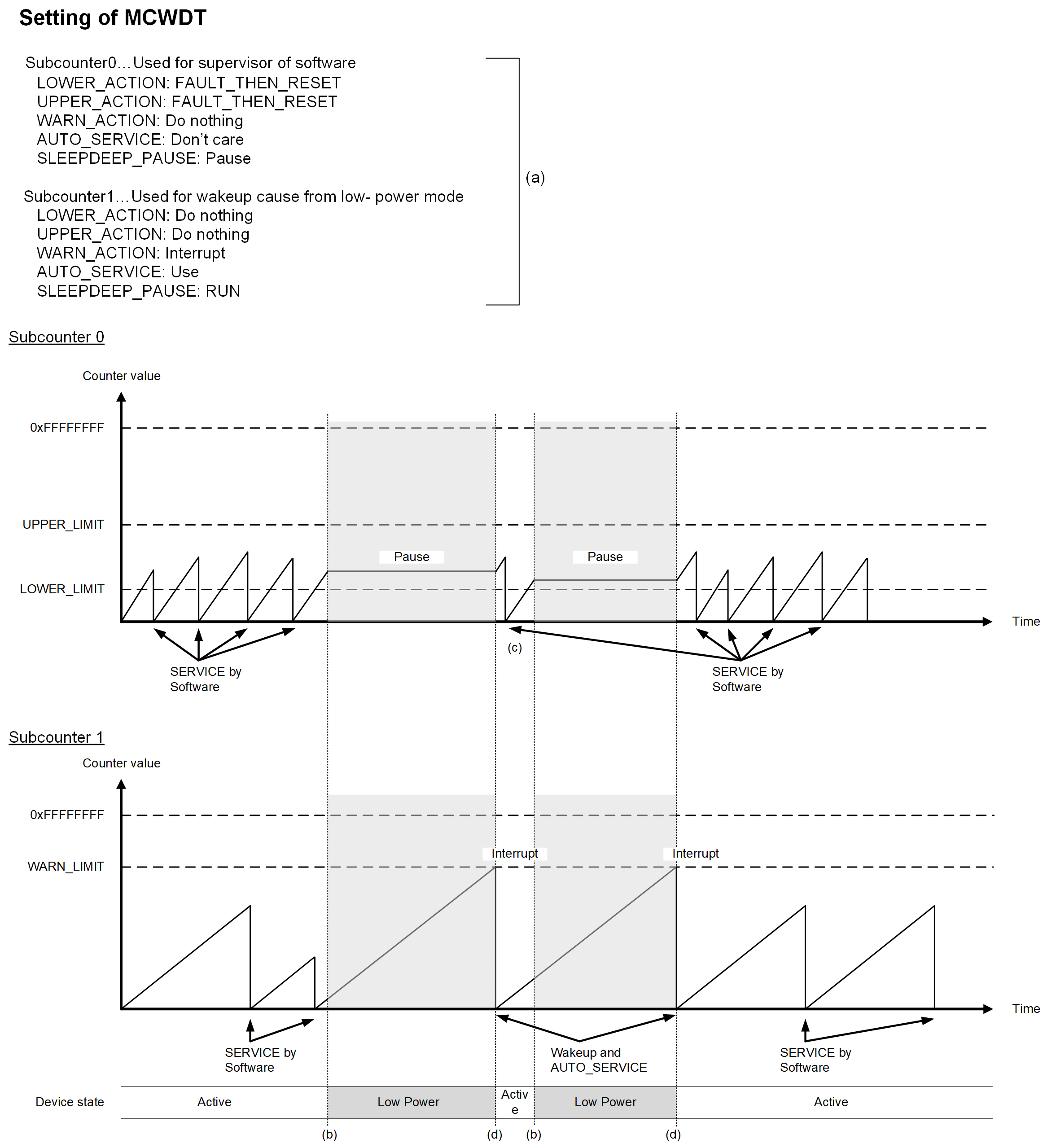
Subcounter0 is paused during low-power mode. If MCU wakes up from low-power mode, Subcounter0 resumes counting upwards.
Subcounter1 continues counting upwards during low-power mode. If counter value reaches the setting value of “WARN_LIMIT”, MCU wakes up from low-power mode. If AUTO_SERVICE setting is used, hardware resets the counter value.
Configuration and example code
Table 5 lists the parameters and Table 6 lists the functions of the configuration part in SDL for WDT settings during low-power modes.
Parameters | Description | Value |
|---|---|---|
.coreSelect | Select the CPU to be used for SleepDeepPause | CY_MCWDT_PAUSED_BY_NO_CORE |
.c0LowerLimit | Select the CPU to be used for SleepDeepPause | 0ul |
.c0UpperLimit | Select the CPU to be used for SleepDeepPause | 0xFFFFul |
.c0WarnLimit | Set the Subcounter0 warn limit (unsigned integer 32-bit) | MCWDT_TICKS_PER_SECOND |
.c0LowerAction | Set Subcounter0 lower action to “no action”, “fault”, or “fault then reset” | CY_MCWDT_ACTION_FAULT_THEN_RESET |
.c0UpperAction | Set Subcounter0 upper action to “no action”, “fault”, or “fault then reset” | CY_MCWDT_ACTION_FAULT_THEN_RESET |
.c0WarnAction | Set Subcounter0 warn action to “no action”, or “interrupt” | CY_MCWDT_WARN_ACTION_NONE |
.c0AutoService | Configure to automatically clear MCWDT when Subcounter0 value reaches WARN_LIMIT | CY_MCWDT_DISABLE |
.c0SleepDeepPause | Enable to pause Subcounter0 when the corresponding CPU is in DeepSleep | CY_MCWDT_ENABLE |
.c0DebugRun | Set the debugger configuration. It needs when using debugger | CY_MCWDT_ENABLE |
.c1LowerLimit | Set Subcounter1 lower limit (unsigned integer 32-bit) | 0ul |
.c1UpperLimit | Set Subcounter1 upper limit (unsigned integer 32-bit) | 0xFFFFul |
.c1WarnLimit | Set Subcounter1 warn limit (unsigned integer 32-bit) | MCWDT_TICKS_PER_SECOND |
.c1LowerAction | Set Subcounter1 lower action to “no action”, “fault”, or “fault then reset” | CY_MCWDT_ACTION_NONE |
.c1UpperAction | Set Subcounter1 upper action to “no action”, “fault”, or “fault then reset” | CY_MCWDT_ACTION_NONE |
.c1WarnAction | Set Subcounter1 warn action to “no action”, or “interrupt” | CY_MCWDT_WARN_ACTION_INT |
.c1AutoService | Configure to automatically clear MCWDT when Subcounter1 value reaches WARN_LIMIT | CY_MCWDT_ENABLE |
.c1SleepDeepPause | Enable to pause Subcounter1 when the corresponding CPU is in DeepSleep | CY_MCWDT_DISABLE |
.c1DebugRun | Set the debugger configuration (required when using debugger) | CY_MCWDT_ENABLE |
.c2ToggleBit | Select the bit to observe for a toggle | CY_MCWDT_CNT2_MONITORED_BIT15 |
.c2Action | Set Subcounter2 action to “no action” or “interrupt” | CY_MCWDT_CNT2_ACTION_NONE |
.c2SleepDeepPause | Enable to pause Subcounter2 when the corresponding CPU is in DeepSleep | CY_MCWDT_ENABLE |
.c2DebugRun | Set the debugger configuration (required when using debugger) | CY_MCWDT_ENABLE |
Functions | Description | Note |
|---|---|---|
Cy_MCWDT_DeInit() | De-initializes the MCWDT block, returns register values to their default state. | See Code Listing 3 |
Cy_MCWDT_Init() | Initializes the MCWDT block. | See Code Listing 4 |
Cy_MCWDT_Unlock() | Unlocks the MCWDT configuration registers. | See Code Listing 5 |
Cy_MCWDT_SetInterruptMask() | Writes MCWDT interrupt mask register. | See Code Listing 6 |
Cy_MCWDT_Enable() | Enables all specified counters. | See Code Listing 7 |
Cy_MCWDT_Lock() | Locks out configuration changes to all MCWDT registers. | See Code Listing 8 |
Cy_MCWDT_ClearWatchdog() | Clears the MC watchdog counter, to prevent a XRES device reset or fault. | See Code Listing 9 |
Cy_SysPm_DeepSleep() | Sets a CPU core to the DeepSleep mode | See Code Listing 10 |
Code Listing 1 demonstrates an example program to WDT wakeup operation in power mode transition. See the architecture reference manual and application note for GPIO and WDT.
The following description will help you understand the register notation of the driver part of SDL:
Base signifies the pointer to the MCWDT register base address. Counters specify the Subcounter within the MCWDT.
To improve the register setting performance, the SDL writes a complete 32-bit data to the register. Each bit field is generated and written to the register as the final 32-bit data.
tempCNT2ConfigParams.stcField.u5BITS            = config->c2ToggleBit;
               tempCNT2ConfigParams.stcField.u1ACTION          = config->c2Action;
               tempCNT2ConfigParams.stcField.u1SLEEPDEEP_PAUSE = config->c2SleepDeepPause;
               tempCNT2ConfigParams.stcField.u1DEBUG_RUN       = config->c2DebugRun;
               base->unCTR2_CONFIG.u32Register                 = tempCNT2ConfigParams.u32Register;
See cyip_srss_v2.h under hdr/rev_x/ip for more information on the union and structure representation of registers.
Code Listing 1 Example to WDT wakeup operation in power mode transition
int main(void)
{
    Cy_SysInt_SetSystemIrqVector(srss_interrupt_mcwdt_1_IRQn, irqMCWDT1Handler); /*Assign MCWDT interrupt*/
    :
    /*MCWDT configuration See (a) of Figure  6.
            See Code Listing 3, Code Listing 4, Code Listing 5, Code Listing 6, Code Listing 7, Code Listing 8
*/
    Cy_MCWDT_DeInit(MCWDT1);
    Cy_MCWDT_Init(MCWDT1, &mcwdtConfig);

    Cy_MCWDT_Unlock(MCWDT1);
    Cy_MCWDT_SetInterruptMask
(MCWDT1, CY_MCWDT_CTR_Msk);
    Cy_MCWDT_Enable(MCWDT1,
                    CY_MCWDT_CTR_Msk,
                    0ul);
    Cy_MCWDT_Lock(MCWDT1);

    /* Put the system to DeeSleep */
    /*See (b) of Figure  6. Set to the DeepSleep mode. See Code Listing 10*/
    Cy_SysPm_DeepSleep(CY_SYSPM_WAIT_FOR_INTERRUPT);

    for(;;)
    {
        /* Clear Watchdog counter 0 */
        /*Clears the MCWD counter See (d) of Figure  6.  See Code Listing 9*/
        Cy_MCWDT_ClearWatchdog(MCWDT1, CY_MCWDT_COUNTER0);

        while( tFlag == 0ul );
        tFlag = 0ul;
        /*See (b) of  Figure  6.  See Code Listing 10*/
        Cy_SysPm_DeepSleep(CY_SYSPM_WAIT_FOR_INTERRUPT);
    }
}
Code Listing 2 MCWDT configuration
/**
 * \var cy_stc_mcwdt_config_t mcwdtConfig
 * \brief MCWDT configuration
 */
 cy_stc_mcwdt_config_t mcwdtConfig = /*Configure MCWDT parameter*/
{
    .coreSelect       = CY_MCWDT_PAUSED_BY_NO_CORE,
    .c0LowerLimit     = 0ul,
    .c0UpperLimit     = 0xFFFFul,
    .c0WarnLimit      = MCWDT_TICKS_PER_SECOND,  /* 1 sec, ignored */
    .c0LowerAction    = CY_MCWDT_ACTION_FAULT_THEN_RESET,
    .c0UpperAction    = CY_MCWDT_ACTION_FAULT_THEN_RESET,
    .c0WarnAction     = CY_MCWDT_WARN_ACTION_NONE,
    .c0AutoService    = CY_MCWDT_DISABLE,
    .c0SleepDeepPause = CY_MCWDT_ENABLE,
    .c0DebugRun       = CY_MCWDT_ENABLE,
    .c1LowerLimit     = 0ul,
    .c1UpperLimit     = 0xFFFFul,
    .c1WarnLimit      = MCWDT_TICKS_PER_SECOND, /* 1 sec */
    .c1LowerAction    = CY_MCWDT_ACTION_NONE,
    .c1UpperAction    = CY_MCWDT_ACTION_NONE,
    .c1WarnAction     = CY_MCWDT_WARN_ACTION_INT,
    .c1AutoService    = CY_MCWDT_ENABLE,
    .c1SleepDeepPause = CY_MCWDT_DISABLE,
    .c1DebugRun       = CY_MCWDT_ENABLE,
    .c2ToggleBit      = CY_MCWDT_CNT2_MONITORED_BIT15,
    .c2Action         = CY_MCWDT_CNT2_ACTION_NONE,
    .c2SleepDeepPause = CY_MCWDT_ENABLE,
    .c2DebugRun       = CY_MCWDT_ENABLE,
};
Code Listing 3 Cy_MCWDT_DeInit() function
/* De-initializes the MCWDT block, returns register values to their default state./*

void Cy_MCWDT_DeInit(volatile stc_MCWDT_t *base)
{
    Cy_MCWDT_Unlock(base);

    // disable all counter
    for(uint32_t loop = 0ul; loop < CY_MCWDT_NUM_OF_SUBCOUNTER; loop++)
    {
        base->CTR[loop].unCTL.u32Register = 0ul;
    }
    base->unCTR2_CTL.u32Register    = 0ul;

    for(uint32_t loop = 0ul; loop < CY_MCWDT_NUM_OF_SUBCOUNTER; loop++)
    {
        while(base->CTR[loop].unCTL.u32Register != 0x0ul); // wait until enabled bit become 1
        base->CTR[loop].unLOWER_LIMIT.u32Register = 0x0ul;
        base->CTR[loop].unUPPER_LIMIT.u32Register = 0x0ul;
        base->CTR[loop].unWARN_LIMIT.u32Register  = 0x0ul;
        base->CTR[loop].unCONFIG.u32Register      = 0x0ul;
        base->CTR[loop].unCNT.u32Register         = 0x0ul;
    }

    while(base->unCTR2_CNT.u32Register != 0ul); // wait until enabled bit become 1
    base->unCPU_SELECT.u32Register  = 0ul;
    base->unCTR2_CONFIG.u32Register = 0ul;
    base->unSERVICE.u32Register     = 0x00000003ul;
    base->unINTR.u32Register        = 0xFFFFFFFFul;
    base->unINTR_MASK.u32Register   = 0ul;

    Cy_MCWDT_Lock(base);
}
Code Listing 4 Cy_MCWDT_Init() function
/* Initializes the MCWDT block.*/

cy_en_mcwdt_status_t Cy_MCWDT_Init(volatile stc_MCWDT_t *base, cy_stc_mcwdt_config_t const *config)
{
    cy_en_mcwdt_status_t ret = CY_MCWDT_BAD_PARAM;
    if ((base != NULL) && (config != NULL))
    {
        Cy_MCWDT_Unlock(base);
        un_MCWDT_CTR_CONFIG_t  tempConfigParams     = { 0ul };
        un_MCWDT_CTR2_CONFIG_t tempCNT2ConfigParams = { 0ul };

        base->unCPU_SELECT.u32Register                     = config->coreSelect;
        base->CTR[0].unLOWER_LIMIT.stcField.u16LOWER_LIMIT = config->c0LowerLimit;
        base->CTR[0].unUPPER_LIMIT.stcField.u16UPPER_LIMIT = config->c0UpperLimit;
        base->CTR[0].unWARN_LIMIT.stcField.u16WARN_LIMIT   = config->c0WarnLimit;
        tempConfigParams.stcField.u2LOWER_ACTION           = config->c0LowerAction;
        tempConfigParams.stcField.u2UPPER_ACTION           = config->c0UpperAction;
        tempConfigParams.stcField.u1WARN_ACTION            = config->c0WarnAction;
        tempConfigParams.stcField.u1AUTO_SERVICE           = config->c0AutoService;
        tempConfigParams.stcField.u1SLEEPDEEP_PAUSE        = config->c0SleepDeepPause;
        tempConfigParams.stcField.u1DEBUG_RUN              = config->c0DebugRun;
        base->CTR[0].unCONFIG.u32Register                  = tempConfigParams.u32Register;

        base->CTR[1].unLOWER_LIMIT.stcField.u16LOWER_LIMIT = config->c1LowerLimit;
        base->CTR[1].unUPPER_LIMIT.stcField.u16UPPER_LIMIT = config->c1UpperLimit;
        base->CTR[1].unWARN_LIMIT.stcField.u16WARN_LIMIT   = config->c1WarnLimit;
        tempConfigParams.stcField.u2LOWER_ACTION           = config->c1LowerAction;
        tempConfigParams.stcField.u2UPPER_ACTION           = config->c1UpperAction;
        tempConfigParams.stcField.u1WARN_ACTION            = config->c1WarnAction;
        tempConfigParams.stcField.u1AUTO_SERVICE           = config->c1AutoService;
        tempConfigParams.stcField.u1SLEEPDEEP_PAUSE        = config->c1SleepDeepPause;
        tempConfigParams.stcField.u1DEBUG_RUN              = config->c1DebugRun;
        base->CTR[1].unCONFIG.u32Register                  = tempConfigParams.u32Register;

        tempCNT2ConfigParams.stcField.u5BITS            = config->c2ToggleBit;
        tempCNT2ConfigParams.stcField.u1ACTION          = config->c2Action;
        tempCNT2ConfigParams.stcField.u1SLEEPDEEP_PAUSE = config->c2SleepDeepPause;
        tempCNT2ConfigParams.stcField.u1DEBUG_RUN       = config->c2DebugRun;
        base->unCTR2_CONFIG.u32Register                 = tempCNT2ConfigParams.u32Register;

        Cy_MCWDT_Lock(base);

        ret = CY_MCWDT_SUCCESS;
    }

    return (ret);
}
Code Listing 5 Cy_MCWDT_Unlock() function
/* Unlocks the MCWDT configuration registers.*/

STATIC_INLINE void Cy_MCWDT_Unlock(volatile stc_MCWDT_t *base)
{
    uint32_t interruptState;

    interruptState = Cy_SysLib_EnterCriticalSection();

    base->unLOCK.stcField.u2MCWDT_LOCK = CY_MCWDT_LOCK_CLR0;
    base->unLOCK.stcField.u2MCWDT_LOCK = CY_MCWDT_LOCK_CLR1;

    Cy_SysLib_ExitCriticalSection(interruptState);
}
Code Listing 6 Cy_MCWDT_SetInterruptMask() function
/* Writes MCWDT interrupt mask register.*/

__STATIC_INLINE void Cy_MCWDT_SetInterruptMask(volatile stc_MCWDT_t *base, uint32_t counters)
{
    if (counters & CY_MCWDT_CTR0)
    {
        base->unINTR_MASK.stcField.u1CTR0_INT = 1ul;
    }
    if (counters & CY_MCWDT_CTR1)
    {
        base->unINTR_MASK.stcField.u1CTR1_INT = 1ul;
    }
    if (counters & CY_MCWDT_CTR2)
    {
        base->unINTR_MASK.stcField.u1CTR2_INT = 1ul;
    }
}
Code Listing 7 Cy_MCWDT_Enable() function
/* Enables all specified counters. */

__STATIC_INLINE void Cy_MCWDT_Enable(volatile stc_MCWDT_t *base, uint32_t counters, uint16_t waitUs)
{
    if (counters & CY_MCWDT_CTR0)
    {
        base->CTR[0].unCTL.stcField.u1ENABLE = 1ul;
    }
    if (counters & CY_MCWDT_CTR1)
    {
        base->CTR[1].unCTL.stcField.u1ENABLE = 1ul;
    }
    if (counters & CY_MCWDT_CTR2)
    {
        base->unCTR2_CTL.stcField.u1ENABLE = 1ul;
    }
    Cy_SysLib_DelayUs(waitUs);
}
Code Listing 8 Cy_MCWDT_Lock() function
/* Locks out configuration changes to all MCWDT registers. */
__STATIC_INLINE void Cy_MCWDT_Lock(volatile stc_MCWDT_t *base)
{
    uint32_t interruptState;

    interruptState = Cy_SysLib_EnterCriticalSection();

    base->unLOCK.stcField.u2MCWDT_LOCK = CY_MCWDT_LOCK_SET01;

    Cy_SysLib_ExitCriticalSection(interruptState);
}
Code Listing 9 Cy_MCWDT_ClearWatchdog() function
/* Clears the MC watchdog counter, to prevent a XRES device reset or fault. */
void Cy_MCWDT_ClearWatchdog(volatile stc_MCWDT_t *base, cy_en_mcwdtctr_t counter)
{
    Cy_MCWDT_Unlock(base);
    Cy_MCWDT_ResetCounters(base, (1u << (uint8_t)counter), 0u);
    Cy_MCWDT_Lock(base);
}
Code Listing 10 Cy_SysPm_DeepSleep() function
/* Sets a CPU core to the DeepSleep mode */
cy_en_syspm_status_t Cy_SysPm_DeepSleep(cy_en_syspm_waitfor_t waitFor)
{
    uint32_t interruptState;
    cy_en_syspm_status_t retVal = CY_SYSPM_SUCCESS;

    /* Call the registered callback functions with
    * the CY_SYSPM_CHECK_READY parameter.
    */
    if(0u != currentRegisteredCallbacksNumber)
    {
        retVal = Cy_SysPm_ExecuteCallback(CY_SYSPM_DEEPSLEEP, CY_SYSPM_CHECK_READY);
    }

    /* The device (core) can switch into the deep sleep power mode only when
    *  all executed registered callback functions with the CY_SYSPM_CHECK_READY
    *  parameter returned CY_SYSPM_SUCCESS.
    */
    if(retVal == CY_SYSPM_SUCCESS)
    {
        /* Call the registered callback functions with the CY_SYSPM_BEFORE_TRANSITION
        * parameter. The return value is ignored.
        */
        interruptState = Cy_SysLib_EnterCriticalSection();
        if(0u != currentRegisteredCallbacksNumber)
        {
            (void) Cy_SysPm_ExecuteCallback(CY_SYSPM_DEEPSLEEP, CY_SYSPM_BEFORE_ENTER);
        }

    #if(0u != CY_CPU_CORTEX_M0P)

        /* The CPU enters the deep sleep mode upon execution of WFI/WFE */
        SCB->SCR |= SCB_SCR_SLEEPDEEP_Msk;

        if(waitFor != CY_SYSPM_WAIT_FOR_EVENT)
        {
            __WFI();
        }
        else
        {
            __WFE();
        }
    #else

        /* Repeat WFI/WFE instructions if wake up was not intended.
        *  Cypress Ticket #272909
        */
        do
        {
            SCB->SCR |= SCB_SCR_SLEEPDEEP_Msk;

            if(waitFor != CY_SYSPM_WAIT_FOR_EVENT)
            {
                __WFI();
            }
            else
            {
                __WFE();
            }
        } while (0); //rmkn _FLD2VAL(CPUSS_CM4_PWR_CTL_PWR_MODE, CPUSS->unCM4_PWR_CTL.u32Register) == CY_SYSPM_CM4_PWR_CTL_PWR_MODE_RETAINED);

    #endif /* (0u != CY_CPU_CORTEX_M0P) */

        Cy_SysLib_ExitCriticalSection(interruptState);

        /* Call the registered callback functions with the CY_SYSPM_AFTER_TRANSITION
        *  parameter. The return value is ignored.
        */
        if(0u != currentRegisteredCallbacksNumber)
        {
            (void) Cy_SysPm_ExecuteCallback(CY_SYSPM_DEEPSLEEP, CY_SYSPM_AFTER_EXIT);
        }
    }
    else
    {
        /* Execute callback functions with the CY_SYSPM_CHECK_FAIL parameter to
        * undo everything done in the callback with the CY_SYSPM_CHECK_READY
        * parameter. The return value is ignored.
        */
        (void) Cy_SysPm_ExecuteCallback(CY_SYSPM_DEEPSLEEP, CY_SYSPM_CHECK_FAIL);
        retVal = CY_SYSPM_FAIL;
    }
    return retVal;
}
Cyclic wakeup operation
Cyclic wakeup operation is an intermittent MCU operation. For example, when the electronic control unit (ECU) is in Sleep mode, MCU cyclically enters DeepSleep mode and wakes up. This operation is intended to minimize the average power consumption in an application. This section describes an implementation example of cyclic wakeup operation by using TRAVEO™ T2G family MCUs.
Usage example of cyclic wakeup
Figure 7 shows an example of a user system. MCU controls the GPIO and ADC for monitoring external devices, sensors, and so on.
Figure 7.
Block diagram of an example user system
The external device is connected to MCU via GPIO. The external device wakes up the sensor by the control signal from the MCU. The sensor outputs are connected to the ADC of the MCU.
However, the sensor generally requires a stabilization wait time to correctly output after wakeup.
Therefore, the MCU outputs the sensor wakeup signal to the external device, and activates ADC after a certain time to convert the sensor signal. For generating these two different timings, two timer interrupts (Comp0 and Comp1) of the event generator are used. In this case, Comp0 is used as a trigger for ADC activation, and Comp1 is used for CPU wakeup.
Cyclic wakeup operation
Figure 8 shows the concept of the cyclic wakeup operation. TRAVEO™ T2G device cyclically wakes up to check the external sensor information when the ECU enters Sleep mode.
Figure 8.
Cyclic wakeup operation
(0) After a reset, TRAVEO™ T2G enters Active mode and operates the user software.
(1) The CPU core configures and runs the event generator with the 32.768 kHz low-frequency oscillator.
(The source clock of the event generator can be selected from ILO0, ILO1, and WCO.)
(2) TRAVEO™ T2G enters DeepSleep mode; the CPU core goes to DeepSleep state.
(3) If the counter value of the event generator matches Comp1, the Comp1 trigger wakes up the CPU core.
(4) The CPU (software) controls the GPIO to output a wakeup trigger activation for external devices.
(5) Comp0 trigger starts an ADC range comparison.
(6) The CPU (software) observes ADC results.
(7) The CPU (software) controls the GPIO.
[If ADC results of range detection are in range, ECU continues to run cyclic wakeup operation.]
(8) The CPU (software) restarts the event generator. The CPU goes back to DeepSleep mode. [Go to (2)]
[If ADC results of range detection are out of range, ECU exits from cyclic wakeup operation.]
(9) CPU (software) restarts the operation of the ECU system.
For more details on event generator, ADC, GPIO, and clock, see the architecture reference manual .
Flowchart of cyclic wakeup operation
Figure 9.
Flowchart of cyclic wakeup operation
Note:
The gray boxes indicate hardware operation in Figure 9 . Therefore, processing with software is not required.
Configuration and example code
Table 7 lists the parameters and Table 8 lists the functions of the configuration part in SDL for cyclic wakeup operation.
Parameters | Description | Value |
|---|---|---|
.frequencyRef | clk_ref | 8000000 |
.frequencyLf | clk_lf | 32000 |
.frequencyTick | Event generator clock (clk_ref_div) | 1000000 (Setting 1,000,000 Hz) |
.ratioControlMode | Event generator ratio control mode | CY_EVTGEN_RATIO_CONTROL_HW |
.ratioValueDynamicMode | Event generator dynamic mode | CY_EVTGEN_RATIO_DYNAMIC_MODE0 |
.functionalitySelection | Event generator select functionality | CY_EVTGEN_DEEPSLEEP_FUNCTIONALITY |
.triggerOutEdge | Event generator trigger | CY_EVTGEN_EDGE_SENSITIVE |
.valueDeepSleepComparator | Wakes up the CPU after time | 1000000 (1 sec) |
.valueActiveComparator | Triggers ADC after time | 1500000 (1.5 sec) |
.userIsr | Event generator struct handler | NULL |
Functions | Description | Remarks |
|---|---|---|
AdcIntHandler() | Interrupt handler for ADC | See Code Listing 11 |
irqEVTGEN_sleep() | Interrupt setting for event generator | See Code Listing 11 |
Cy_Evtgen_ClearStructInterruptDeepSleep() | Clears the DeepSleep interrupt factor of the corresponding structure | See Code Listing 12 |
Cy_Evtgen_DeinitializeCompStruct() | Deinitializes the event generator structure | See Code Listing 13 |
Cy_Evtgen_Deinitialize() | Deinitializes the event generator | See Code Listing 14 |
Cy_Evtgen_Initialize() | Initializes the event generator | See Code Listing 15 |
Cy_Evtgen_InitializeCompStruct() | Initializes the comparator structure | See Code Listing 16 |
Cy_SysInt_SetSystemIrqVector() | Changes the user ISR vector for the system interrupt | See Code Listing 18 |
Cy_SysPm_DeepSleep() | Sets a CPU core to the DeepSleep mode | See Code Listing 17 |
Code Listing 11 demonstrates an example program to cyclic wakeup operation. See the architecture reference manual and application note for GPIO and ADC.
Code Listing 11 Example of cyclic wakeup operation
/* Eventgenerator Configration */

const cy_stc_evtgen_config_t evtgenTestConfig =
{
  #else
    .frequencyRef          = 8000000,  //  clk_ref = clk_hf1
    .frequencyLf           = 32000,    // clk_lf = 32,000 for silicon
  #endif
    .frequencyTick         = 1000000,  // Setting 1,000,000 Hz for event generator clock
    .ratioControlMode      = CY_EVTGEN_RATIO_CONTROL_HW,
    .ratioValueDynamicMode = CY_EVTGEN_RATIO_DYNAMIC_MODE0,
};


const cy_stc_evtgen_struct_config_t evtgenTestStructureConfig =
{
    .functionalitySelection   = CY_EVTGEN_DEEPSLEEP_FUNCTIONALITY,
    .triggerOutEdge           = CY_EVTGEN_EDGE_SENSITIVE,
    .valueDeepSleepComparator = 1000000, // It wake CPU up after 1s.
    .valueActiveComparator    = 1500000, // It triggers ADC after 1.5s.
    .userIsr = NULL,
};

/* See (d) of Figure  9.  Interrupt handler for ADC */
void AdcIntHandler(void)
{
   cy_stc_adc_interrupt_source_t intrSource = { false };
    /* Get the result(s) */
    Cy_Adc_Channel_GetResult(&BB_POTI_ANALOG_MACRO->CH[ADC_LOGICAL_CHANNEL], &resultBuff[resultIdx], &statusBuff[resultIdx]);
    resultIdx = (resultIdx + 1) % (sizeof(resultBuff) / sizeof(resultBuff[0]));
    /* Clear inerrupt source */
    Cy_Adc_Channel_GetInterruptMaskedStatus(&BB_POTI_ANALOG_MACRO->CH[ADC_LOGICAL_CHANNEL], &intrSource);
    Cy_Adc_Channel_ClearInterruptStatus(&BB_POTI_ANALOG_MACRO->CH[ADC_LOGICAL_CHANNEL], &intrSource);

    adcCompletedFlag = 1;
}

void irqEVTGEN_sleep(void)
{
/* See (c) of Figure  9. See Code Listing 12 */
    Cy_Evtgen_ClearStructInterruptDeepSleep(EVTGEN0,0);
}

int main(void)
{
:
/* Event generator configuration.See (a) of Figure  9.  */
    /*******************************************/
    /*        Deinitialize peripherals         */
    /*******************************************/
    Cy_Evtgen_DeinitializeCompStruct(EVTGEN0, 0);  /* See Code Listing 13 */
            Cy_Evtgen_Deinitialize(EVTGEN0);   /* See Code Listing 14 */

    /*******************************************/
    /*  Initialize and start Event generator   */
    /*******************************************/
    Cy_Evtgen_Initialize(EVTGEN0,&evtgenTestConfig);  /* See Code Listing 15 */

    /*******************************************/
    /*  Initialize comparator structure 0      */
    /*******************************************/
    Cy_Evtgen_InitializeCompStruct(EVTGEN0, 0,   /* See Code Listing 16 */
&evtgenTestStructureConfig, &evtgenStruct0Context);

    /* Register ADC interrupt handler and enable interrupt */
    Cy_SysInt_SetSystemIrqVector(irq_cfg_adc.sysIntSrc, AdcIntHandler);

    /* Put the system to DeeSleep */
    Cy_SysPm_DeepSleep((cy_en_syspm_waitfor_t)CY_SYSPM_WAIT_FOR_INTERRUPT);

/* See (b) of Figure  9. Set to the DeepSleep mode. See Code Listing 17 */
    for(;;)
    {
        while(adcCompletedFlag == 0);
        adcCompletedFlag = 0;

        Cy_Evtgen_DeinitializeCompStruct(EVTGEN0, 0);
        Cy_Evtgen_InitializeCompStruct(EVTGEN0, 0, &evtgenTestStructureConfig, &evtgenStruct0Context);
        /* Put the system to DeeSleep */
        Cy_SysPm_DeepSleep((cy_en_syspm_waitfor_t)CY_SYSPM_WAIT_FOR_INTERRUPT);
    }

}
Code Listing 12 Cy_Evtgen_ClearStructInterruptDeepSleep() function
/* Clear DeepSleep interrupt factor of corresponding structure */
__STATIC_INLINE void Cy_Evtgen_ClearStructInterruptDeepSleep(volatile stc_EVTGEN_t *base, uint8_t structNumber)
{
    base->unINTR_DPSLP.u32Register = ((uint32_t)1 << structNumber);

    // Dummy read. This is to wait for reflection above write operation.
    base->unINTR_DPSLP;
}
Code Listing 13 Cy_Evtgen_DeinitializeCompStruct() function
void Cy_Evtgen_DeinitializeCompStruct(volatile stc_EVTGEN_t *base, uint8_t structNum)
{
    /* Deinitialize event generator structure */
    base->COMP_STRUCT[structNum].unCOMP_CTL.u32Register = 0;
    base->COMP_STRUCT[structNum].unCOMP0.stcField.u32INT32 = 0;
    base->COMP_STRUCT[structNum].unCOMP1.stcField.u32INT32 = 0;
    evtgenContext[structNum] = NULL;
}
Code Listing 14 Cy_Evtgen_Deinitialize() function
void Cy_Evtgen_Deinitialize(volatile stc_EVTGEN_t *base)
{
    /* Deinitialize event generator */
    base->unCTL.u32Register = 0;
    base->unREF_CLOCK_CTL.u32Register = 0;
    base->unRATIO.u32Register = 0;
    base->unRATIO_CTL.u32Register = 0;
    base->unINTR_MASK.u32Register = 0;
    base->unINTR_DPSLP_MASK.u32Register = 0;
}
Code Listing 15 Cy_Evtgen_Initialize() function
cy_en_evtgendrv_status_t Cy_Evtgen_Initialize(volatile stc_EVTGEN_t *base, const cy_stc_evtgen_config_t* config)
{

/* Initialize the event generator */
uint16_t refDiv;

    un_EVTGEN_RATIO_CTL_t ratioCtl;

    /* 1. Checking input parameter valid */
    if(config == NULL)
    {
        return CY_EVTGEN_ERR;
    }

    /* 2. Initialize internal variable */
    for(uint32_t i = 0; i < EVTGEN_COMP_STRUCT_NR; i++)
    {
        evtgenContext[i] = NULL;
    }
    mapUsed = 0;

    Cy_Evtgen_Enable(base);

    /* 2. Setting divider value of clk_ref */
    refDiv = config->frequencyRef / config->frequencyTick;
    if(config->frequencyRef % config->frequencyTick != 0)
    {
        return CY_EVTGEN_ERR;
    }
    else if(refDiv > 256 || refDiv  < 1)
    {
        return CY_EVTGEN_ERR;
    }
    else
    {
        base->unREF_CLOCK_CTL.stcField.u8INT_DIV = refDiv - 1u;
    }

    /* 3. Setting ratio operation */
    if(config->ratioControlMode == CY_EVTGEN_RATIO_CONTROL_SW)
    {
        /* SW controll: setting value for ratio value should be ratio between tick_ref_div and clk_lf. */
        uint64_t temp = (uint64_t)(config->frequencyRef / refDiv) << EVTGEN_RATIO_INT16_Pos;
        temp = temp / (uint64_t)(config->frequencyLf);
        base->unRATIO.u32Register = ((uint32_t)temp) & (EVTGEN_RATIO_INT16_Msk | EVTGEN_RATIO_FRAC8_Msk);

        base->unRATIO_CTL.stcField.u1DYNAMIC = 0u;

        /* SW controll: valid bit should be set manually. */
        base->unRATIO_CTL.stcField.u1VALID = 1u; /* Set VALID bit */
    }
    else
    {
        /* HW controll: */
        ratioCtl.u32Register = base->unRATIO_CTL.u32Register;
        ratioCtl.stcField.u1DYNAMIC = 1u; /* Set Dynamic bit */
        ratioCtl.stcField.u3DYNAMIC_MODE = config->ratioValueDynamicMode; /* Set Dynamic bit */
        base->unRATIO_CTL.u32Register = ratioCtl.u32Register;

        /* Waiting until valid bit is set. */
        while(base->unRATIO_CTL.stcField.u1VALID == 0u);
    }

    /* Waiting until counter become ready. */
    while(base->unCOUNTER_STATUS.stcField.u1VALID == 0u);

    return CY_EVTGEN_OK;
}
Code Listing 16 Cy_Evtgen_InitializeCompStruct() function
cy_en_evtgendrv_status_t Cy_Evtgen_InitializeCompStruct(volatile stc_EVTGEN_t *base,
                                                        uint8_t structNum,
                                                        const cy_stc_evtgen_struct_config_t* configStruct,
                                                        cy_stc_evtgen_struct_context_t* context)
{

/* Initialize a comparator structure */

un_EVTGEN_COMP_STRUCT_COMP_CTL_t compCtr;
    uint64_t tempCounterValue;
    uint32_t savedIntrStatus;

    /* Checking input parameter valid */
    if(configStruct == NULL)
    {
        return CY_EVTGEN_ERR;
    }

    if(structNum >= EVTGEN_COMP_STRUCT_NR)
    {
        return CY_EVTGEN_ERR;
    }

    if(configStruct->functionalitySelection != CY_EVTGEN_DEEPSLEEP_FUNCTIONALITY)
    {
        if(context == NULL)
        {
            return CY_EVTGEN_ERR;
        }
        evtgenContext[structNum] = context;
        evtgenContext[structNum]->addValueForCOMP0 = configStruct->valueActiveComparator;
        evtgenContext[structNum]->userIsr = configStruct->userIsr;
        mapUsed |= 1 << structNum;
    }

    compCtr.u32Register = base->COMP_STRUCT[structNum].unCOMP_CTL.u32Register;

    if(configStruct->functionalitySelection == CY_EVTGEN_DEEPSLEEP_FUNCTIONALITY)
    {
        compCtr.stcField.u1COMP1_EN = 1u;
    }

    compCtr.stcField.u1COMP0_EN = 1u;

    compCtr.stcField.u1TR_OUT_EDGE = configStruct->triggerOutEdge;

    compCtr.stcField.u1ENABLED = 1u;

    savedIntrStatus = Cy_SysLib_EnterCriticalSection();

    tempCounterValue = (uint64_t)Cy_Evtgen_GetCounterValue(base);

    /* Setting active comparator value */
    base->COMP_STRUCT[structNum].unCOMP0.stcField.u32INT32 = (uint32_t)(tempCounterValue + (uint64_t)configStruct->valueActiveComparator);

    /* Setting deep sleep comparator value */
    if(configStruct->functionalitySelection == CY_EVTGEN_DEEPSLEEP_FUNCTIONALITY)
    {
        base->COMP_STRUCT[structNum].unCOMP1.stcField.u32INT32 = (uint32_t)(tempCounterValue + (uint64_t)configStruct->valueDeepSleepComparator);
    }

    Cy_SysLib_ExitCriticalSection(savedIntrStatus);

    /* Setting comparator struct controll parameter */
    base->COMP_STRUCT[structNum].unCOMP_CTL.u32Register = compCtr.u32Register;

    Cy_Evtgen_SetInterruptMask(base, structNum);
    if(configStruct->functionalitySelection == CY_EVTGEN_DEEPSLEEP_FUNCTIONALITY)
    {
        Cy_Evtgen_SetInterruptDeepSleepMask(base, structNum);
    }

    return CY_EVTGEN_OK;
}
Code Listing 17 Cy_SysPm_DeepSleep() function
cy_en_syspm_status_t Cy_SysPm_DeepSleep(cy_en_syspm_waitfor_t waitFor)
{

    /* Sets a CPU core to the DeepSleep  mode */
    uint32_t interruptState;
    cy_en_syspm_status_t retVal = CY_SYSPM_SUCCESS;

    /* Call the registered callback functions with
    * the CY_SYSPM_CHECK_READY parameter.
    */
    if(0u != currentRegisteredCallbacksNumber)
    {
        retVal = Cy_SysPm_ExecuteCallback(CY_SYSPM_DEEPSLEEP, CY_SYSPM_CHECK_READY);
    }

    /* The device (core) can switch into the deep sleep power mode only when
    *  all executed registered callback functions with the CY_SYSPM_CHECK_READY
    *  parameter returned CY_SYSPM_SUCCESS.
    */
    if(retVal == CY_SYSPM_SUCCESS)
    {
        /* Call the registered callback functions with the CY_SYSPM_BEFORE_TRANSITION
        * parameter. The return value is ignored.
        */
        interruptState = Cy_SysLib_EnterCriticalSection();
        if(0u != currentRegisteredCallbacksNumber)
        {
            (void) Cy_SysPm_ExecuteCallback(CY_SYSPM_DEEPSLEEP, CY_SYSPM_BEFORE_ENTER);
        }

    #if(0u != CY_CPU_CORTEX_M0P)

        /* The CPU enters the deep sleep mode upon execution of WFI/WFE */
        SCB->SCR |= SCB_SCR_SLEEPDEEP_Msk;

        if(waitFor != CY_SYSPM_WAIT_FOR_EVENT)
        {
            __WFI();
        }
        else
        {
            __WFE();
        }
    #else

        /* Repeat WFI/WFE instructions if wake up was not intended.
        *  Cypress Ticket #272909
        */
        do
        {
            SCB->SCR |= SCB_SCR_SLEEPDEEP_Msk;

            if(waitFor != CY_SYSPM_WAIT_FOR_EVENT)
            {
                __WFI();
            }
            else
            {
                __WFE();
            }
        } while (0); //rmkn _FLD2VAL(CPUSS_CM4_PWR_CTL_PWR_MODE, CPUSS->unCM4_PWR_CTL.u32Register) == CY_SYSPM_CM4_PWR_CTL_PWR_MODE_RETAINED);

    #endif /* (0u != CY_CPU_CORTEX_M0P) */

        Cy_SysLib_ExitCriticalSection(interruptState);

        /* Call the registered callback functions with the CY_SYSPM_AFTER_TRANSITION
        *  parameter. The return value is ignored.
        */
        if(0u != currentRegisteredCallbacksNumber)
        {
            (void) Cy_SysPm_ExecuteCallback(CY_SYSPM_DEEPSLEEP, CY_SYSPM_AFTER_EXIT);
        }
    }
    else
    {
        /* Execute callback functions with the CY_SYSPM_CHECK_FAIL parameter to
        * undo everything done in the callback with the CY_SYSPM_CHECK_READY
        * parameter. The return value is ignored.
        */
        (void) Cy_SysPm_ExecuteCallback(CY_SYSPM_DEEPSLEEP, CY_SYSPM_CHECK_FAIL);
        retVal = CY_SYSPM_FAIL;
    }
    return retVal;
}
Code Listing 18 C Cy_SysInt_SetSystemIrqVector() function
void  Cy_SysInt_SetSystemIrqVector(cy_en_intr_t sysIntSrc, cy_systemIntr_Handler userIsr)
{

    /* Changes the User ISR vector for the System Interrupt */
    if (Cy_SysInt_SystemIrqUserTableRamPointer != NULL)
    {
        Cy_SysInt_SystemIrqUserTableRamPointer[sysIntSrc] = userIsr;
    }
}
Usage of smart I/O in cyclic wakeup
This section describes the role of smart I/O in reducing the LPACTIVE period in cyclic wakeup operation.
As described in the beginning of the cyclic wakeup operation section, cyclic wakeup is intended to minimize the average power consumption in an application. This average consumption current is affected by the following:
DeepSleep current
LPACTIVE current
Percentage of LPACTIVE time in one period.
DeepSleep current and LPACTIVE current mostly depend on electrical specifications of HW, while the percentage of the LPACTIVE time in one period depends on the optimization of SW. Because the current consumption during LPACTIVE (several mA) is relatively much higher than in DeepSleep (several 10μA), from the SW point of view, reducing the LPACTIVE time plays an important factor in achieving a low average consumption current. To shorten the LPACTIVE period, use of Smart I/O is suggested.
In the flow of cyclic wakeup operation proposed in Figure 8 , the MCU need to wake up and configure I/O ports to turn sensors on, and wait for the sensor’s stabilization before triggering ADC conversion. If a long sensor stabilization time is required, the MCU can optionally be put in Sleep/DeepSleep again to reduce the current consumption, but this approach may make program more complex. Additionally, you should consider the transition time between different power modes.
Figure 10 shows the system configuration of this use case. GPIO is activated by smart I/O, instead of CPU as demonstrated in Figure 7 .
Figure 10.
System configuration of cyclic wakeup with smart I/O
Advantage of smart I/O implementation in cyclic wakeup
Smart I/O can be used to manipulate I/O during DeepSleep mode. This can eliminate the unnecessary LPACTIVE time CPU spends to activate I/O especially when the CPU must wait for a long time for the sensor to stabilize.
The internal logic of smart I/O includes three-input lookup table (LUTs) and data unit (DU) among other components. DU acts as a counter with count up/down and reload function. By setting the data unit and LUTs properly, we can create a circuit that delays GPIO from outputting high with desired latency.
As shown in Figure 11 , because smart I/O can operate in DeepSleep, you can use it to activate GPIO while the CPU is in DeepSleep mode.
Figure 11.
Smart I/O-based cyclic wakeup operation
Smart I/O configuration in cyclic wakeup
The data unit (DU) can be used as a counter to delay “H” output. However, the DU is only 8-bit counter. During DeepSleep, because the source clock of smart I/O is ILO with frequency of 32 kHz, the DU can count for maximum interval as follows:
Therefore, for applications that require cyclic wakeup period larger than 8 ms, you need extra bits for the counter.
Therefore, for this example, an 11-bit timer equivalent circuitry by smart I/O called “sensor activation circuitry” is implemented. An 11-bit counter equivalent circuitry can generate delay up to 32 ms. Figure 12 shows the operation of the circuitry. Here, ‘DAT’ is the upper limit of the DU. DAT is configured by the SMARTIO_PRTx_DATA register. A single clock pulse is output at the data unit tr_out when the count value is equal to DAT.
Figure 12.
Operation of sensor activation circuitry

In this use case, the circuitry receives one signal from HSIOM named the “sensor_io_clr” signal, with active HIGH, which is used to clear the output of LUT3[1], i.e., the sensor activation output. The following I/O port and HSIOM signal are used:
smartio_data[1] = sensor_io (to I/O port, i.e., external sensor activation port)
chip_data[1] = sensor_io_clr (from HSIOM, manipulated by the CPU to clear ‘sensor_io’)
Figure 13 shows the connection and functional logic of each LUT3 and DU in this circuitry.
Figure 13.
Logical example of a sensor activation circuitry
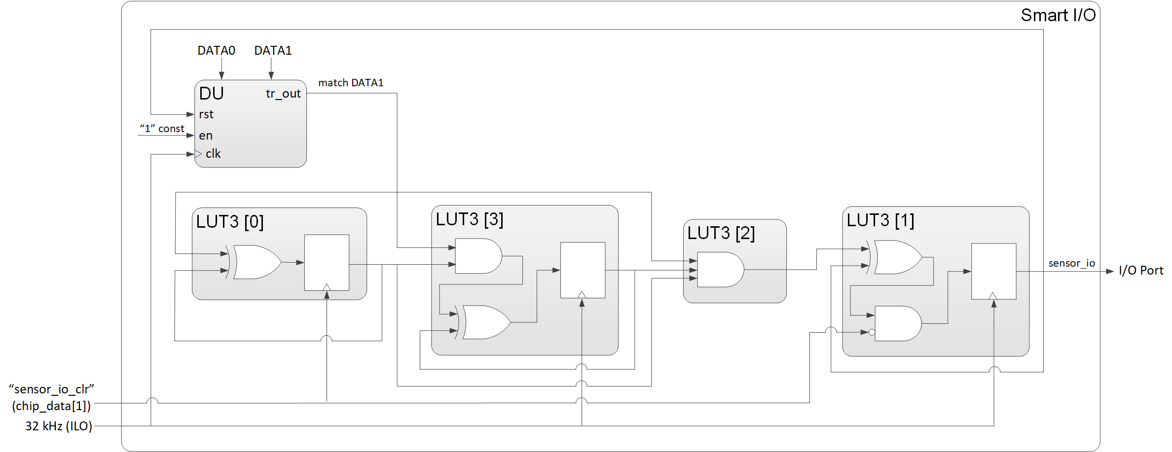
The data unit operates in INCR_WRAP mode. This mode increments the data by 1 from an initial value (DATA 0) until it reaches a final value (DATA 1). When the count value matches the final value, it wraps around to DATA 0.
In this circuitry, the data unit carries the lower 8 bits of the 11-bit counter, LUT3[0], LUT3[1], LUT3[3] stands for the 9th, 10 th , and 11th bit of the 11-bit counter. The output of LUT3[1], i.e., the 11th bit of the counter, is connected to the GPIO port to activate the external sensor. Figure 14 shows the signal path in this use case.
Figure 14.
Signal path of sensor activation circuitry
Table 9 , Table 10 , Table 11 , and Table 12 , show the truth table of each LUT3. The bold in the table indicate an invalid pattern.
Tr2_in | Tr1_in | Tr0_in | Tr_out | |
|---|---|---|---|---|
LUT3[0] out | LUT3[0] out | DU tr_out | ||
0 | 0 | 0 | 0 | |
0 | 0 | 1 | 1 | |
0 | 1 | 0 | 0 | |
0 | 1 | 1 | 0 | |
1 | 0 | 0 | 0 | |
1 | 0 | 1 | 0 | |
1 | 1 | 0 | 1 | |
1 | 1 | 1 | 0 | |
Tr2_in | Tr1_in | Tr0_in | Tr_out | |
|---|---|---|---|---|
LUT3[1] out | LUT3[0] out | DU tr_out | ||
0 | 0 | 0 | 0 | |
0 | 0 | 1 | 0 | |
0 | 1 | 0 | 1 | |
0 | 1 | 1 | 0 | |
1 | 0 | 0 | 1 | |
1 | 0 | 1 | 0 | |
1 | 1 | 0 | 1 | |
1 | 1 | 1 | 0 | |
Tr2_in | Tr1_in | Tr0_in | Tr_out | |
|---|---|---|---|---|
LUT3[1] out | LUT3[0] out | DU tr_out | ||
0 | 0 | 0 | 0 | |
0 | 0 | 1 | 0 | |
0 | 1 | 0 | 0 | |
0 | 1 | 1 | 0 | |
1 | 0 | 0 | 0 | |
1 | 0 | 1 | 0 | |
1 | 1 | 0 | 0 | |
1 | 1 | 1 | 1 | |
Tr0_in | Tr1_in | Tr2_in | Tr_out | |
|---|---|---|---|---|
LUT3[3] out | LUT3[2] out | CHIP_ DATA[0] | ||
0 | 0 | 0 | 0 | |
0 | 0 | 1 | 0 | |
0 | 1 | 0 | 0 | |
0 | 1 | 1 | 1 | |
1 | 0 | 0 | 1 | |
1 | 0 | 1 | 1 | |
1 | 1 | 0 | 1 | |
1 | 1 | 1 | 0 | |
The H output delayed by the sensor activation circuitry can be calculated as follows:
Therefore, you can configure DAT1 and DAT0 (usually set to ‘0’) to satisfy the sensor stabilization waiting time as in the rough estimation as follows:
For example, if=32 [ms], you can configure DAT0 = 0, DAT1 = 0xFD to make
Sensor activation circuitry in cyclic wakeup operation
Using the sensor activation circuitry constructed in the previous section, the operation of cyclic wakeup can be enhanced as shown in Figure 15 .
Figure 15.
Cyclic wakeup operation with smart I/O usage
Note:
The gray box in the flowchart indicates a hardware operation. Therefore, processing with software is not required.
The GPIO is activated by smart I/O while the CPU is still in DeepSleep mode and the sensor’s stabilization time can be satisfied just by adjusting DAT0 and DAT1 properly. The behavior of the GPIO is now isolated from the operation of the CPU; this makes the software flow less complex.
For example, the CPU does not need to go to Sleep mode after activating the GPIO to cut back the current consumption if a long sensor waiting time is required.
Configuration and example code
Table 13 lists the parameters and Table 14 lists the functions of the configuration part in SDL for smart I/O in cyclic wakeup.
Parameters | Description | Value |
|---|---|---|
.sysIntSrc | Interrupt setting for event generator | evtgen_0_interrupt_dpslp_IRQn |
.intIdx | CPUIntIdx4_IRQn | |
.isEnabled | true | |
.frequencyRef | clk_ref | 8000000ul |
.frequencyLf | clk_lf | 32000ul |
.frequencyTick | Event generator clock (clk_ref_div) | 32000ul |
.ratioControlMode | Event generator ratio control mode | CY_EVTGEN_RATIO_CONTROL_SW |
.ratioValueDynamicMode | Event generator dynamic mode | CY_EVTGEN_RATIO_DYNAMIC_MODE0 |
.functionalitySelection | Event generator select functionality | CY_EVTGEN_DEEPSLEEP_FUNCTIONALITY |
.triggerOutEdge | Event generator trigger | CY_EVTGEN_EDGE_SENSITIVE |
.valueDeepSleepComparator | Initializes comparator structure | DPSLP_COMP_VAL |
.valueActiveComparator | Initializes comparator structure | ACTIVE_COMP_VAL |
lutCfgLut0.opcode | Configures LUT3[0] operation mode setting | CY_SMARTIO_LUTOPC_GATED_OUT |
lutCfgLut0.lutMap | Configures LUT3[0] output pattern setting | 0x42ul |
lutCfgLut0.tr0 | Configures LUT3[0] tr0 input | CY_SMARTIO_LUTTR_DU_OUT |
lutCfgLut0.tr1 | Configures LUT3[0] tr1 input | CY_SMARTIO_LUTTR_LUT0_OUT |
lutCfgLut0.tr2 | Configures LUT3[0] tr2 input | CY_SMARTIO_LUTTR_LUT0_OUT |
lutCfgLut3.opcode | Configures LUT3[3] operation mode setting | CY_SMARTIO_LUTOPC_GATED_OUT |
lutCfgLut3.lutMap | Configures LUT3[3] output pattern setting | 0x78ul |
lutCfgLut3.tr0 | Configures LUT3[3] tr0 input | CY_SMARTIO_LUTTR_DU_OUT |
lutCfgLut3.tr1 | Configures LUT3[3] tr1 input | CY_SMARTIO_LUTTR_LUT0_OUT |
lutCfgLut3.tr2 | Configures LUT3[3] tr2 input | CY_SMARTIO_LUTTR_LUT3_OUT |
lutCfgLut2.opcode | Configures LUT3[2] operation mode setting | CY_SMARTIO_LUTOPC_COMB |
lutCfgLut2.lutMap | Configures LUT3[2] output pattern setting | 0x80ul |
lutCfgLut2.tr0 | Configures LUT3[2] tr0 input | CY_SMARTIO_LUTTR_DU_OUT |
lutCfgLut2.tr1 | Configures LUT3[2] tr1 input | CY_SMARTIO_LUTTR_LUT0_OUT |
lutCfgLut2.tr2 | Configures LUT3[2] tr2 input | CY_SMARTIO_LUTTR_LUT3_OUT |
lutCfgLut1.opcode | Configures LUT3[1] operation mode setting | CY_SMARTIO_LUTOPC_GATED_OUT |
lutCfgLut1.lutMap | Configures LUT3[1] output pattern setting | 0x54ul |
lutCfgLut1.tr0 | Configures LUT3[1] tr0 input | CY_SMARTIO_LUTTR_CHIP1 |
lutCfgLut1.tr1 | Configures LUT3[1] tr1 input | CY_SMARTIO_LUTTR_LUT1_OUT |
lutCfgLut1.tr2 | Configures LUT3[1] tr2 input | CY_SMARTIO_LUTTR_LUT2_OUT |
lutCfgDu.tr0 | Configures DU input trigger 0 source selection | CY_SMARTIO_DUTR_LUT1_OUT |
lutCfgDu.tr1 | Configures DU input trigger 1 source selection | CY_SMARTIO_DUTR_ONE |
lutCfgDu.data0 | DU input DATA0 source selection | CY_SMARTIO_DUDATA_ZERO |
lutCfgDu.data1 | DU input DATA1 source selection | CY_SMARTIO_DUDATA_DATAREG |
lutCfgDu.opcode | DU opcode | CY_SMARTIO_DUOPC_INCR_WRAP |
lutCfgDu.size | DU width size is 8 | CY_SMARTIO_DUSIZE_8 |
lutCfgDu.dataReg | DU DATA register value | 0xFCul |
Functions | Description | Remarks |
|---|---|---|
CyclicWakeUp_SystemUpdate() | SystemUpdate for cyclic wakeup | See Code Listing 21 |
CyclicWakeUp_Operation() | Cyclic wakeup function | See Code Listing 22 |
Init_SmartIO() | Smart I/O module initialization | See Code Listing 23 |
Cy_SmartIO_Enable() | Enables smart I/O | See Code Listing 24 |
Init_SmartIO_Cfg() | Configures smart I/O | See Code Listing 25 |
Cy_SmartIO_Deinit() | Resets the smart I/O to default values | See Code Listing 26 |
Cy_GPIO_Inv() | Sets a pin output logic state to the inverse of the current output logic state | See Code Listing 27 |
Code Listing 19 demonstrates an example program to smart I/O in cyclic wakeup operation. See the architecture reference manual and application note for GPIO, ADC, and smart I/O.
Code Listing 19 Example of usage of smart I/O in cyclic wakeup operation
int main(void)
{
:
  CyclicWakeUp_SystemUpdate();  /* SystemUpdate for Cyclic wakeup See Code Listing 21 */

  Init_SmartIO();   /* Smart IO module initialization See Code Listing 23 */

  Cy_SmartIO_Enable(SMART_IO_PORT);   /* Configures Smart I/O See Code Listing 24 */

  while(1 /*g_flagContinueCWK*/){
    Cy_GPIO_Inv(DPSLP_IDC_PRT, DPSLP_IDC_PIN);   /* See Code Listing 27 */
    CyclicWakeUp_Operation();   /* Cyclic WakeUp function. See (a) of Figure  15. See Code Listing 22 */
  }


  for(;;)
  {
    Cy_GPIO_Inv(DPSLP_IDC_PRT, DPSLP_IDC_PIN);
    for(uint32_t idx = 0ul; idx < 1000000ul; idx++ ){}
  }

}
Code Listing 20 Event generator configuration
/**
 * \var cy_stc_evtgen_config_t evtgenConfig
 * \brief Evtgen configuration
 */
/* Eventgenerator Configuration */
const cy_stc_evtgen_config_t evtgenConfig =
{

    .frequencyRef          = 8000000ul,   /**< clk_ref = clk_hf1 = CLK_PATH2 (IMO) -> 8,000,000 for silicon */
    .frequencyLf           = 32000ul,     /**< clk_lf = 32,000 for silicon */

    .frequencyTick         = 32000ul,     /**< Setting 1,000,000 Hz for event generator clock (clk_ref_div) */
    .ratioControlMode      = CY_EVTGEN_RATIO_CONTROL_SW,
    .ratioValueDynamicMode = CY_EVTGEN_RATIO_DYNAMIC_MODE0,
};

/**
 * \var cy_stc_evtgen_struct_config_t evtgenStructureConfig
 * \brief Evtgen structure configuration
 */
const cy_stc_evtgen_struct_config_t evtgenStructureConfig =
{
    .functionalitySelection   = CY_EVTGEN_DEEPSLEEP_FUNCTIONALITY,
    .triggerOutEdge           = CY_EVTGEN_EDGE_SENSITIVE,
    .valueDeepSleepComparator = DPSLP_COMP_VAL, /**< In active functionality, this value is used for making period of interrupts/triggers */
                                         /**< 32,000 / 1,000,000 (clk_ref_div) = 32[ms] */
    .valueActiveComparator    = ACTIVE_COMP_VAL, /**< In active functionality, this value is used for making period of interrupts/triggers */
                                         /**< 40,000 / 1,000,000 (clk_ref_div) = 4[ms] */
};
Code Listing 21 CyclicWakeUp_SystemUpdate() function
/* SystemUpdate for Cyclic wakeup */
void CyclicWakeUp_SystemUpdate(void)
{

    SRSS->unPWR_CTL2.stcField.u1LINREG_DIS = 0ul;
    SRSS->unPWR_CTL2.stcField.u1BGREF_LPMODE = 1ul;

    /*********************/
    /*  Clock Setthings  */
    /*********************/
    /***     FLL  disabling        ***/
    /* Disable Fll */
    SRSS->unCLK_FLL_CONFIG.stcField.u1FLL_ENABLE = 0ul; /* 0 = disable */
    SRSS->unCLK_FLL_CONFIG4.stcField.u1CCO_ENABLE = 0ul; /* 0 = disable */

    /*********** Setting wait state for ROM **********/
    CPUSS->unROM_CTL.stcField.u2SLOW_WS = 0ul;
    CPUSS->unROM_CTL.stcField.u2FAST_WS = 0ul;

    /*********** Setting wait state for RAM **********/
    CPUSS->unRAM0_CTL0.stcField.u2SLOW_WS = 0ul;
    CPUSS->unRAM0_CTL0.stcField.u2FAST_WS = 0ul;

    #if defined (CPUSS_RAMC1_PRESENT) && (CPUSS_RAMC1_PRESENT == 1UL)
    CPUSS->unRAM1_CTL0.stcField.u2SLOW_WS = 0ul;
    CPUSS->unRAM1_CTL0.stcField.u2FAST_WS = 0ul;
    #endif /* defined (CPUSS_RAMC1_PRESENT) && (CPUSS_RAMC1_PRESENT == 1UL) */

    #if defined (CPUSS_RAMC2_PRESENT) && (CPUSS_RAMC2_PRESENT == 1UL)
    CPUSS->unRAM2_CTL0.stcField.u2SLOW_WS = 0ul;
    CPUSS->unRAM2_CTL0.stcField.u2FAST_WS = 0ul;
    #endif /* defined (CPUSS_RAMC2_PRESENT) && (CPUSS_RAMC2_PRESENT == 1UL) */

    /*********** Setting wait state for FLASH **********/
    FLASHC->unFLASH_CTL.stcField.u4MAIN_WS = 0ul;

    /***    Set clock LF source        ***/
    SRSS->unCLK_SELECT.stcField.u3LFCLK_SEL = CY_SYSCLK_LFCLK_IN_ILO0;

    /*******************************************/
    /*        Deinitialize peripherals         */
    /*******************************************/
    Cy_Evtgen_DeinitializeCompStruct(EVTGEN0, EVTGEN_COMP_STRUCT_NO);
    Cy_Evtgen_Deinitialize(EVTGEN0);

    /*******************************************/
    /*  Initialize and start Event generator   */
    /*******************************************/
    Cy_Evtgen_Initialize(EVTGEN0,&evtgenConfig);

    /*******************************************/
    /*  Initialize comparator structure       */
    /*******************************************/
    Cy_Evtgen_InitializeCompStruct(EVTGEN0, EVTGEN_COMP_STRUCT_NO, &evtgenStructureConfig, &evtgenStruct0Context);
Code Listing 22 CyclicWakeUp_Operation() function
/* Cyclic WakeUp function */
void CyclicWakeUp_Operation(void)
{
    /* confirm that output of LUT1 has been cleared */
    while((LUT1_OUT_LED_PORT->unIN.u32Register >> (LUT1_OUT_LED_PIN)) & CY_GPIO_IN_MASK){};

    /* clear chip_data_out[1] before entering deepsleep*/
    LUT1_OUT_LED_PORT->unOUT_CLR.u32Register = CY_GPIO_OUT_MASK << LUT1_OUT_LED_PIN;    /* See (c) of Figure  15. */

    /* Put the system to DeepSleep */
    {
        /* put mcu in deepsleep */
        SCB->SCR |= SCB_SCR_SLEEPDEEP_Msk;
//        SCB->SCR;  /* dummy read +/
        WaitCoreCycle(1ul);
        __WFI();   /* See (a) of Figure  15. Set to the DeepSleep mode */

        /* Start ADC by software trigger*/
        Cy_Adc_Channel_SoftwareTrigger(&CYCLIC_ADC_POT_MACRO->CH[ADC_GROUP_FIRST_LOGICAL_CHANNEL]);

        /* Clear evtgen deepsleep interrput */
        Cy_Evtgen_ClearStructInterruptDeepSleep(EVTGEN0,EVTGEN_COMP_STRUCT_NO);
        NVIC_ClearPendingIRQ(irq_cfg_evtgen_dpslp.intIdx);
    }

    /* Reconfigure the event generator for the next wake-up */
    /* See (b) of Figure  15. */
    {
        g_EvtgenCompareValue = (uint32_t)(g_EvtgenCompareValue + DPSLP_COMP_VAL);

        /* Disable deep sleep comparator */
        EVTGEN0->COMP_STRUCT[EVTGEN_COMP_STRUCT_NO].unCOMP_CTL.stcField.u1COMP1_EN = 0ul;

        /* Setting deep sleep comparator value */
        EVTGEN0->COMP_STRUCT[EVTGEN_COMP_STRUCT_NO].unCOMP1.stcField.u32INT32 = g_EvtgenCompareValue;

        /* Enable deep sleep comparator */
        EVTGEN0->COMP_STRUCT[EVTGEN_COMP_STRUCT_NO].unCOMP_CTL.stcField.u1COMP1_EN = 1ul;
    }

    /* wait for ADC completion */
    while(!CYCLIC_ADC_POT_MACRO->CH[ADC_GROUP_LAST_LOGICAL_CHANNEL].unINTR.stcField.u1GRP_DONE){};

    /* set chip_data_out[1] to clear lut1_trout */
    LUT1_OUT_LED_PORT->unOUT_SET.u32Register = CY_GPIO_OUT_MASK << LUT1_OUT_LED_PIN;

    /* In this sample software, only check range comparison result for first ADC channel  */
    if(CYCLIC_ADC_POT_MACRO->CH[ADC_GROUP_FIRST_LOGICAL_CHANNEL].unINTR.stcField.u1CH_RANGE == 1ul) {
        g_flagContinueCWK = false;
    }

    for (uint8_t ch = ADC_GROUP_FIRST_LOGICAL_CHANNEL; ch < (ADC_GROUP_FIRST_LOGICAL_CHANNEL + ADC_GROUP_NUMBER_OF_CHANNELS); ch++)
    {
        /* Clear interrupt source */
        CYCLIC_ADC_POT_MACRO->CH[ch].unINTR.u32Register = 0xFFFFFFFFul;
    }
}
Code Listing 23 Init_SmartIO() function
/* Smart IO module initialization */
void Init_SmartIO(void)
{
Cy_SmartIO_Deinit(SMART_IO_PORT);   /* See Code Listing 26 */
            Init_SmartIO_Cfg();    /* See Code Listing 25 */
}
Code Listing 24 Cy_SmartIO_Enable() function
/* Enable Smart I/O */
void Cy_SmartIO_Enable(volatile stc_SMARTIO_PRT_t* base)
{
    un_SMARTIO_PRT_CTL_t workCTL = base->unCTL;
    workCTL.stcField.u1ENABLED     = CY_SMARTIO_ENABLE;
    workCTL.stcField.u1PIPELINE_EN = CY_SMARTIO_DISABLE;
    base->unCTL.u32Register        = workCTL.u32Register;
}
Code Listing 25 Init_SmartIO_Cfg() function
cy_en_smartio_status_t Init_SmartIO_Cfg(void)
{
    /* Configures Smart I/O */
    /* Configure smart io to output H in deepsleep
     * Using data unit and LUT0,1,2,3 to create a 11bit counter
     * Data uint acts as lower 8 bit, count up from 0 to value written in DATA, reset to 0 at overflow
     * LUT0 acts as 9th bit, LUT3 acts as 10th bit and LUT 1 act as 11th bit
     * output of LUT1 is smart io output, i.e. P15.1 or TP202 on the CPU board
    */

    cy_stc_smartio_ducfg_t lutCfgDu;
    cy_stc_smartio_lutcfg_t lutCfgLut0;
    cy_stc_smartio_lutcfg_t lutCfgLut1;
    cy_stc_smartio_lutcfg_t lutCfgLut2;
    cy_stc_smartio_lutcfg_t lutCfgLut3;

    cy_stc_smartio_config_t smart_io_cfg;
    cy_en_smartio_status_t retStatus = (cy_en_smartio_status_t)0xFF;

    /* initialize the Smart IO structure */
    memset(&lutCfgDu, 0, sizeof(cy_stc_smartio_ducfg_t));
    memset(&lutCfgLut0, 0, sizeof(cy_stc_smartio_lutcfg_t));
    memset(&lutCfgLut1, 0, sizeof(cy_stc_smartio_lutcfg_t));
    memset(&lutCfgLut2, 0, sizeof(cy_stc_smartio_lutcfg_t));
    memset(&lutCfgLut3, 0, sizeof(cy_stc_smartio_lutcfg_t));
    memset(&smart_io_cfg, 0, sizeof(cy_stc_smartio_config_t));

    /* Active clock source is selected */
    smart_io_cfg.clkSrc = (cy_en_smartio_clksrc_t)CY_SMARTIO_CLK_LFCLK;

    /* Bypass channel mask is 11111100 for Pin0 and Pin1 */
    smart_io_cfg.bypassMask = SMARTIO_BYPASS_CH_MASK;

    smart_io_cfg.hldOvr = true;

    /*************************** LUT0 config ***************************/
    /* Configure LUT3 [0] */
    lutCfgLut0.opcode = CY_SMARTIO_LUTOPC_GATED_OUT;

    lutCfgLut0.lutMap = 0x42ul;

    lutCfgLut0.tr0 = (cy_en_smartio_luttr_t)CY_SMARTIO_LUTTR_DU_OUT;
    lutCfgLut0.tr1 = (cy_en_smartio_luttr_t)CY_SMARTIO_LUTTR_LUT0_OUT;
    lutCfgLut0.tr2 = (cy_en_smartio_luttr_t)CY_SMARTIO_LUTTR_LUT0_OUT;
    smart_io_cfg.lutCfg[0] = &lutCfgLut0;

    /*************************** LUT3 config ***************************/
    /* Configure LUT3 [3] */
    lutCfgLut3.opcode = CY_SMARTIO_LUTOPC_GATED_OUT;

    lutCfgLut3.lutMap = 0x78ul;

    lutCfgLut3.tr0 = (cy_en_smartio_luttr_t)CY_SMARTIO_LUTTR_DU_OUT;
    lutCfgLut3.tr1 = (cy_en_smartio_luttr_t)CY_SMARTIO_LUTTR_LUT0_OUT;
    lutCfgLut3.tr2 = (cy_en_smartio_luttr_t)CY_SMARTIO_LUTTR_LUT3_OUT;
    smart_io_cfg.lutCfg[3] = &lutCfgLut3;

    /*************************** Lut2 config ***************************/
    /* Configure LUT3 [2] */
    lutCfgLut2.opcode =  CY_SMARTIO_LUTOPC_COMB;

    lutCfgLut2.lutMap = 0x80ul;

    lutCfgLut2.tr0 = (cy_en_smartio_luttr_t)CY_SMARTIO_LUTTR_DU_OUT;
    lutCfgLut2.tr1 = (cy_en_smartio_luttr_t)CY_SMARTIO_LUTTR_LUT0_OUT;
    lutCfgLut2.tr2 = (cy_en_smartio_luttr_t)CY_SMARTIO_LUTTR_LUT3_OUT;
    smart_io_cfg.lutCfg[2] = &lutCfgLut2;

    /*************************** LUT1 config ***************************/
    /* Configure LUT3 [1] */
    lutCfgLut1.opcode = CY_SMARTIO_LUTOPC_GATED_OUT;

    lutCfgLut1.lutMap = 0x54ul;

    lutCfgLut1.tr0 = (cy_en_smartio_luttr_t)CY_SMARTIO_LUTTR_CHIP1;
    lutCfgLut1.tr1 = (cy_en_smartio_luttr_t)CY_SMARTIO_LUTTR_LUT1_OUT;
    lutCfgLut1.tr2 = (cy_en_smartio_luttr_t)CY_SMARTIO_LUTTR_LUT2_OUT;
    smart_io_cfg.lutCfg[1] = &lutCfgLut1;

    /* Data Unit (DU) configuration structure */
    /* Configure DU */
    lutCfgDu.tr0 = CY_SMARTIO_DUTR_LUT1_OUT, /*CY_SMARTIO_DUTR_DU_OUT;*/       /**< DU input trigger 0 source selection */
    lutCfgDu.tr1 = CY_SMARTIO_DUTR_ONE;       /**< DU input trigger 1 source selection */
    lutCfgDu.data0 = CY_SMARTIO_DUDATA_ZERO;   /**< DU input DATA0 source selection */
    lutCfgDu.data1 = CY_SMARTIO_DUDATA_DATAREG;   /**< DU input DATA1 source selection */
    lutCfgDu.opcode = CY_SMARTIO_DUOPC_INCR_WRAP;   /**< DU op-code */
    lutCfgDu.size = CY_SMARTIO_DUSIZE_8;    /**< DU operation bit size */
    lutCfgDu.dataReg = 0xFCul;                /**< DU DATA register value */
    smart_io_cfg.duCfg = &lutCfgDu;

}
Code Listing 26 Cy_SmartIO_Deinit() function
void Cy_SmartIO_Deinit(volatile stc_SMARTIO_PRT_t* base)
{
    un_SMARTIO_PRT_CTL_t workCTL= {.u32Register = 0ul};
    workCTL.stcField.u1ENABLED     = CY_SMARTIO_DISABLE;   /* Resets the Smart I/O to default values */
    workCTL.stcField.u1PIPELINE_EN = CY_SMARTIO_ENABLE;
    workCTL.stcField.u5CLOCK_SRC   = CY_SMARTIO_CLK_GATED;
    workCTL.stcField.u8BYPASS      = CY_SMARTIO_CHANNEL_ALL;
    base->unCTL.u32Register        = workCTL.u32Register;

    base->unSYNC_CTL.u32Register = CY_SMARTIO_DEINIT;
    for(uint8_t idx = CY_SMARTIO_LUTMIN; idx < CY_SMARTIO_LUTMAX; idx++)
    {
        base->unLUT_SEL[idx].u32Register = CY_SMARTIO_DEINIT;
        base->unLUT_CTL[idx].u32Register = CY_SMARTIO_DEINIT;
    }
    base->unDU_SEL.u32Register = CY_SMARTIO_DEINIT;
    base->unDU_CTL.u32Register = CY_SMARTIO_DEINIT;
    base->unDATA.u32Register = CY_SMARTIO_DEINIT;
}
Code Listing 27 Cy_GPIO_Inv() function
__STATIC_INLINE void Cy_GPIO_Inv(volatile stc_GPIO_PRT_t* base, uint32_t pinNum)
{
base->unOUT_INV.u32Register = CY_GPIO_OUT_MASK << pinNum;    /*Set a pin output logic state to the inverse of the current output logic state */
}
CAN wakeup operation
As long as there is any communication on the CAN bus, the ECU is awake. If CAN communication occurs while the ECU is in low-power mode, ECU must wake up from low-power mode. This section describes an implementation example of the CAN wakeup operation by using TRAVEO™ T2G family MCUs.
TRAVEO™ T2G family MCUs have the following pins for wakeup:
Up to 10 pins to wake up from Hibernate mode
See the datasheet for the supported number of pins that can wake up the device from Hibernate mode.
GPIO pins to wake up from DeepSleep mode
See the datasheet for the supported number of GPIO that can wake up the device from DeepSleep mode.
The CAN block cannot detect a wakeup condition when the MCU is DeepSleep or Hibernate mode. To support CAN wakeup, the MCU should use the function of GPIO interrupt or WAKEUP pin. It is not mandatory to change the HSIOM configuration of CAN_RX to GPIO before going into DeepSleep and reconfigure the same pin to CAN_RX after wakeup. However, the Interrupt configuration for GPIO is mandatory.
Figure 16 shows the example of CAN wakeup from DeepSleep.
Figure 16.
CAN wakeup from DeepSleep mode
The software sets the I/O port and GPIO interrupt before the MCU enters low-power mode. The CAN receive functionality is disabled. After that, when the MCU detects a wakeup signal while in low-power mode, the MCU wakes up from low-power mode. After that, software enables the CAN receive functionality and CAN communication starts. For more details on CAN and GPIO, see architecture reference manual .
Configuration and example code
Table 15 lists the functions of the configuration part in SDL for CAN wakeup operation. In this example, the GPIO and CAN RX pins are common.
Functions | Description | Remarks |
|---|---|---|
GpioIntHandler() | Handler for GPIO interrupts | See Code Listing 30 |
Cy_GPIO_Pin_Init() | Initialize all pin configuration setting for the pin | See Code Listing 30 |
Cy_SysPm_DeepSleep() | Puts the system to DeepSleep | See Code Listing 31 |
Code Listing 28 demonstrates an example program to CAN wakeup operation. See the architecture reference manual and application note for CAN.
Code Listing 28 Example to CAN wakeup operation
int main(void)
{
/* Wakeup by GPIO interrupt. See (d) of Figure  16. See Code Listing 29 */

    Cy_SysInt_SetSystemIrqVector(gpio_irq_cfg.sysIntSrc, GpioIntHandler);

    for(;;)
    {

            /* Stop CAN */
            /* CAN Clock stop request */
            /* Stop CANFD. See (a) of Figure  16. */
            CY_CANFD_UNIT->unCTL.stcField.u8STOP_REQ = CY_CANFD_STOP_REQ_BIT;
            while(CY_CANFD_UNIT->unSTATUS.stcField.u8STOP_ACK != CY_CANFD_STOP_REQ_BIT);


            /* Change CAN Rx Port to GPIO */
            /* Change CAN RX to GPIO. See (b) of Figure  16.  See Code Listing 30 */
            Cy_GPIO_Pin_Init(CY_CANFD0_RX_PORT, CY_CANFD0_RX_PIN, &user_button_port_pin_cfg);

            /* Put the system to DeepSleep */
            /* Enter DeepSleep mode. See (c) of Figure  16. See Code Listing 31 */
            Cy_SysPm_DeepSleep(CY_SYSPM_WAIT_FOR_INTERRUPT);

            /* Change GPIO to CAN Rx Port */
            /* Change GPIO to CAN RX. See (e) of Figure  16. See Code Listing 30 */
            Cy_GPIO_Pin_Init(can_pin_cfg[0].portReg, can_pin_cfg[0].pinNum, &can_pin_cfg[0].cfg);

            /* CAN Clock start request */
            CY_CANFD_UNIT->unCTL.stcField.u8STOP_REQ = 0x00ul;
            while(CY_CANFD_UNIT->unSTATUS.stcField.u8STOP_ACK != 0x00ul);

            /* Start CAN */
            CY_CANFD_TYPE->M_TTCAN.unCCCR.stcField.u1INIT = 0ul;

            /* Start CANFD. See (f) of Figure  16 */
            while(CY_CANFD_TYPE->M_TTCAN.unCCCR.stcField.u1INIT != 0ul);
        }
    }
}
Code Listing 29 GpioIntHandler() function
/* Handler for GPIO interrupts */
void GpioIntHandler(void)
{
    uint32_t intStatus;

    /* If falling edge detected */
    intStatus = Cy_GPIO_GetInterruptStatusMasked(CY_CANFD0_RX_PORT, CY_CANFD0_RX_PIN);
    if (intStatus != 0ul)
    {
        Cy_GPIO_ClearInterrupt(CY_CANFD0_RX_PORT, CY_CANFD0_RX_PIN);
    }
}
Code Listing 30 Cy_GPIO_Init() function
cy_en_gpio_status_t Cy_GPIO_Pin_Init(volatile stc_GPIO_PRT_t *base, uint32_t pinNum, const cy_stc_gpio_pin_config_t *config)
{
    /* Initialize all pin configuration setting for the pin */
    cy_en_gpio_status_t status = CY_GPIO_SUCCESS;

    if((NULL != base) && (NULL != config))
    {
        Cy_GPIO_Write(base, pinNum, config->outVal);
        Cy_GPIO_SetHSIOM(base, pinNum, config->hsiom);
        Cy_GPIO_SetVtrip(base, pinNum, config->vtrip);
        Cy_GPIO_SetSlewRate(base, pinNum, config->slewRate);
        Cy_GPIO_SetDriveSel(base, pinNum, config->driveSel);
        Cy_GPIO_SetDrivemode(base, pinNum, config->driveMode);
        Cy_GPIO_SetInterruptEdge(base, pinNum, config->intEdge);
        Cy_GPIO_ClearInterrupt(base, pinNum);
        Cy_GPIO_SetInterruptMask(base, pinNum, config->intMask);
    }
    else
    {
        status = CY_GPIO_BAD_PARAM;
    }

    return(status);
}
Code Listing 31 Cy_SysPm_DeepSleep() function
/* Sets a CPU core to the DeepSleep mode */
cy_en_syspm_status_t Cy_SysPm_DeepSleep(cy_en_syspm_waitfor_t waitFor)
{
    uint32_t interruptState;
    cy_en_syspm_status_t retVal = CY_SYSPM_SUCCESS;

    /* Call the registered callback functions with
    * the CY_SYSPM_CHECK_READY parameter.
    */
    if(0u != currentRegisteredCallbacksNumber)
    {
        retVal = Cy_SysPm_ExecuteCallback(CY_SYSPM_DEEPSLEEP, CY_SYSPM_CHECK_READY);
    }

    /* The device (core) can switch into the deep sleep power mode only when
    *  all executed registered callback functions with the CY_SYSPM_CHECK_READY
    *  parameter returned CY_SYSPM_SUCCESS.
    */
    if(retVal == CY_SYSPM_SUCCESS)
    {
        /* Call the registered callback functions with the CY_SYSPM_BEFORE_TRANSITION
        * parameter. The return value is ignored.
        */
        interruptState = Cy_SysLib_EnterCriticalSection();
        if(0u != currentRegisteredCallbacksNumber)
        {
            (void) Cy_SysPm_ExecuteCallback(CY_SYSPM_DEEPSLEEP, CY_SYSPM_BEFORE_ENTER);
        }

    #if(0u != CY_CPU_CORTEX_M0P)

        /* The CPU enters the deep sleep mode upon execution of WFI/WFE */
        SCB->SCR |= SCB_SCR_SLEEPDEEP_Msk;

        if(waitFor != CY_SYSPM_WAIT_FOR_EVENT)
        {
            __WFI();
        }
        else
        {
            __WFE();
        }
    #else

        /* Repeat WFI/WFE instructions if wake up was not intended.
        *  Cypress Ticket #272909
        */
        do
        {
            SCB->SCR |= SCB_SCR_SLEEPDEEP_Msk;

            if(waitFor != CY_SYSPM_WAIT_FOR_EVENT)
            {
                __WFI();
            }
            else
            {
                __WFE();
            }
        } while (0); //rmkn _FLD2VAL(CPUSS_CM4_PWR_CTL_PWR_MODE, CPUSS->unCM4_PWR_CTL.u32Register) == CY_SYSPM_CM4_PWR_CTL_PWR_MODE_RETAINED);

    #endif /* (0u != CY_CPU_CORTEX_M0P) */

        Cy_SysLib_ExitCriticalSection(interruptState);

        /* Call the registered callback functions with the CY_SYSPM_AFTER_TRANSITION
        *  parameter. The return value is ignored.
        */
        if(0u != currentRegisteredCallbacksNumber)
        {
            (void) Cy_SysPm_ExecuteCallback(CY_SYSPM_DEEPSLEEP, CY_SYSPM_AFTER_EXIT);
        }
    }
    else
    {
        /* Execute callback functions with the CY_SYSPM_CHECK_FAIL parameter to
        * undo everything done in the callback with the CY_SYSPM_CHECK_READY
        * parameter. The return value is ignored.
        */
        (void) Cy_SysPm_ExecuteCallback(CY_SYSPM_DEEPSLEEP, CY_SYSPM_CHECK_FAIL);
        retVal = CY_SYSPM_FAIL;
    }
    return retVal;
}
Glossary
Terms | Description |
|---|---|
ADC | Analog-to-digital converter. See the “SAR ADC” chapter of the architecture reference manual for details. |
Basic WDT | Basic watchdog timer. See the “Watchdog Timer” chapter of the architecture reference manual for details. |
BOD | Brown-out detection. See the “Power supply and monitoring” chapter of the architecture reference manual for details. |
CPUSS | CPU subsystem. See the “CPU subsystem” section of the architecture reference manual for details. |
ECO | External crystal oscillator. See the “Clocking system” chapter of the architecture reference manual for details. |
EVTGEN | Event generator. See the “Event generator” chapter of the architecture reference manual for details. |
FLL | Frequency-locked loop. See the “Clocking system” chapter of the architecture reference manual for details. |
GPIO | General-purpose input/output. See the “I/O system” chapter of the architecture reference manual for details. |
HF | High-frequency clock. See the “Clocking system” chapter of the architecture reference manual for details. |
ILO | Internal low-speed oscillators. See the “Clocking system” chapter of the architecture reference manual for details. |
IMO | Internal main oscillator. See the “Clocking system” chapter of the architecture reference manual for details. |
LF | Low-frequency clock. See the “Clocking system” chapter of the architecture reference manual for details |
LPACTIVE | Low-power active. See the “Device power modes” chapter of the architecture reference manual for details. |
LV supplies | Low-voltage supplies. |
LVD | Low-voltage detection. See the “Power supply and monitoring” chapter of the architecture reference manual for details. |
MCWDT | Multi-counter watchdog timer. See the “Watchdog timer” chapter of the architecture reference manual for details. |
Pending interrupt | Interrupt of pending state. See the “Interrupts” chapter of the architecture reference manual for details. |
PLL | Phase-locked loop. See the “Clocking system” chapter of the architecture reference manual for details. |
POR | Power-on reset. See the “Reset system” chapter of the architecture reference manual for details. |
RTC | Real-time clock. See the “Real-time clock” chapter of the architecture reference manual for details. |
SCB | Serial communication block. See the “Serial communication block (SCB)” chapter of the architecture reference manual for details. |
SRSS | System resources subsystem. See the “System resources subsystem” section of the architecture reference manual for details. |
VDDD | Digital power supply. |
WCO | Watch crystal oscillator. See the “Clocking system” chapter of the architecture reference manual for details. |
WDT | Watchdog timer reset. See the “Watchdog timer” chapter of the architecture reference manual for details. |
WFE | Wait for event instruction |
WFI | Wait for interrupt instruction |
WIC | Wakeup interrupt controller. See the “Interrupts” chapter of the architecture reference manual for details. |
XRES | External reset I/O pin. See the “Reset system” chapter of the architecture reference manual for details. |
References
The following are the TRAVEO™ T2G family series datasheets and technical reference manuals. Contact Technical Support to obtain these documents.
Device datasheets:
CYT2B6 datasheet 32-bit Arm® Cortex®-M4F microcontroller TRAVEO™ T2G family
CYT2B7 datasheet 32-bit Arm® Cortex®-M4F microcontroller TRAVEO™ T2G family
CYT2B9 datasheet 32-bit Arm® Cortex®-M4F microcontroller TRAVEO™ T2G family
CYT2BL datasheet 32-bit Arm® Cortex®-M4F microcontroller TRAVEO™ T2G family
CYT3BB/4BB datasheet 32-bit Arm® Cortex®-M7 microcontroller TRAVEO™ T2G family
CYT4BF datasheet 32-bit Arm® Cortex®-M7 microcontroller TRAVEO™ T2G family
CYT6BJ datasheet 32-bit Arm® Cortex®-M7 microcontroller TRAVEO™ T2G family (Doc No. 002-33466)
CYT3DL datasheet 32-bit Arm® Cortex®-M7 microcontroller TRAVEO™ T2G family
CYT4DN datasheet 32-bit Arm® Cortex®-M7 microcontroller TRAVEO™ T2G family
CYT4EN datasheet 32-bit Arm® Cortex®-M7 microcontroller TRAVEO™ T2G family (Doc No. 002-30842)
CYT2CL datasheet 32-bit Arm® Cortex®-M4F microcontroller TRAVEO™ T2G family
Technical reference manuals:
Body controller entry family
TRAVEO™ T2G automotive body controller entry family architecture reference manual
TRAVEO™ T2G automotive body controller entry registers reference manual for CYT2B7
TRAVEO™ T2G automotive body controller entry registers reference manual for CYT2B9
TRAVEO™ T2G automotive body controller entry registers reference manual for CYT2BL (Doc No. 002-29852)
Body controller high family
TRAVEO™ T2G automotive body controller high family architecture reference manual
TRAVEO™ T2G automotive body controller high registers reference manual for CYT3BB/4BB
TRAVEO™ T2G automotive body controller high registers reference manual for CYT4BF
TRAVEO™ T2G automotive body controller high registers reference manual for CYT6BJ (Doc No. 002-36068)
Cluster 2D family
TRAVEO™ T2G automotive cluster 2D architecture reference manual
TRAVEO™ T2G automotive cluster 2D registers reference manual for CYT3DL
TRAVEO™ T2G automotive cluster 2D registers reference manual for CYT4DN
TRAVEO™ T2G automotive cluster 2D registers reference manual for CYT4EN (Doc No. 002-35181)
Cluster entry family
Application notes:
Other references
A sample driver library (SDL) including startup as sample software to access various peripherals is provided. SDL also serves as a reference to customers, for drivers that are not covered by the official AUTOSAR products. The SDL cannot be used for production purposes as it does not qualify to any automotive standards. The code snippets in this application note are part of the SDL. Contact Technical Support to obtain the SDL.
Revision history
Document version | Date of release | Description of changes |
|---|---|---|
** | 2019-02-28 | New application note. |
*A | 2019-11-05 | Updated Associated Part Family as “Traveo™ II Family CYT2B/CYT4B/CYT4D Series”. Added target part numbers “CYT4D Series” related information in all instances across the document. Updated Power Modes Transition: Added “CAN wakeup operation”. |
*B | 2020-03-12 | Updated associated part family as “TRAVEO™ T2G family CYT2/CYT3/CYT4 series”. Changed target part numbers from “CYT2B/CYT4B/CYT4D series” to “CYT2/CYT4 Series” in all instances across the document. Added target part numbers “CYT3 Series” related information in all instances across the document. |
*C | 2020-12-03 | Updated power modes transition: Updated cyclic wakeup Operation: Added “Usage of smart I/O in cyclic wakeup”. |
*D | 2021-04-19 | Updated to Infineon template. |
*E | 2021-10-21 | Added example of SDL code and description in all instances. |
*F | 2023-11-13 | Template update; no content update. |
*G | 2024-12-17 | Added support to CYT6BJ Updated References section |
*H | 2025-09-01 | Updated Wakeup from low-power modes |
1 RTC (along with WCO) is supplied with VDDD and is available irrespective of the device power mode. RTC alarms can wake up the device from any power mode.
2 Reset occurs when the counter value reaches UPPER_LIMIT or when the counter is cleared before LOWER_LIMIT.
3 Interrupt occurs when the counter value reaches WARN_LIMIT.
4 The fault manager converts this to a high-priority interrupt (such as non-maskable interrupt, NMI) that gives the processor an opportunity to return to a safe state, such as halting memory writes and releasing peripherals.
5 Interrupt occurs when the BIT specified by MCWDT2_CTR2_CONFIG [20:16] toggles.