AN220118 Getting started with TRAVEO™ T2G family MCUs
About this document
Introduction
This application note provides an overview of the feature set and describes the development environment and tools to get started with the CYT2, CYT3, and CYT4 series of MCUs from the TRAVEO™ T2G family. Every member of these series includes an Arm® Cortex®-M based CPU core with CAN FD, memory, and analog and digital peripheral functions in a single chip. The CYT2 series has one Arm® Cortex®-M4F-based CPU (CM4) and Cortex®-M0+-based CPU (CM0+). The CYT4 series has two Arm® Cortex®-M7-based CPUs (CM7) and CM0+. The CYT3 series features one CM7 and CM0+ whereas the CYT6 series is equipped with four Arm® Cortex®-M7-based CPUs (CM7) and CM0+. The product lineup of the CYT2B series features 64-pin to 176-pin LQFP packages. The product lineup of the CYT4B series features 176-pin TEQFP to 320-BGA packages. The product lineup of the CYT4D series features 327-BGA and 500-BGA package. The CYT3BB and CYT4BB series offer a product lineup that includes 100-pin TEQFP to 272-BGA packages, while the CYT6B series presents a product lineup featuring 176-pin TEQFP to 320-BGA packages. To better understand the functionality described and terminology used in this application note, it is a good idea to read the “Getting Started” chapter of the architecture technical reference manual (TRM). See Related documents in this application note for more details.
Feature set
CYT2B series
CYT2B series comprises TRAVEO™ T2G MCUs targeted at automotive systems such as body-control units. These devices are based on Arm® Cortex®-M4 CPU for primary processing, along with a separate Cortex®-M0+ CPU for peripheral and security processing. They are manufactured using an advanced 40-nm process. Each device supports automotive body-control functions such as Controller Area Network with Flexible Data-Rate (CAN FD) and Local Interconnect Network (LIN). These products enable a secure computing platform, and incorporate Infineon’ low-power flash memory, along with multiple high-performance analog and digital functions.
Figure 1 shows the block diagram of CYT2B9.
Figure 1.
Block diagram of CYT2B9
Function summary
Dual-CPU subsystem
160-MHz 32-bit CM4 with single-cycle multiply, floating point, and memory protection unit (MPU)
100-MHz 32-bit CM0+ with MPU
Integrated memories
Up to 2112 KB (1984 KB + 128 KB) of code flash along with up to 128 KB (96 KB + 32 KB) of work flash
Read-While-Write (RWW) allows updating the code flash/work flash while executing from code flash
Support for single and dual bank mode
CAN FD
Increased data rate compared to classic CAN, only limited by physical layer topology and devices (transceivers)
Supports up to 8 Mbps
Supports up to six CAN FD channels
Conforms to ISO 11898-1:2015 standard
CXPI (supported only on CYT2B9; not supported on CYT2B7)
Crypto engine
Functional safety for ASIL-B
Low-power 2.7 V to 5.5 V operation
Debug interface
JTAG controller and interface compliant with IEEE-1149.1-2001, SWD protocol
Flash programming on JTAG I/F and SWD
Compatible with industry-standard tools
Green Hills Software (GHS) MULTI or IAR Embedded Workbench for Arm® (EWARM) for code development and debugging
Supports Arm® Embedded Trace Macrocell (ETM) trace for Cortex®-M4 processor
Package lineup: LQFP-64/80/100/144/176 pin
CYT4B series
CYT4B series comprises TRAVEO™ T2G MCUs targeted at automotive systems such as high-end body control units. These devices have two CM7 CPUs for primary processing, and a CM0+ CPU for peripheral and security processing. They are manufactured using an advanced 40-nm process. Each device supports automotive body control functions such as CAN FD, LIN, Gigabit Ethernet, and FlexRay. These products enable a secure computing platform, and incorporate Infineon’ low-power flash memory, along with multiple high-performance analog and digital functions. Figure 2 shows the block diagram of CYT4BF.
Figure 2.
Block diagram of CYT4BF
Function summary
Dual-CPU subsystem
Two 350-MHz 32-bit Arm® Cortex®-M7 CPUs, each with single-cycle multiply, and single/double-precision floating point unit (FPU) and memory protection unit (MPU)
100-MHz 32-bit CM0+ with MPU
Integrated memories
Up to 8384 KB (8128 KB + 256 KB) of code flash along with up to 256 KB (192 KB + 64 KB) of work flash
Read-While-Write (RWW) allows updating the code flash/work flash while executing from code flash
Support for single and dual bank mode
CAN FD
Increased data rate compared to classic CAN, only limited by physical layer topology and devices (transceivers)
Supports up to 8 Mbps
Supports up to 10 CAN FD channels
Conforms to ISO11898-1:2015 standard
Ethernet MAC
Up to 2 ch × 10/100/1000
FlexRay
1 interface of FlexRay supporting ch A and ch B (option)
SMIF (Serial Memory Interface)
HYPERBUS™, single SPI, dual SPI, quad SPI, octal SPI
SDHC
embedded MultiMediaCard (eMMC), or Secure Digital (SD), or SDIO (Secure Digital Input Output)
Audio
Three Inter-IC Sound (I2S)/Time Division Multiplexing (TDM) interfaces
Crypto engine
Functional safety for ASIL-B
Single power supply: V DDD =2.7 V to 5.5 V (Up to 300 mA) / dual power supply: V DDD = 2.7 V to 5.5 V and V CCD = 1.15 V (Exceeds 300 mA)
Debug interface
JTAG controller and interface compliant IEEE-1149.1-2001, SWD protocol
Flash programming on JTAG I/F and SWD
Compatible with industry-standard tools
GHS/MULTI or IAR EWARM for code development and debugging
Supports Arm® Embedded Trace Macrocell (ETM) trace for Cortex®-M7 processor
Package lineup: TEQFP-176 pin, BGA-272, BGA-320
CYT6B series
The CYT6B series comprises TRAVEO™ T2G MCUs designed for automotive systems, specifically high-end body control units. These devices are equipped with four CM7 CPUs for primary processing, along with a CM0+ CPU dedicated to peripheral and security processing. Manufactured using an advanced 40-nm process, each device in this series supports essential automotive body control functions such as CAN FD, LIN, Gigabit Ethernet, and FlexRay. Notably, these products facilitate a secure computing platform and integrate Infineon’s low-power flash memory, in addition to multiple high-performance analog and digital peripherals, enabling the creation of a secure computing platform. Figure 3 shows the block diagram of the CYT6BJ.
Figure 3.
Block diagram of CYT6BJ
Function summary
CPU subsystem
Four 320-MHz 32-bit Arm® Cortex®-M7 CPUs, each with single-cycle multiply, and single/double-precision floating point unit (FPU) and memory protection unit (MPU)
100 MHz 32-bit CM0+ with MPU
Integrated memories
Up to 16768 KB ([8128 KB + 256 KB] × 2) of code flash along with up to 512 KB ([192 KB + 64 KB] × 2) of work flash
Read-While-Write (RWW) allows updating the code flash/work flash while executing from code flash
Support for single and dual bank modes
CAN FD
Increased data rate compared to classic CAN, only limited by physical layer topology and devices (transceivers)
Supports up to 8 Mbps
Supports up to 10 CAN FD channels
Conforms to ISO11898-1:2015 standard
Ethernet MAC
Up to two ch × 10/100/1000
FlexRay
One interface of FlexRay supporting ch A and ch B (option)
SMIF (Serial memory interface)
HYPERBUS™, single SPI, dual SPI, quad SPI, octal SPI
SDHC
Embedded MultiMediaCard (eMMC), or secure digital (SD), or secure digital input output (SDIO)
Audio
Three Inter-IC sound (I2S)/Time division multiplexing (TDM) interfaces
Crypto engine
Functional safety for ASIL-B
Single power supply: V DDD =2.7 V to 5.5V (Up to 300 mA)/dual power supply: V DDD = 2.7 V to 5.5 V and VCCD = 1.15 V (Exceeds 300 mA)
Debug interface
JTAG controller and interface compliant IEEE-1149.1-2001, SWD protocol
Flash programming on JTAG I/F and SWD
Compatible with industry-standard tools
GHS/MULTI or IAR EWARM for code development and debugging
Supports Arm® embedded trace macrocell (ETM) trace for Cortex®-M7 processor
Package lineup: TEQFP-176 pin, BGA-272, BGA-320
CYT4D series
CYT4D series comprises TRAVEO™ T2G MCUs targeted at automotive systems such as instrument clusters and Head-Up Displays (HUD). These devices have a 2D graphics engine, sound processing, two Arm® Cortex®-M7 CPUs for primary processing, and a CM0+ CPU for peripheral and security processing. These devices contain embedded peripherals supporting CAN FD, LIN, Clock Extension Peripheral Interface (CXPI), and Gigabit Ethernet. They are manufactured using an advanced 40-nm process. CYT4D incorporates Infineon' low-power flash memory, multiple high-performance analog and digital peripherals, and enables the creation of a secure computing platform. Figure 4 shows the block diagram of CYT4DN.
Figure 4.
Block diagram of CYT4DN
Function summary
Graphics subsystem
Supports 2D and 2.5D (perspective warping, 3D effects) graphics rendering
Up to 24-bit color resolution (RGB)
4096 KB embedded video RAM memory (VRAM)
Up to two video output interfaces supporting two displays, including:
One parallel RGB (max display size: 1600 × 600)
Two FPD-link/LVDS single (max display size: 1920 × 720)
One FPD-link/LVDS dual (max display size is 2880 × 1080)
One capture engine for video input processing for ITU 656 or parallel RGB/YUV input, which can either of the following:
RGB (maximum capture size 1600 × 600)
Four-Lane MIPI CSI-2 interface for up to wide-HD resolution video input (maximum capture size 1920 × 720, two lanes and 2880 × 1080, four lanes)
ITU656 (standard camera capture, up to 800 × 480)
Sound subsystem
Supports four I2S interfaces based on NXP I2S bus specifications for connecting digital audio devices
Four TDM interfaces
Two pulse-code modulation-pulse width modulation (PCM-PWM) interfaces
Up to five sound generator (SG) interfaces
Two PCM audio stream mixers with five input streams
One audio digital-to-analog converter (DAC)
Dual-CPU subsystem
Two 320-MHz 32-bit Arm® Cortex®-M7 CPUs, each with single-cycle multiply, and single/double-precision floating point unit (FPU) and memory protection unit (MPU)
100-MHz 32-bit CM0+ with MPU
Integrated memories
Up to 6336 KB (6080 KB + 256 KB) of code flash along with up to 128 KB (96 KB + 324 KB) of work flash
Read-While-Write (RWW) allows updating the code flash/work flash while executing from code flash
Support for single and dual bank mode
CAN FD
Increased data rate compared to classic CAN, only limited by physical layer topology and devices (transceivers)
Supports up to 8 Mbps
Supports up to four CAN FD channels
Conforms to ISO11898-1:2015 standard
Ethernet MAC
1 ch × 10/100/1000
SMIF (Serial Memory Interface)
HYPERBUS™, single SPI, dual SPI, quad SPI, octal SPI
Crypto engine
Functional safety for ASIL-B
Single power supply: V DDD = 2.7 V to 5.5 V (Up to 300 mA) / dual power supply: V DDD = 2.7 V to 5.5 V and V CCD = 1.15 V (Exceeds 300 mA)
Debug interface
JTAG controller and interface compliant IEEE-1149.1-2001, SWD protocol
Flash programming on JTAG I/F and SWD
Compatible with industry-standard tools
GHS/MULTI or IAR EWARM for code development and debugging
Supports Arm® Embedded Trace Macrocell (ETM) trace for Cortex®-M7 processor
Package lineup: BGA-500
Other series
For the block diagram and function summary of other series, see the Device datasheet .
Development environment and tools
Evaluation board
CYTVII-B-E-1M/CYTVII-B-8M/CYTVII-C-2D-6M evaluation kit is used by combining two boards. The CPU board (CYTVII-B-E-1M-xxx-CPU/CYTII-B-H-xxx-CPU) is meant to plug into the base board (CYTVII-B-E-BB). The CYTVII-C-2D-6M-xxx-CPU board is used standalone. Together with the base board, the CPU board provides access to all peripherals, resulting in a fully featured evaluation platform. CYTVII-B-E-1M-xxx-CPU/CYTII-B-H-8M-xxx-CPU/CYTVII-C-2D-6M-xxx-CPU has Cortex® debug, Cortex® debug+ETM, Arm® standard JTAG, and Arm® Mictor-38 connectors for the debug interface. The evaluation board can be used for evaluation of device performance and development of software. For more information on board details, see the evaluation board user guide.
Figure 5.
Evaluation board

Board | Part number |
|---|---|
CYT2B7/B9 series | |
CYTVII-B-E-1M -176-CPU | 176-pin LQFP |
CYTVII-B-E-1M -144-CPU | 144-pin LQFP |
CYTVII-B-E-1M -100-CPU | 100-pin LQFP |
CYTVII-B-E-1M -80-CPU | 80-pin LQFP |
CYTVII-B-E-1M -64-CPU | 64-pin LQFP |
CYT4B series | |
CYTVII-B-H-8M -320-CPU | 320-ball BGA |
CYTVII-B-H-8M -272-CPU | 272-ball BGA |
CYTVII-B-H-8M-176-CPU | 176-pin TEQFP |
CYT4D series | |
CYTVII-C-2D-6M-500-CPU | 500-ball BGA |
CYTVII-C-2D-6M-327-CPU | 327-ball BGA |
Functions available on the base board
Components | Description | Availability |
|---|---|---|
CAN FD | Connector (D-sub 9-pin) and transceiver (TJA1057GT, 6 channels and TJA1145T/FDJ, 4 channels) | 10 channels |
LIN | Connector (D-sub 9-pin) and transceiver (TJA1021T/20) | 6 channels |
I2 C | Pin header | 8 channels |
CXPI | Connector (D-sub 9-pin) and transceiver (S6BT112A) | 1 channel |
ADC | Pin header | 72 channels |
FlexRay | Connector (D-sub 9-pin) and transceiver (AS8221) | 2 channels |
Potentiometer | For controlling ADC. (Alps RK09K1130A8G) | 1 |
User buttons | User controlled | 5 buttons |
User LEDs | Green LED | 10 LEDs |
Connection diagram with tools
The CYT2, CYT3, CYT4, and CYT6 series MCUs have JTAG/SWD ports to connect with a debugging tool. The debug pin of SWD is shared with JTAG and is also shared with other functions, for example, TCPWM/SCB/LIN/CAN. For details, see the datasheet . Figure 6 shows an example of the basic connection diagram for CYT2, CYT3, and CYT4 series.
Figure 6.
Basic connection diagram of CYT2, CYT3, CYT4 series
Pin | Signal | Pin | Signal |
|---|---|---|---|
1 | VCC | 2 | SWDIO/TMS |
3 | GND | 4 | SWDCLK/TCK |
5 | GND | 6 | SWO/TDO/EXTa/TRACECTL |
7 | KEY | 8 | NC/EXTb/TDI |
9 | GNDDetect | 10 | nRESET |
11 | GND/TgtPwr+Cap | 12 | TRACECLK |
13 | GND/TgtPwr+Cap | 14 | TRACEDATA[0] |
15 | GND | 16 | TRACEDATA[1] |
17 | GND | 18 | TRACEDATA[2] |
19 | GND | 20 | TRACEDATA[3] |
Sample driver library
Infineon provides Sample Driver Library (SDL) including startup as sample software. The SDL provides a simple interface to access various peripherals and is used for system validation, hardware bring-up, benchmarks, feasibility studies, and demos. It also serves as a reference to customers, for drivers that are not covered by the official AUTOSAR products. The SDL cannot be used for production purposes as it does not qualify to any automotive standards. The SDL integrates device header files, startup code, and peripheral drivers. The SDL contains a set of firmware drivers that provide APIs for accessing the device specific resources.
SDL structure
The SDL package includes startup, device header files, drivers providing APIs for each peripheral and their examples, and development tool support for GHS and IAR tool chains. The following shows the CYT2B SDL project structure as an example:
Code Listing 1
TVII_Sample_Driver_Library_revision	Top folder
│

├─docs					Documents folder
├─common		Common for TVII-B-E-1M/2M, TVII-B-H-4M/8M, TVII-C-2D-6M folder
│  │  hdr
│  │  │  cmsis
│  │  │  │ include
│  │  │  │  │ cmsis_armcc.h	   CMSIS compiler ARMCC (Arm Compiler 5) header file
│  │  │  │  │ cmsis_armclang.h	CMSIS compiler armclang (Arm Compiler 6) header file
│  │  │  │  │ cmsis_compiler.h	CMSIS compiler generic header file
│  │  │  │  │ cmsis_gcc.h		 CMSIS compiler GCC header file
│  │  │  │  │ cmsis_ghs.h		 CMSIS GHS specific definitions
│  │  │  │  │ cmsis_iccarm.h	  CMSIS compiler ICCARM (IAR Compiler for Arm) header file
│  │  │  │  │ cmsis_version.h	 CMSIS Core(M) Version definitions
│  │  │  │  │ core_cm0plus.h	  CMSIS Cortex-M0+ Core Peripheral Access Layer Header File
│  │  │  │  │ core_cm4.h		  CMSIS Cortex-M4 Core Peripheral Access Layer Header File
│  │  │  │  │ core_cm7.h		  CMSIS Cortex-M7 Core Peripheral Access Layer Header File
│  │  │  │  │ mpu_armv7.h		 CMSIS MPU API for Armv7-M MPU
│  │  │
│  │  ├─cy_project.h			  Project-specific header file
│  │  │
│  │  src
│  │  │  drivers
│  │  │  │  canfd			     CAN FD API
│  │  │  │  │ cy_canfd.c		  CAN FD source file
│  │  │  │  │ cy_canfd.h		  CAN FD header file
│  │  │  │  xxx				   xxx API
│  │  │  │  │ cy_xxx.c			xxx source file
│  │  │  │  │ cy_xxx.h			xxx header file
│  │  │  mw
│  │  │  │  button
│  │  │  │  │ cy_button.c		 Button middleware source file
│  │  │  │  │ cy_button.h		 Button middleware header file
│  │  │  │  semihosting
│  │  │  │  │ cy_semihosting.c	Semihosting middleware source file
│  │  │  │  │ cy_semihosting.h	Semihosting middleware header file
│  │  │  │  sw_timer
│  │  │  │  │ cy_sw_tmr.c		 Software Timer middleware source file
│  │  │  │  │ cy_sw_tmr.h		 Software Timer middleware header file
│  │  │  │  flash
│  │  │  │  │ cy_mw_flash.c	   Simplified Flash API source file
│  │  │  │  │ cy_mw_flash.h	   Simplified Flash API header file
│  │  │  startup
│  │  │  │  ghs				   GHS
│  │  │  │  │ startup_cm0plus.arm
│  │  │  │  │ startup_cm4.arm
│  │  │  │  │ startup_cm7.arm
│  │  │  │  iar				   IAR
│  │  │  │  │ startup_cm0plus.s
│  │  │  │  │ startup_cm4.s
│  │  │  │  │ startup_cm7.s
│  │  │  │  startup.c			 C startup code
│  │  │  │  startup_customize.h   C startup code before main()
├─tviibe1m				        TVII-B-E-1M folder
│  │  hdr
│  │  │  ip				       CANFD IP Register Definitions
│  │  │  │ │ cyip_canfd.h		 CANFD IP definitions
│  │  │  │ │ cyip_xxxxx.h		 xxxxx IP definitions
│  │  │  │ │ :
│  │  │  mcureg
│  │  │  │ │ cyreg_canfd.h		CANFD register definition header
│  │  │  │ │ cyreg_xxxxx.h		xxxxx register definition header
│  │  │  │ │ :
│  │  src
│  │  │  drivers
│  │  │  │ adc
│  │  │  │ │ cy_adc.c			 ADC source file
│  │  │  │ │ cy_adc.h			 ADC header file
│  │  │  │ cpu
│  │  │  │ flash
│  │  │  │ sysclk
│  │  │  │ sysfit
│  │  │  examples
│  │  │  │ adc
│  │  │  │ canfd
│  │  │  │ :
│  │  │  system
│  │  │  │ system_cyt2b7.h
│  │  │  │ system_tviibe1m_cm0plus.c
│  │  │  │ system_tviibe1m_cm4.c
│  │  │  cy_interrupt_map.c			    System interrupt handlers
│  │  │  cy_interrupt_map_cm0plus.h		System interrupt handlers CM0+ header file
│  │  │  cy_interrupt_map_cm4.h			System interrupt handlers CM4 header file
│  │  │  main_cm0plus.c				    Main file for CM0+
│  │  │  main_cm4.c				        Main file for CM4
│  │  tools
│  │  │  ghs				    GHS MULTI workspaces
│  │  │  │ _gpj
│  │  │  │ │ cym0plus.gpj
│  │  │  │ │ cm4.gpj
│  │  │  │ │ crypto_client.gpj
│  │  │  │ │ crypto_library.gpj
│  │  │  │ │ crypto_server.gpj
│  │  │  │ │ debugging.gpj
│  │  │  │ │ xxxx.gpj
│  │  │  │ debugging			For debugging
│  │  │  │ │ tvii_debug.py
│  │  │  │ │ tviibe1m.con
│  │  │  │ │ tviibe1m.ghpcfg
│  │  │  │ flash			    For Flash execution
│  │  │  │ │ cm0plus
│  │  │  │ │ cm4
│  │  │  │ │ cm0plus_only.ghsmc
│  │  │  │ │ cm0plus_with_cm4.ghsmc
│  │  │  │ sram				 For RAM execution
│  │  │  │ │ cm0plus
│  │  │  │ │ cm4
│  │  │  │ │ cm0plus_only.ghsmc
│  │  │  │ │ cm0plus_with_cm4.ghsmc
│  │  │  iar				    IAR workspaces
│  │  │  │ debugging
│  │  │  │ flash
│  │  │  │ setting
│  │  │  │ sram
├─tviibe2m				      TVII-B-E-2M folder
├─tviibe4m				      TVII-B-E-4M folder
├─tviibe512k				    TVII-B-E-512KB folder
├─tviibh4m				      TVII-B-H-4M folder
├─tviibh8m				      TVII-B-H-8M folder
├─tviic2d4m				     TVII-C-2D-4M folder
├─tviic2d6m				     TVII-C-2D-6M folder
CPU (CM0+ and CM4) startup sequence for CYT2B series
The following steps describe the startup sequence:
System reset (@0x0000 0000).
CM0+ executes ROM boot (@0x0000 0004).
Applies trims
Applies debug access port (DAP) access restrictions and system protection from eFuse and supervisory flash.
Authenticates FlashBoot (only in SECURE life-cycle stage) and transfers control to it.
CM0+ executes FlashBoot (from supervisory flash @0x1700 2000).
Configures debug pins per the SWD/JTAG spec.
CM0+ starts execution of the user application.
Moves the CM0+ vector table to the SRAM (updates CM0+ vector table base).
Sets CM4_VECTOR_TABLE_BASE (@0x4020 0200) to the location of the CM4 vector table mentioned in flash (specified in the CM4 linker definition file).
Enables power for CM4.
Continues execution of the CM0+ user application.
CM4 executes ROM boot (@0x0000 0004).
CM4 branches to its reset handler.
Continues execution of the CM4 user application.
Note:
The CPUSS_IDENTITY and the CPUSS_CM4_PWR_CTL registers are read from CM4 master in boot process. Therefore, these registers must allow read access from the CM4 master in boot process. See BootROM in architecture TRM for details.
CPU (CM0+ and CM7) startup sequence for CYT4B/CYT4D series
The following steps describe the startup sequence:
System reset (@0x0000 0000).
CM0+ executes ROM boot (@0x0000 0004).
Applies trims.
Applies debug access port (DAP) access restrictions and system protection from eFuse and supervisory flash.
Authenticates FlashBoot (only in SECURE life-cycle stage) and transfers control to it.
CM0+ executes FlashBoot (from supervisory flash @0x1700 2000).
Configures debug pins based on the SWD/JTAG spec.
CM0+ starts execution of the user application.
Moves the CM0+ vector table to the SRAM (updates the CM0+ vector table base).
Sets up wait states for different memory subsystems.
Sets up root clocks and enables core external supply (PMIC), graphics subsystem, and so on.
Sets clocks for CM7_0 (CLK_HF1) and CM7_1 (CLK_HF1).
Sets CM7_0 (CM7_0_VECTOR_TABLE_BASE @0x4020 0200) and CM7_1 (CM7_1_VECTOR_TABLE_BASE @0x4020 0600) vector tables to the respective locations and mentioned in flash (specified in the linker definition file).
Enables power for both the CPU cores CM7_0 and CM7_1.
Disables CPU_WAIT.
Continues execution of the CM0+ user application.
CM7_0 and/or CM7_1 executes directly from either code flash or SRAM.
CM7_0/CM7_1 branche to its reset handler.
Continues execution of the CM7_0/CM7_1 user application.
Note:
The CPUSS_IDENTITY, the CPUSS_CM7_0_PWR_CTL and the CPUSS_CM7_1_PWR_CTL registers are read from CM7 master in boot process. Therefore, these registers must allow read access from the CM7 master in boot process. See BootROM in architecture TRM for details.
CPU startup sequence for other series
For the startup sequence of other series, see the Device datasheet .
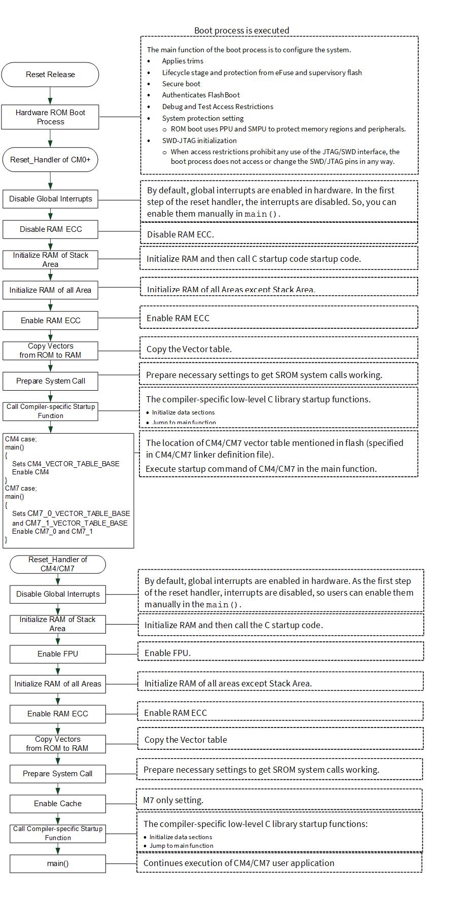
Startup flow example
The startup process is executed after the boot process completes. In the boot process, according to the lifecycle stage, protection status and debug access restriction setting are mainly performed, and application authentication is performed. In the startup process, initial settings necessary for program execution such as stack setting, RAM initialization, and clock settings are completed, and then execution jumps to the main routine. CM0+ executes the boot code after reset. CM4/CM7 will be activated after the boot process by the CM0+ user application.
Figure 7.
Device startup flow
Sample code
Code Listing 2 Sample code for CM0+ startup
;************************************************************************
;* Start-up Code
;************************************************************************
.weak Reset_Handler
.section ".text", "ax"
.thumb
Reset_Handler:
_start:
; Disable global interrupts
CPSID I
; Update Vector Table Offset Register with address of user ROM table
; (will be updated later to user RAM table address in C startup code)
LDR r0, =__vector_table
LDR r1, =VTOR
STR r0, [r1]
DSB
; CM0+ bus width is 32-bit, but SRAM is built with 64-bit based ECC on Traveo II parts with CM7 core
; Set CPUSS->RAMx_CTL0.ECC_CHECK_DIS bits to avoid causing unintentional ECC faults during startup while SRAM ECC has not been initialized yet
; Generic code can be used, even if RAMx_CTL0 (x > 0) registers are not implemented in a device
; or if no ECC_CHECK_DIS bits are available in the registers in case of m4cpuss with 32-bit ECC SRAM
MOVS r0, #1
LSLS r0, r0, #19
LDR r1, =CPUSS_RAM0_CTL0
LDR r2, [r1]
ORRS r2, r0
STR r2, [r1]
LDR r1, =CPUSS_RAM1_CTL0
LDR r2, [r1]
ORRS r2, r0
STR r2, [r1]
LDR r1, =CPUSS_RAM2_CTL0
LDR r2, [r1]
ORRS r2, r0
STR r2, [r1]
; Initialize ECC of startup stack (needed for local variables in C startup code) by processing 8 bytes per loop iteration,
; because the ECC initialization feature uses this generic granularity that will cover any memory (SRAM/TCM) in any TVII device
; Prerequisite: Stack Pointer (SP) has not been modified (from the vector table init value) by above code (otherwise code must be adapted)
MOVS r0, #0 ; clear value
MOVS r1, #0 ; clear value
LDR r2, Cy_u32StartupStackStartAddress
startup_stack_ecc_init_loop:
STM r2!, (r0, r1)
CMP r2, sp
BNE startup_stack_ecc_init_loop
; Call C startup code (no ANSI C context established yet!)
LDR r7, =Startup_Init
BLX r7
; Call system library
LDR r5, pool_myaddr
SUB r5, r5, 1 ; unset the low order bit
myaddr:
MOV r2, pc
SUB r5, r2, r5 ; Now r5 contains picbase
MOV r0, 0
MOV fp, r0 ;* No previous frame *
LDR r0, pool_baseptrs
ADD r0, r0, r5 ;* Add in picbase *
MOV r1, 0 ;* Clear argc reg *
MOV r2, 0 ;* Clear argv reg *
MOV r3, 0 ;* Clear envp reg *
MOV r4, 0 ;* Clear global regs *
MOV r5, 0
MOV r6, 0
LDR r7, =__ghs_ind_crt0
BLX r7
; Note: Control flow does not necessarily return here.
; On some tool-chains (e.g. IAR) control flow will never return from
; the system library.
Cy_Main_Exited:
B Cy_Main_Exited
.endf _start
Code Listing 3 Sample code for CM0+ main function
int main(void)
(
__enable_irq(); /* Enable global interrupts. /
/ Enable CM4. CY_CORTEX_M4_APPL_ADDR must be updated if CM4 memory layout is changed. */
Cy_SysEnableCM4(CY_CORTEX_M4_APPL_ADDR);
/* Place your initialization/startup code here (e.g. MyInst_Start()) */
Cy_GPIO_Pin_Init(USER_LED0_PORT, USER_LED0_PIN, &user_led0_port_pin_cfg);
for(;;)
(
DELAY(150000);
Cy_GPIO_Inv(USER_LED0_PORT, USER_LED0_PIN);
)
)
Code Listing 4 Sample code for CM4 startup
;************************************************************************
;* Start-up Code
;************************************************************************
.weak Reset_Handler
.section ".text", "ax"
.thumb2
Reset_Handler:
_start:
; Disable global interrupts
CPSID I
; Update Vector Table Offset Register with address of user ROM table
; (will be updated later to user RAM table address in C startup code)
LDR r0, =__vector_table
LDR r1, =VTOR
STR r0, [r1]
DSB
; Initialize ECC of startup stack (needed for local variables in C startup code) by processing 8 bytes per loop iteration,
; because the ECC initialization feature uses this generic granularity that will cover any memory (SRAM/TCM) in any TVII device
; Prerequisite: Stack Pointer (SP) has not been modified (from the vector table init value) by above code (otherwise code must be adapted)
MOVS r0, #0 ; clear value
MOVS r1, #0 ; clear value
LDR r2, Cy_u32StartupStackStartAddress
startup_stack_ecc_init_loop:
STRD r0, r1, [r2], #8
CMP r2, sp
BNE startup_stack_ecc_init_loop
; Call C startup code (no ANSI C context established yet!)
LDR r7, =Startup_Init
BLX r7
; Call system library
LDR r5, pool_myaddr
SUB r5, r5, 1 ; unset the low order bit
myaddr:
MOV r2, pc
SUB r5, r2, r5 ; Now r5 contains picbase
MOV r0, 0
MOV fp, r0 ;* No previous frame *
LDR r0, pool_baseptrs
ADD r0, r0, r5 ;* Add in picbase *
MOV r1, 0 ;* Clear argc reg *
MOV r2, 0 ;* Clear argv reg *
MOV r3, 0 ;* Clear envp reg *
MOV r4, 0 ;* Clear global regs *
MOV r5, 0
MOV r6, 0
LDR r7, =__ghs_ind_crt0
BLX r7
; Note: Control flow does not necessarily return here.
; On some tool-chains (e.g. IAR) control flow will never return from
; the system library.
Cy_Main_Exited:
B Cy_Main_Exited
.endf _start
Code Listing 5 Sample code for CM7 startup
;************************************************************************
;* Start-up Code
;************************************************************************
.weak Reset_Handler
.section ".text", "ax"
.thumb2
Reset_Handler:
_start:
; Disable global interrupts
CPSID I
; Update Vector Table Offset Register with address of user ROM table
; (will be updated later to user RAM table address in C startup code)
LDR r0, =__vector_table
LDR r1, =VTOR
STR r0, [r1]
DSB
; Allow write access to Vector Table Offset Register and ITCM/DTCM configuration register (CPUSS_CM7_X_CTL.PPB_LOCK[3] and CPUSS_CM7_X_CTL.PPB_LOCK[1:0])
LDR r1, =CPUSS_IDENTITY ; first check master identity (CM7_0 or CM7_1?)
LDR r0, [r1]
LSR r0, r0, #8
AND r0, r0, #0xf
CMP r0, #MASTER_ID_CM7_0
ITE EQ ; load address of corresponding CPUSS_CM7_x_CTL register
LDREQ r1, =CPUSS_CM7_0_CTL
LDRNE r1, =CPUSS_CM7_1_CTL
LDR r0, [r1]
BIC r0, r0, #0xb
STR r0, [r1]
DSB
; Enable ITCM and DTCM
LDR r1, =ITCMCR
LDR r0, [r1]
ORR r0, r0, #0x7 ; Set ITCMCR.EN, .RMW and .RETEN fields
STR r0, [r1]
LDR r1, =DTCMCR
LDR r0, [r1]
ORR r0, r0, #0x7 ; Set DTCMCR.EN, .RMW and .RETEN fields
STR r0, [r1]
DSB
ISB
; Initialize ECC of startup stack (needed for local variables in C startup code) by processing 8 bytes per loop iteration,
; because the ECC initialization feature uses this generic granularity that will cover any memory (SRAM/TCM) in any TVII device
; Prerequisite: Stack Pointer (SP) has not been modified (from the vector table init value) by above code (otherwise code must be adapted)
MOVS r0, #0 ; clear value
MOVS r1, #0 ; clear value
LDR r2, Cy_u32StartupStackStartAddress
startup_stack_ecc_init_loop:
STRD r0, r1, [r2], #8
CMP r2, sp
BNE startup_stack_ecc_init_loop
; Call C startup code (no ANSI C context established yet!)
LDR r7, =Startup_Init
BLX r7
; Call system library
LDR r5, pool_myaddr
SUB r5, r5, 1 ; unset the low order bit
myaddr:
MOV r2, pc
SUB r5, r2, r5 ; Now r5 contains picbase
MOV r0, 0
MOV fp, r0 ;* No previous frame *
LDR r0, pool_baseptrs
ADD r0, r0, r5 ;* Add in picbase *
MOV r1, 0 ;* Clear argc reg *
MOV r2, 0 ;* Clear argv reg *
MOV r3, 0 ;* Clear envp reg *
MOV r4, 0 ;* Clear global regs *
MOV r5, 0
MOV r6, 0
LDR r7, =__ghs_ind_crt0
BLX r7
; Note: Control flow does not necessarily return here.
; On some tool-chains (e.g. IAR) control flow will never return from
; the system library.
Cy_Main_Exited:
B Cy_Main_Exited
.endf _start
Peripheral drivers
Peripheral drivers are a set of firmware drivers that provide APIs for accessing hardware. These APIs perform initialization and control activities of each peripheral.
Peripheral drivers list
Table 4 lists the peripheral drivers that Infineon provides for SDL.
No. | Module | Description | TRAVEO™ T2G family | ||
|---|---|---|---|---|---|
CYT2B | CYT3B/4B/6B | CYT4D | |||
1 | ADC | Analog-to-digital converter | ✓ | ✓ | ✓ |
2 | Audioss | Sound subsystem for I2S, DAC, mixer, PWM, SG, TDM | – | – | ✓ |
3 | AXIDMA | M-DMA on AXI bus | – | – | ✓ |
4 | CANFD | CAN FD | ✓ | ✓ | ✓ |
5 | CPU | Enables core of CPU-specific features | ✓ | ✓ | ✓ |
6 | CRYPTO | Cryptography | ✓ | ✓ | ✓ |
7 | CXPI | Manages communication over the CXPI interface | ✓ | – | ✓ |
8 | DMA | M-DMA, P-DMA | ✓ | ✓ | ✓ |
9 | ETHERNET | Basic Ethernet driver supporting automotive and Gigabit Ethernet PHY | – | ✓ | ✓ |
10 | EVTGEN | Event generator | ✓ | ✓ | ✓ |
11 | FLASH | Code Flash, Work Flash | ✓ | ✓ | ✓ |
12 | FLEXRAY | Manages FlexRay communication | – | ✓ | – |
13 | FPDLINK | FPD-link or LVDS | – | – | ✓ |
14 | GPIO | GPIO | ✓ | ✓ | ✓ |
15 | GFX_ENV | Graphics environment setup | – | – | ✓ |
16 | I2S | Manage inter-IC sound. I2S is used to send digital audio streaming data to external I2S devices, such as audio codecs or simple DACs. It can also receive digital audio streaming data. | – | ✓ | – |
17 | IPC | Inter-processor communication | ✓ | ✓ | ✓ |
18 | LIN | Local interconnect network | ✓ | ✓ | ✓ |
19 | LVD | Provides LVD capabilities | ✓ | ✓ | ✓ |
20 | MCWDT | Multi-counter watchdog timers | ✓ | ✓ | ✓ |
21 | MIPICSI2 | Video input | – | – | ✓ |
22 | MPU | Memory protection unit | ✓ | ✓ | ✓ |
23 | PROT | Protection unit | ✓ | ✓ | ✓ |
24 | SCB | Serial communication block (SCB) - EZI2C, SCB - I2C, SCB - SPI, SCB - UART | ✓ | v | ✓ |
25 | SD_HOST | Manages SD and eMMC devices | – | ✓ | – |
26 | SMART IO | Configure and access the Smart I/O hardware present between the GPIOs (pins) and HSIOMs (pin muxes) on select device ports. It can be used to perform simple logic operations on peripheral and GPIO signals at the GPIO port. | ✓ | ✓ | ✓ |
27 | SMIF | SPI-based communication interface for interfacing external memory devices to TRAVEO™ T2G. The SMIF supports octal-SPI, dual quad-SPI, quad-SPI, DSPI, and SPI. This interface also supports HYPERBUS™ interfaces like HYPERRAM™ and HYPERFLASH™ devices. | – | ✓ | ✓ |
28 | SROM | Internal SROM driver | ✓ | ✓ | ✓ |
29 | SYSCLK | System clock | – | ✓ | ✓ |
30 | SYSFLT | System fault | ✓ | ✓ | ✓ |
31 | SYSINT | System interrupt | ✓ | ✓ | ✓ |
32 | SYSLIB | System library | ✓ | ✓ | ✓ |
33 | SYSPM | System power management | ✓ | ✓ | ✓ |
34 | SYSREGHC/SYSPMIC | REGHC/PMIC control and status | – | ✓ | – |
35 | SYSRESET | Provides APIs for reading reset reason and clearing them | ✓ | ✓ | ✓ |
36 | SYSRTC | System real-time clock | ✓ | ✓ | ✓ |
37 | SYSTICK | SysTick timer | ✓ | ✓ | ✓ |
38 | SYSWDT | Free running watchdog timer | ✓ | ✓ | ✓ |
39 | TCPWM | Timer counter PWM | ✓ | ✓ | �✓ |
40 | TRIGMUX | Trigger multiplexer | ✓ | ✓ | ✓ |
Example usage of SDL with GHS MULTI
Environment for SDL
This section describes the operation with CYT2B7 series SDL as an example.
SDL operational conditions:
CPU: CYT2B7 series
Target board: TRAVEO™ T2G evaluation board
IDE: GHS MULTI V7.1.4 (compiler version 2017.1.4)
Used API module GPIO
Install GHS MULTI and SDL
Install GHS MULTI, set license, and set probe firmware in advance.
Install SDL according to SDL’s instructions in advance.
Setup debug script and configuration files
Using the scripts tvii_detect.py and multi.irc , in C:...\TVII_Sample_Driver_Library_revision\misc\tools\ghs\debugging\AppData_GHS , you can execute the run process.
The process includes configuring probe, connecting target, and downloading the program into RAM. You will also be able to use detect the debugger script (D) button and load the program to the RAM (R) button.
Copy the files, tvii_detect.py and multi.irc to the <%APPDATA%\GHS> folder (that is, C:\Users<LOGIN_NAME>\AppData\Roaming\GHS) on the PC.
If you are unable to find the AppData folder, follow these steps to display the hidden folders:
In Windows Explorer, go to the View tab.
Click Options .
In the folder options dialog, go to the View tab.
Select show hidden files, folders, and drives.
Click OK .
Setup with MULTI
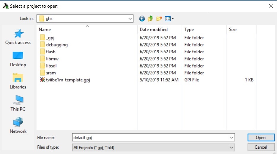
Start the MULTI project manager and open the SDL project file:
C: \…\TVII_Sample_Driver_Library_revision\tools\ghs\tviibe1m_template.gpj
Figure 8.
Select the SDL project
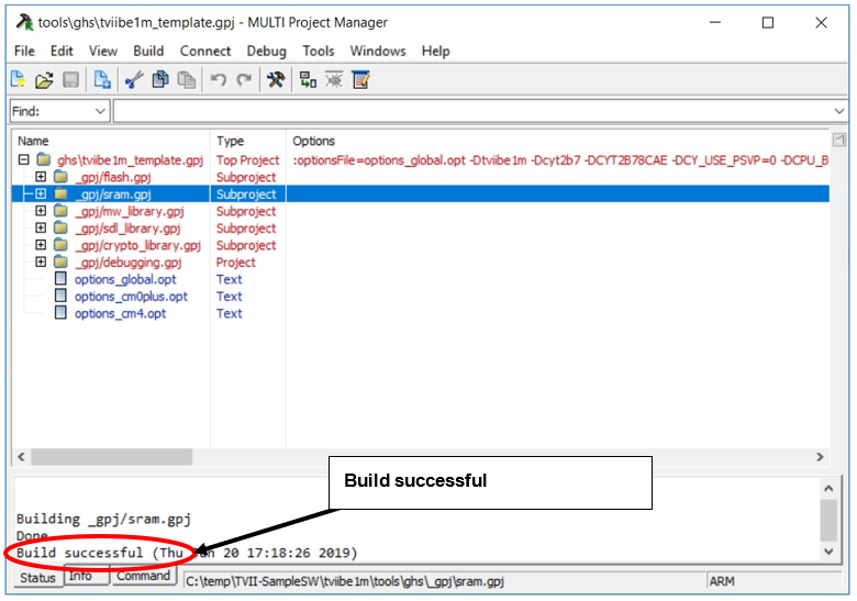
For the build, select sram.gpj and click the hammer icon as shown in Figure 9 . The build starts and successful messages appear as shown in Figure 10 .
Figure 9.
Build the project of SDL project
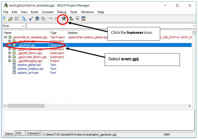
Figure 10.
Build successful of the project of SDL project
There are two debugging methods:
Debugging with download on the RAM
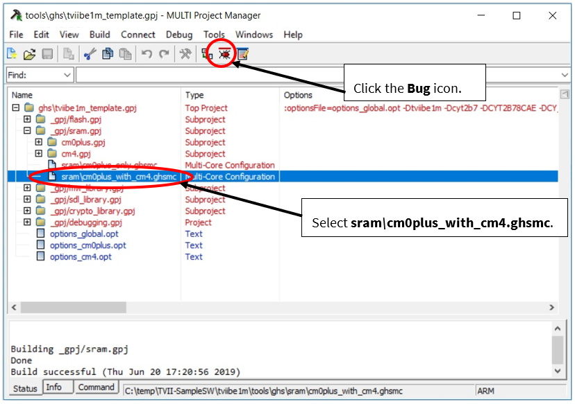
For execution on the RAM, select sram\cm0plus_with_cm4.ghsmc and click the Bug icon as shown in Figure 11 . Debugging of the program on the RAM begins.
Figure 11.
Debug the project of SDL project
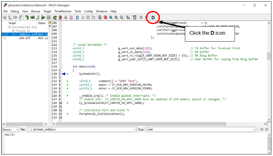
To enable the SDL project to detect the debugger script, click the D icon as shown in Figure 12 .
Figure 12. Debug the project of SDL project
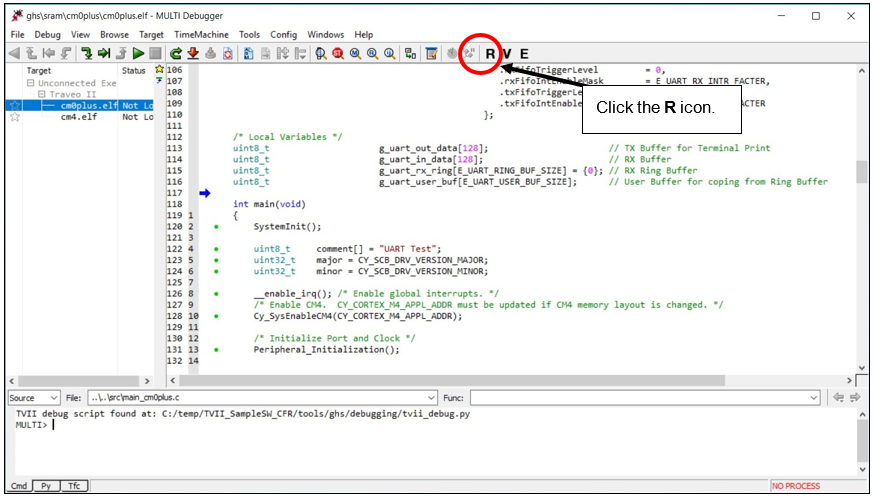
To load the program to the RAM, click the R icon as shown in Figure 13 . Loading of the program to the RAM begins.
Figure 13.
Load to RAM
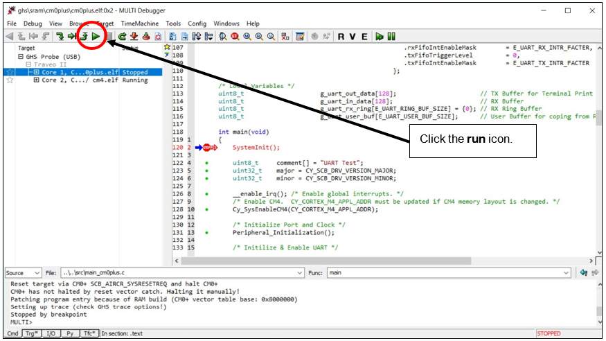
Click the run icon as shown in Figure 14 .
Figure 14.
Execution on RAM
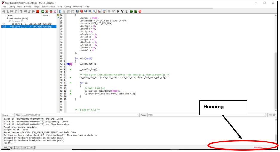
When these operations are performed, both CM0+ and CM4 programs will be in the program running state as shown in Figure 15 and debugging will be possible. The board LED starts blinking.
Figure 15. Running on the RAM
Debugging with download on the Flash memory
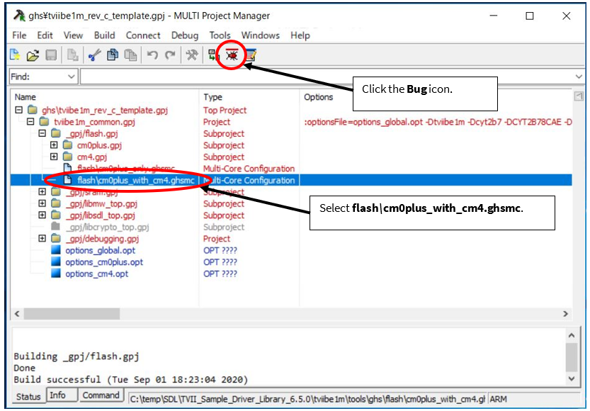
For execution on the Flash memory, select flash\cm0plus_with_cm4.ghsmc and click the Bug icon as shown in Figure 16 . Debugging of the program on the Flash memory begins.
Figure 16.
Debug the project of SDL project
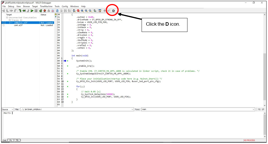
To enable the SDL project to detect the debugger script, click the D icon as shown in Figure 17 .
Figure 17.
Debug the project of SDL project
To load the program to the Flash memory, click the F icon as shown in Figure 18 . Loading of the program to the Flash memory begins.
Figure 18.
Load to Flash memory

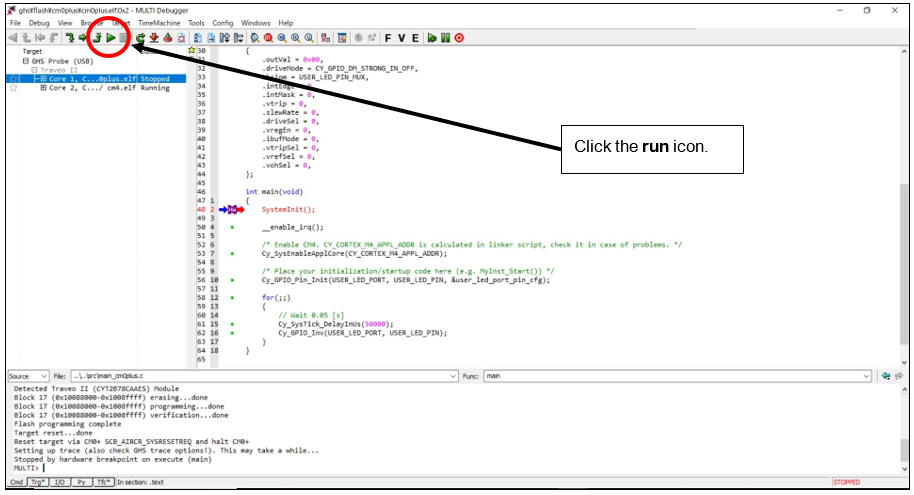
Click the run icon as shown in Figure 19 .
Figure 19.
Execution on Flash memory
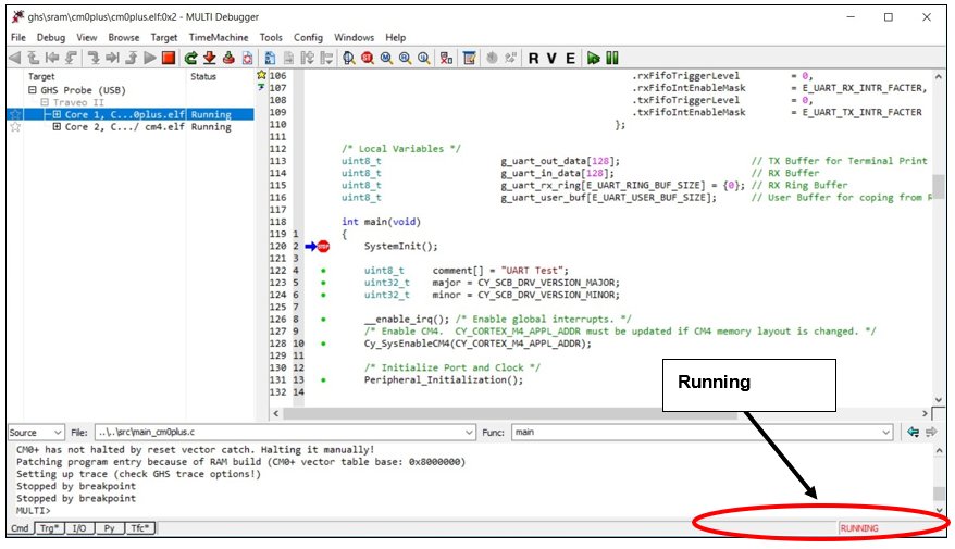
When these operations are performed, both CM0+ and CM4 programs will be in the program running state and debugging will be possible. The board LED starts blinking.
Figure 20.
Running on the Flash memory
Example usage of SDL with IAR embedded workbench for Arm®
Environment for SDL
This section describes the operation with CYT2B7 series SDL as an example.
SDL operational conditions:
CPU: CYT2B7 series
Target board: TRAVEO™ T2G evaluation board
IDE: IAR Embedded Workbench for Arm® (compiler version 8.42.1)
Used API module GPIO
Install GHS MULTI and SDL
Install IAR Embedded Workbench for Arm®, set the license, and I-Jet in advance.
Install SDL according to SDL's instructions in advance.
Setup with IAR EWARM
There are two debugging methods:
Debugging with download on the RAM
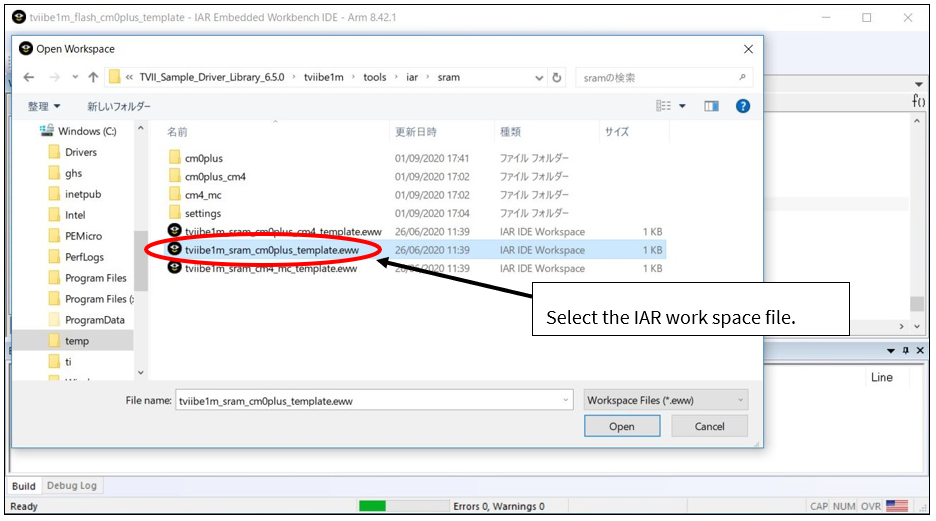
Start IAR EW for Arm® and open the SDL work space file:C: \…\TVII_Sample_Driver_Library_revision\tviibe1m\tools\iar\sram\tviibe1m_sram_cm0plus_template.eww
Figure 21.
Select the SDL workspace
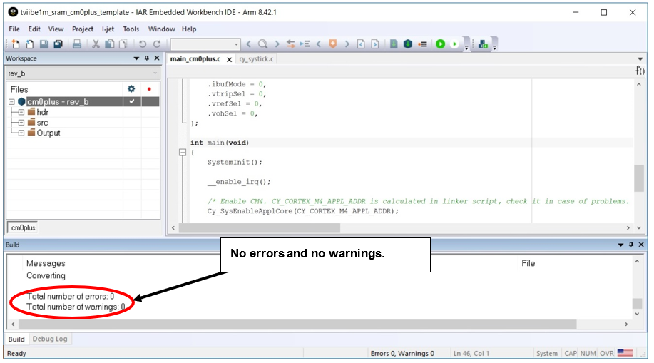
For the build, select cm0plus.eww on the workspace and right-click and select Rebuild All as shown in Figure 22 . The Rebuild All process starts, and no errors and no warnings messages appear as shown in Figure 23 .
Figure 22.
Rebuild the project of SDL project
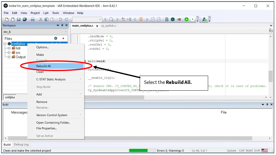
Figure 23.
Rebuild successful of the project of SDL project
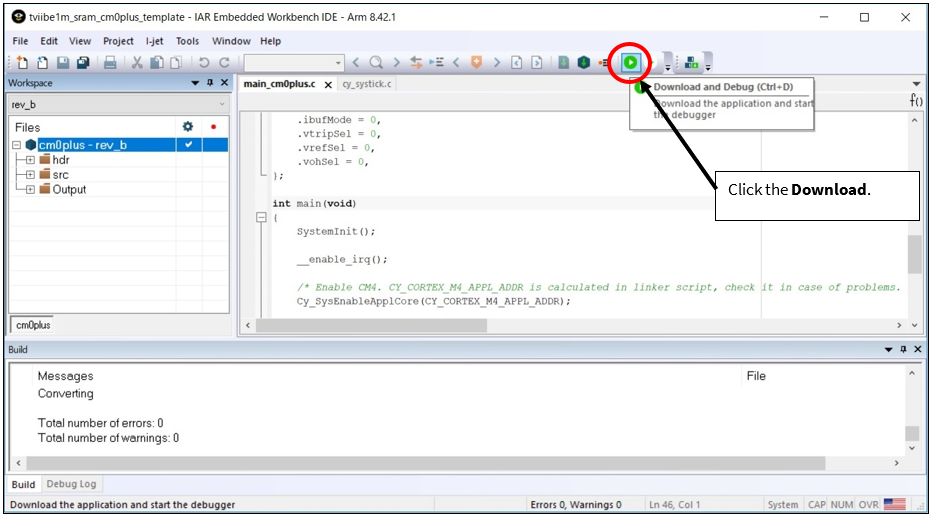
To load the program to the RAM, click the Download icon as shown in Figure 24 .
Figure 24.
Debug the project of SDL project
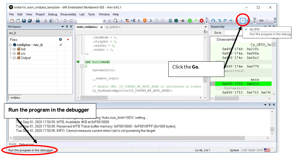
Click the Go icon as shown in Figure 25 .
Figure 25.
Execution on RAM
When these operations are performed, both CM0+ programs will be in the program running state and debugging will be possible as shown in Figure 29 . The board LED starts blinking.
Debugging with download on the Flash memory
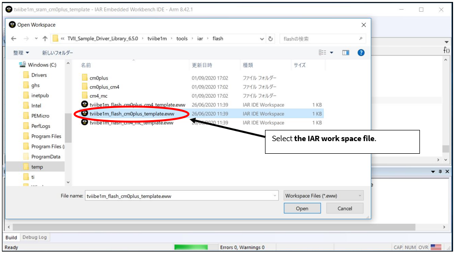
Start the IAR EW for Arm® and open the SDL work space file:
C:\…\TVII_Sample_Driver_Library_revision\tviibe1m\tools\iar\flash\tviibe1m_flash_cm0plus_template.eww
Figure 26.
Select the SDL workspace
For the build, select cm0plus.eww on the workspace and right-click and select Rebuild All as shown in Figure 27 . The Rebuild All process starts, and no errors and no warnings messages appear as shown in Figure 28 .
Figure 27.
Rebuild the project of SDL project
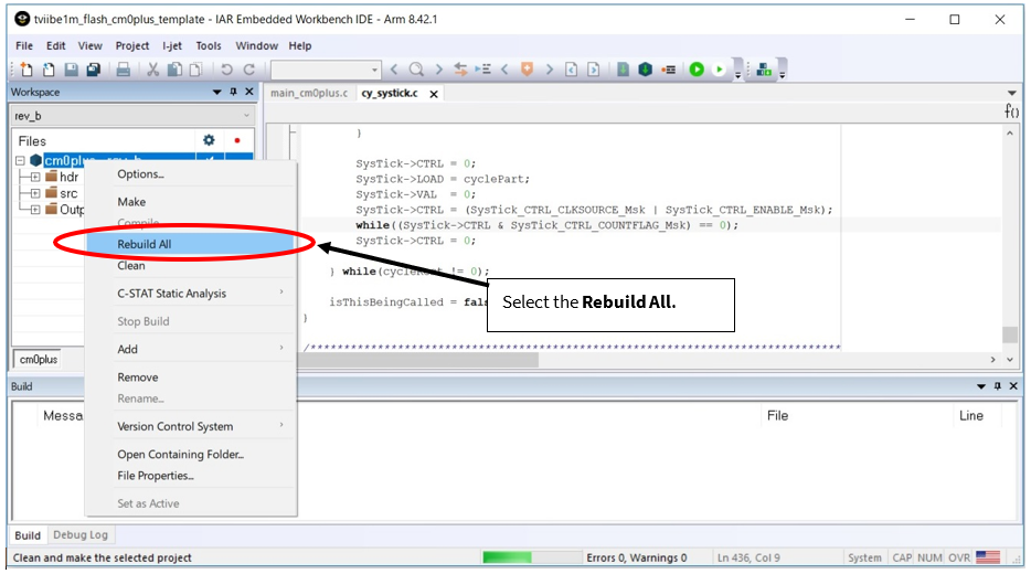
Figure 28.
Rebuild successful of the project of SDL project
To load the program to the Flash memory, click the Download icon as shown in Figure 29 .
Figure 29.
Debug the project of SDL project
Click the Go icon as shown in Figure 30 .
Figure 30.
Execution on Flash memory
When these operations are performed, both CM0+ programs will be in the program running state and debugging will be possible as shown in Figure 30 . The board LED starts blinking.
Development tools
Table 5 lists the details of support development tools.
Vender | Emulators/probes | Compiler |
|---|---|---|
Green Hills Software Ltd. | GHS probe (5.6.4/5.6.6) | MULTI V7 (version 7.1.4) |
IAR Systems AB | I -JET | Embedded Workbench for Arm® (8.42.1) |
iSYSTEM AG | i-TAG family | – |
Lauterbach GmbH | TRACE 32-ICE | – |
Flash programming tools
Table 6 lists the supported flash programming tools. Infineon MiniProg3/4 programmer is for development purposes. For mass production purposes, JTAG programmer from a third-party is suitable.
Vender | Flash programmer | Software | Notes |
|---|---|---|---|
Infineon Technologies AG | Miniprog3 | Infineon Programmer 1.0 | Support only for CYT2B7 |
Miniprog4 | Infineon Auto Flash Utility | ||
SEGGER Microcontroller GmbH | J-Link | J-Flash | |
Flasher Arm® (for mass production) | |||
DTS Insight Corp. | NETIMPRESS AF430 | Remote Controller AZ490 |
CYTVII-B-E-1M-xxx-CPU/CYTVII-B-H-8M-xxx-CPU/CYTVII-C-2D-6M-xxx-CPU has the Cortex® debug connector for both functions JTAG and SWD. SWD compatible with MiniProg3.
Table 7 lists the pin assignment for Cortex® debug connector.
Pin | Signal |
|---|---|
1 | VCC |
2 | SWDIO/TMS |
3 | GND |
4 | SWDCLK/TCK |
5 | GND |
6 | SWO/TDO |
7 | KEY |
8 | NC/TDI |
9 | GNDDetect |
10 | nRESET |
Summary
This application note guided you to set up TRAVEO™ T2G development environment. Infineon provides a wealth of evaluation boards and sample software to help you get started with TRAVEO™ T2G family. To evaluate the CYT2/CYT3/CYT4 series evaluation boards, contact your sales representative or Infineon Technical Support .
Glossary
Terms | Description |
|---|---|
ADC | analog-to-digital converter |
ASIL-B | automotive safety integrity level-B |
CAN FD | Controller Area Network with Flexible Data rate |
CMSIS | Cortex® microcontroller software interface standard |
Crypto | cryptography accelerator |
CXPI | clock extension peripheral interface |
DMA | direct memory access |
ETM | Embedded Trace Macrocell |
EVTGEN | event generator |
FDP-Link | flat panel display link |
Gigabit Ethernet | 1 Gbps Ethernet |
GPIO | general-purpose input/output |
IPC | inter-processor communication |
JTAG | joint test action group |
LIN | Local Interconnect Network |
MCWDT | multi-counter watchdog timers |
MPU | memory protection unit |
LVDS | low voltage differential signaling |
MIPI | mobile industry processor interface |
CSI2 | camera serial interface-2 |
PROT | protection unit |
RWW | read-while-write |
SCB | serial communication block |
SDL | Sample Driver Library |
SWD | single wire debug |
SYSCLK | system clock |
SYSFLT | system fault |
SYSINT | system interrupt |
SYSLIB | system library |
SYSPM | system power management |
REGHC | high current regulator |
SYSRTC | system real-time clock |
SYSTICK | systick timer |
SYSWDT | free running watchdog timer |
TCPWM | timer counter PWM |
TRIGMUX | trigger multiplexer |
Related documents
The following are the TRAVEO™ T2G family series application notes, datasheets and technical reference manuals. Contact Technical Support to obtain these documents.
Documents | Description |
|---|---|
Application notes | |
Describes how to set up a hardware environment for TRAVEO™ T2G. | |
Device datasheet | |
CYT2B7 datasheet 32-bit Arm®
Cortex®-M4F microcontroller TRAVEO™ T2G family | Describes the functions and electrical specifications of the target product. It also includes product specific information such as address map, I/O map, pin assignment, alternate function pin assignments, interrupt source list, trigger group, peripheral clocks, faults, bus masters |
CYT2B9 datasheet 32-bit Arm® Cortex®-M4F
microcontroller TRAVEO™ T2G family | |
CYT4BF datasheet 32-bit Arm® Cortex®-M7
microcontroller TRAVEO™ T2G family | |
CYT4DN datasheet 32-bit Arm® Cortex®-M7 microcontroller TRAVEO™ T2G family (Doc No. 002-24601) | |
CYT3BB/4BB datasheet 32-bit Arm® Cortex®-M7 microcontroller TRAVEO™ T2G family | |
CYT3DL datasheet 32-bit Arm® Cortex®-M7 microcontroller TRAVEO™ T2G family (Doc No. 002-27763) | |
CYT6BJ datasheet 32-bit Arm® Cortex® -M7 microcontroller TRAVEO™ T2G family (Doc No. 002-33466) | |
Architecture technical reference manual | |
TRAVEO™ T2G automotive body controller
entry family architecture technical reference manual (TRM) | Describes the architecture and functioning of product family |
TRAVEO™ T2G automotive body controller
high family architecture technical reference manual (TRM) | |
TRAVEO™ T2G automotive cluster 2D family architecture technical reference manual (TRM) (Doc No. 002-25800) | |
Registers technical reference manual | |
TRAVEO™ T2G automotive body controller
entry registers technical reference manual (TRM) for CYT2B7 | Describes the registers list, the initial values, and attributes of the registers of product family |
TRAVEO™ T2G automotive body controller
entry registers technical reference manual (TRM) for CYT2B9 | |
TRAVEO™ T2G automotive body controller
high registers technical reference manual (TRM) for CYT4BF | |
TRAVEO™ T2G automotive cluster 2D registers technical reference manual (TRM) for CYT4DN (Doc No. 002-25923) | |
TRAVEO™ T2G automotive cluster 2D registers technical reference manual (TRM) for CYT3DL (Doc No. 002-29854) | |
TRAVEO™ T2G automotive body controller high registers technical reference manual (TRM) for CYT6BJ (Doc No. 002-36068) | |
Revision history
Document version | Date of release | Description of changes |
|---|---|---|
** | 2017-12-26 | New application note. |
*A | 2019-01-24 | Updated Associated Part Family as “TRAVEO™ T2G Family CYT2B/CYT4B Series”. Added target part numbers “CYT2B9 Series” and “CYT4BF Series” related information in all instances across the document. |
*B | 2019-05-07 | Updated Associated Part Family as “TRAVEO™ T2G Family CYT2B/CYT4B/CYT4D Series”. Added target part numbers “CYT4D Series” related information in all instances across the document. Updated Feature Set: Added “CYT4D Series”. Updated Development Environment and Tools: Updated Peripheral Drivers: Updated Peripheral Drivers List: Updated “Table 4. Peripheral Drivers List”. Updated Example Usage of SDL with GHS MULTI: Added “Install GHS MULTI and SDL”. Added “Setup debug script and configuration files”. Updated Flash Programming Tools: Updated “Table 6. Flash Programming Tools”. Updated Glossary. Updated Related Documents. |
*C | 2020-03-24 | Updated Associated Part Family as “TRAVEO™ T2G Family CYT2/CYT3/CYT4 Series”. Changed target part numbers from “CYT2B/CYT4B/CYT4D Series” to “CYT2/CYT4 Series” in all instances across the document. Added target part numbers “CYT3 Series” in all instances across the document. |
*D | 2020-09-14 | Updated Development Environment and Tools: Updated Example Usage of SDL with GHS MULTI: Updated Setup with MULTI: Updated almost entire section. Added “Example Usage of SDL with IAR Embedded Workbench for Arm”. |
*E | 2021-03-29 | Added Summary. Updated to Infineon template. |
*F | 2021-11-12 | Added Note on CPU (CM0+ and CM4) startup sequence for CYT2B series and CPU (CM0+ and CM7) startup sequence for CYT4B/CYT4D series . |
*G | 2023-11-09 | Template update; no content change |
*H | 2024-03-28 | Added section CYT6B series |