Drawing schematic symbols
Automatic symbol creation
You can automatically generate the schematic symbol of the IGBT while creating its project-local component, on condition that the IGBT_1200V_TRENCHSTOP_IGBT7_CS7_L1 model library file is present in the 'Tutorial' project.
- Right-click the 'Tutorial' project and choose New Local Component in the upcoming menu
- Enter 'IGBT' as component name in the upcoming dialog


Alternatively, you can use the menu:
- or select the icon
 of the
Workspace toolbar
of the
Workspace toolbar
Another dialog then appears with various settings for the new project-local component.
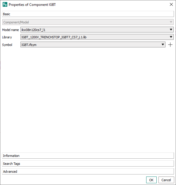
The upcoming dialog consists of four tabs: Basic, Information, Search Tags and Advanced.
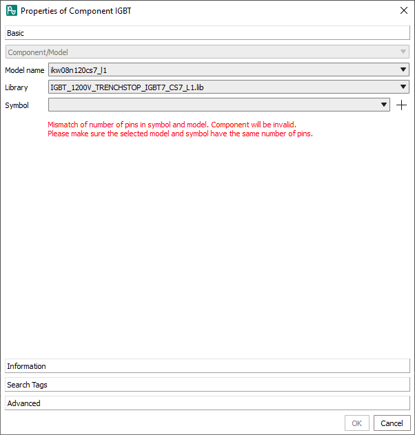
The Basic tab is used specify the library file, the
symbol and the default model of the new component. The settings Model name, and Library are thereby already filled in. The drop-down menu of the
Model name setting contains all
available device types extracted from library file and can be freely chosen. Here,
it will be left at its default value
ikw08n120cs7_l1.
The Symbol is still missing and will be generated in the following:
- Click on the button +
- Enter 'IGBT' as symbol name in the upcoming dialog

The pin positions of the symbol must then be specified as follows:
- Left Pins: 'G'
- Top Pins: 'C'
- Bottom Pins: 'E'
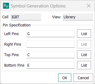
After pressing OK, the symbol is created. After also pressing OK in the New Local Component dialog, the new project-local component 'IGBT' appears in the 'Tutorial' project.
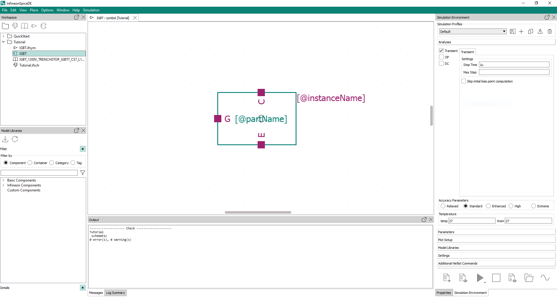
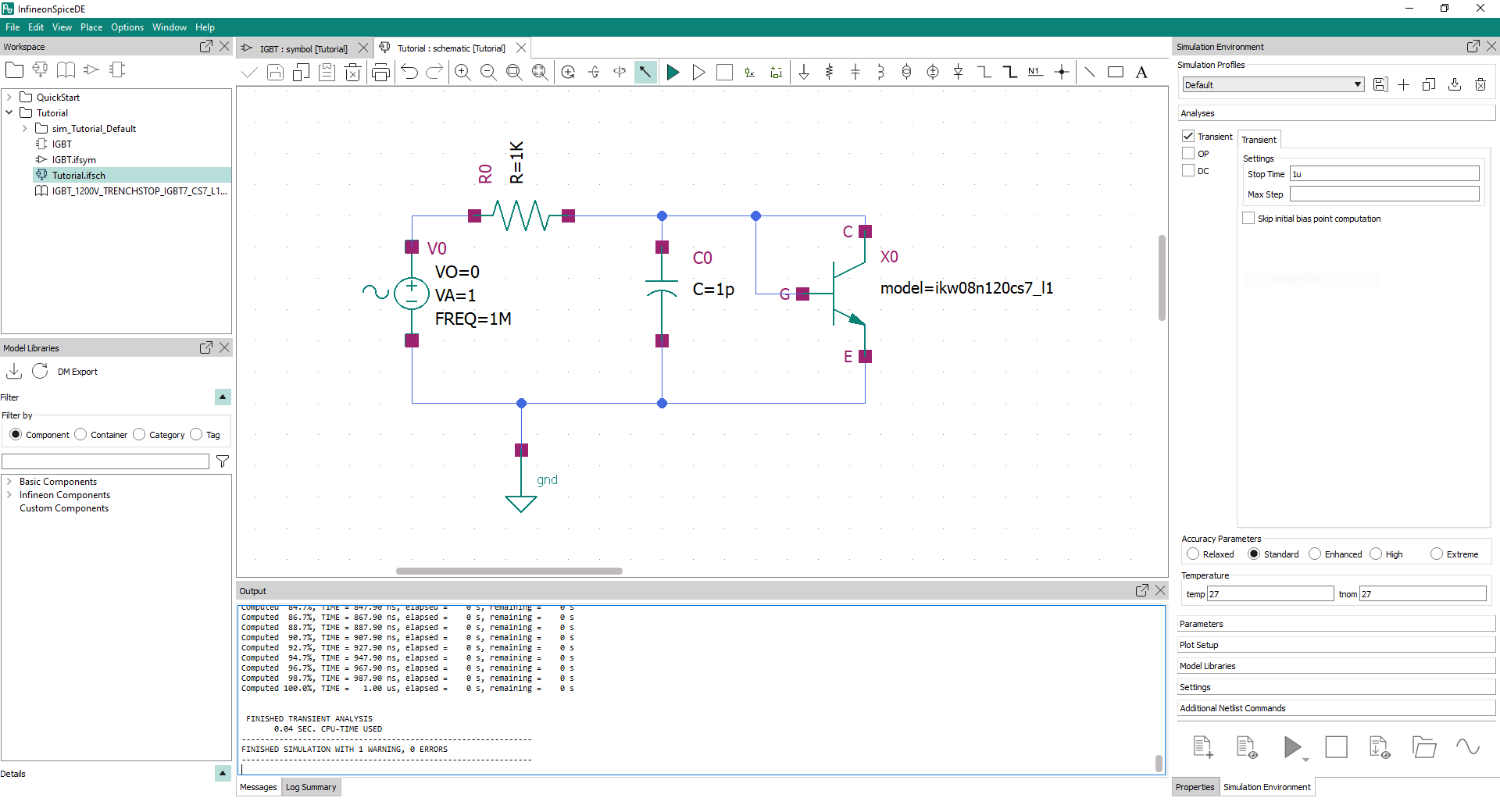
You can now drag and drop this component into the 'Tutorial' schematic and simulate it.
To inspect the properties of the newly created component, right-click on it in the Workspace and select Open Properties....
The Information tab can be used to add a Description, Version, ISPN or URLs to the product or documentation of the component.
In the Search Tags tab, keywords used by the filters of the Model Libraries window can be specified.
The Advanced tab allows to specify pin mappings between the symbol and the sub-circuit definition of the library file of the component and also to set default values for its model parameters. These settings are then used by the netlister to print occurrences of the component in a schematic correctly into the corresponding simulatable netlist. If no advanced settings are provided, default netlisting routines are used which are sufficient for most applications.
Manual symbol creation
To create a new symbol manually:
- Right-click on the 'Tutorial' project
- Choose New Symbol...

- Enter a name, for example 'IGBT', and click on OK
In the symbol editor, the menu Place or its toolbar can be used to place pins and draw shapes to create a graphical representation of the new component.

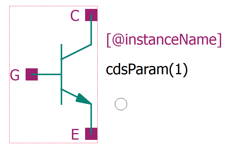
IGBTs are typically visualized in schematics by the following symbol.

Drawing symbols in the symbol editor
This sections shows how to draw symbol in the symbol editor.
First, the pins of the device are placed into the empty symbol view.
- Press P or click on the following icon in
the toolbar:

- Enter the pin name, the pin direction and the pin type in the following dialog
For consistency, the pin names should correspond to the pin names in the sub-circuit definition of the model file (here 'C', 'G' and 'E'). If the pin names should be hidden in the schematic, untick the checkbox Visible in the pin attributes dialog

The pin direction indicates whether the pin is an input or an output of the device. If the pin can be used in both directions, select inputOutput (default). The chosen pin direction does not affect the simulation, but might be important for other tools and should be correctly set. The attribute Type determines the shape of the pin and can be either round or square.

The sub-circuit definition of the IGBT has three pins, that is, C, G and E. These three pins have to be present in the new symbol.
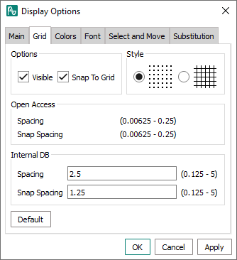
After placing the pins, you can draw the device symbol using the line or arrow symbol from the toolbar. To adjust the spacing of the symbol editor, use the settings 'Spacing' and 'Snap Spacing' under the menu . Smaller spacing allows a fine grained control over the placement of the symbol's shapes. The spacing can be reset by clicking on the button Default in the same dialog.
You can automatically generate the bounding box of the symbol by clicking the
right-most icon in the toolbar and choose 'Automatic' in the upcoming dialog, .
.


Finally, you can place text macros into the symbol that specify which
properties of the device should be displayed in the schematic. To define these so
called 'substitution field attributes', click on the icon  .
.
A dialog opens in which you can define the display name and device parameters.


- 'instance label'/
[@instanceName]: Create a device name label in the schematic - 'analog device annotate'/
cdsParam(x): Displaying parameter 'x' of the device in the schematic, with 'x' being a positive integer number
Afterwards you can create the project-local component for the IGBT by right-clicking the 'Tutorial' project.
- Right-click the 'Tutorial' project
- Select New Local Component from the upcoming menu
- Enter 'IGBT' in the upcoming dialog
The next dialog has all necessary settings for the new local component already filled in, which can then be created by clicking on OK.
You can now place The created component into the 'Tutorial' schematic and simulate it.