AN0006 Analog system block in PSOC™ HV MS family
About this document
Scope and purpose
This application note introduces you to the analog system block of PSOC™ HV mixed signal (MS) family MCUs. This application note also guides you to develop hardware and firmware design for human-machine interface (HMI), body, and powertrain applications.
Intended audience
This document is intended for hardware and firmware design engineers.
Introduction
PSOC™ HV MS is a fully-integrated programmable embedded system for several automotive HMI, body, and powertrain applications. The system features an Arm® Cortex® M0+ processor with programmable and reconfigurable analog and digital blocks. It is a combination of a microcontroller with a 12-bit SAR ADC, 5
th
-generation multi-sense converter (MSC) block supporting capacitive sensing (CAPSENSE™), digital peripherals such as PWMs and serial communication interfaces along with a LIN interface with integrated PHY, and a high-voltage subsystem to operate directly off the 12-V car battery.
PSOC™ HV MS is available in a 32-/48-/56-/64-QFN package with wettable flanks. To get a better understanding of the functionality described and terminology used in this application note, it is a good idea to read the “Section A: Overview” chapter of the architecture technical reference manual (architecture TRM) and AN85951 - PSOC™ 4 and PSOC™ 6 MCU CAPSENSE™ design guide. For more details, see References.
Analog system overview
The analog system (see
Figure 1
) in PSOC™ HV MS includes a successive approximation register analog-to-digital converter (SAR ADC), low-power comparator (LPCOMP), continuous-time block mini (CTBm), and CAPSENSE™ block.
Note: This document does not describe the CAPSENSE™ block in detail. For more details, see AN0005 - CAPSENSE™ (multi-sense converter) block in PSOC™ HV MS family in References.
Figure 1. Analog system block diagram
SAR ADC
PSOC™ HV MS has a SAR ADC, which is designed for applications that require moderate resolution and high data rate. It consists of the following blocks (see
Figure 2
):
Figure 2. SAR ADC block diagram
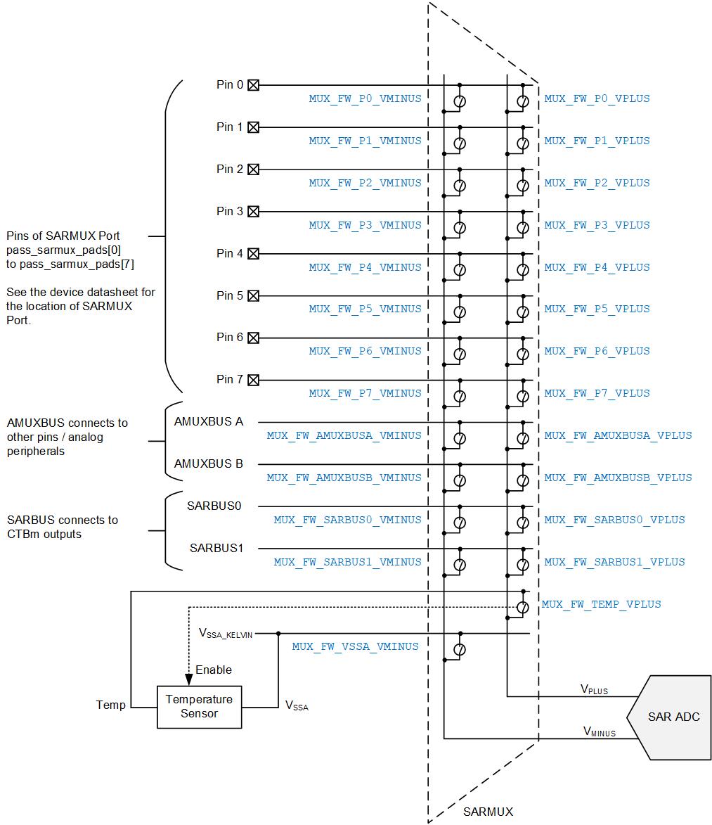
Before the SAR ADC, there are three multiplexers to route to the 16 internal channels (MS-64K) or 24 internal channels (MS-128K) of the SAR ADC. The DIAGMUX/ EXPMUX also has broken wire detection to check for broken wires from IO to the ADC.
SARMUX: Routes external pins and internal signals (AMUXBUS-A/-B, CTBm, temperature sensor output)
DIAGMUX: Configurable to measure various supply voltages, reference voltages and grounds on-chip
EXPMUX (for MS-128K): Expansion analog inputs from 8x GPIO
SAR ADC core: Fast 12-bit ADC with 1 Msps sampling rate
SARREF: Used for multiple reference selection
SARSEQ: The sequencer controller (SARSEQ) is used to control SARMUX, DIAGMUX, EXPMUX and SAR ADC to do an automatic scan on all enabled channels without CPU intervention and for pre-processing, such as averaging the output data
The result from each channel is double-buffered; a complete scan may be configured to generate an interrupt at the end of the scan. The sequencer may also be configured to flag overflow, collision, and saturation errors that can be configured to assert an interrupt.
For more flexibility, it is also possible to control most analog switches, including those in SARMUX/DIAGMUX/EXPMUX with the firmware. This makes it possible to implement an alternative sequencer with the firmware.
The SAR ADC block provides the following features:
Operates across the entire device power supply range
Sample rate up to 1 Msps
16x(MS-64K)/24x (MS-128K) individually configurable channels that can scan various input sources and one injection channel
Each channel has the following features:
Input from an external pin (only for eight channels in single-ended mode and four channels in differential mode) or internal signal (AMUXBUS/CTBm/temperature sensor/diagnostic inputs)
Programmable acquisition times
Selectable 8-, 10-, and 12-bit resolution
Single-ended or differential measurement
Averaging
Results are double-buffered
Result may be left- or right-aligned
Diagnostic current sources and sinks (DIAG current SRC/SINK) to check for broken wires
Scan triggered by firmware, timer, low-power comparator, and by the SAR end-of-conversion signal
Hardware/firmware trigger (one-shot), and free-running (continuous conversion) modes
Hardware averaging support
First-order accumulate
Samples averaging from 2 to 256 (powers of 2)
Results represented in 16-bit sign-extended values
Selectable voltage references
Internal VDDA and VDDA/2 references
Internal 1.2 V reference with buffer
External reference
Interrupt generation
Finished scan conversion
Saturation detection and over-range (configurable) detection for every channel
Scan results overflow
Collision detection
Configurable injection channel
Triggered by firmware
Can be interleaved between two scan sequences (tailgating)
Selectable sample time, resolution, single-ended, or differential averaging
Low-power modes
ADC core and reference voltage have dedicated low-power modes
Internal AHB bridge and decoder used to communicate with the CPU
Low-power comparator
PSOC™ HV MS devices have low-power comparators that can perform fast analog signal comparison in all system power modes. The positive and negative inputs can be connected to dedicated GPIO pins or to AMUXBUS-A/AMUXBUS-B. The comparator output can be read by the CPU through a status register, used as an interrupt or wakeup source, or routed to a GPIO.
PSOC™ HV MS comparators have the following features:
Configurable positive and negative inputs
Programmable power and speed
Ultra-low-power mode support (<4 µA)
Optional 10 mV input hysteresis
Low-input offset voltage (<4 mV after trim)
Wakeup source in deep sleep mode
shows the block diagram for the low-power comparator.
Figure 3. Low-power comparator block diagram
Continuous-time block mini (CTBm)
The continuous-time block mini (CTBm) provides discrete operational amplifiers (opamps) inside the chip to use continuous-time signal chains. Each CTBm block includes a switch matrix for input/output configuration, two identical opamps, which are also configurable as two comparators, a charge pump inside each opamp, and a digital interface for comparator output routing, switch controls, and interrupts. PSOC™ HV MS-128K devices have one CTBm block, which can be operational in deep sleep power mode.
Note: PSOC™ HV MS-64K does not have the CTBm block.
The opamps in the PSOC™ HV MS-128K CTBm block have the following features:
Discrete, high-performance, and highly configurable on-chip amplifiers
Programmable power, bandwidth, compensation, and output drive strength
1 mA or 10 mA selectable output current drive capability
6 MHz gain bandwidth for 20 pF load
Less than 1 mV offset with trim
Support for opamp follower mode
Comparator mode with optional 10 mV hysteresis
Buffer/preamplifier for SAR inputs
Support in deep sleep device power mode
shows the block diagram for the CTBm block available in the PSOC™ HV MS-128K device.
Figure 4. CTBm block diagram
Schematic and layout example
Schematic example
shows the general schematic of the external circuit for the analog system block of the PSOC™ HV MS MCU. The external components for each analog interface (I/F) depend on the application. Therefore, this example only shows the power block of the PSOC™ HV MS MCU, which is very important to operate the analog system. For more information about the power block and pin assignment, see AN234116 - Hardware design guide and PSOC™ HV MS datasheet in
References.
Figure 5. General schematic for the analog system block
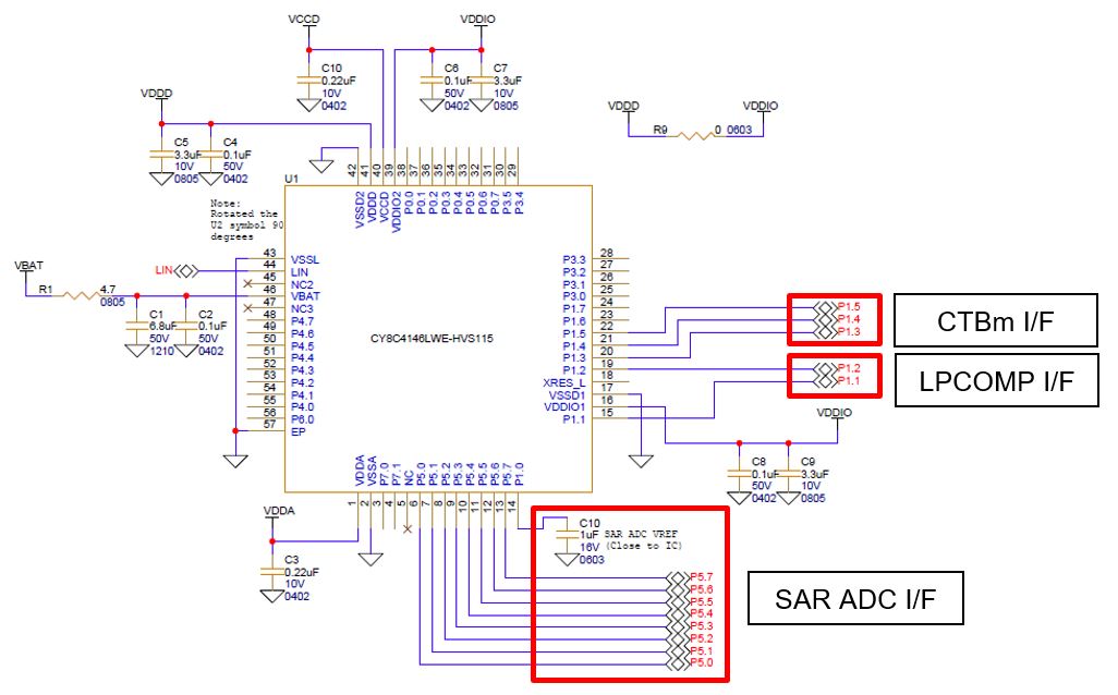
shows an example of external components.
Note: See AN234116 for details of external components of the power block.
Symbol | Overview | Parameter | ||
|---|---|---|---|---|
Value 1 | Value 2 | Value 3 | ||
C10 | SAR ADC bypass capacitor | 1 μF or 0.1 μF | X7R or more | > 10 V |
SAR ADC bypass capacitor
The internal references (1.2 V from bandgap or VDDA/2) are buffered with the reference buffer. This reference may be routed to the Ext Vref/SAR bypass pin where an external capacitor can be used to filter internal noise that may exist on the reference signal. The SAR ADC sample rate is limited to 100 ksps (at 12-bit sample rate) without an external reference bypass capacitor.
For example, without a bypass capacitor and with the 1.2 V internal Vref, the maximum SAR ADC clock frequency is 1.6 MHz. When using an external reference, it is recommended that an external capacitor is used.
Table 2
lists different reference modes and its maximum frequency/sample rate for 12-bit continuous mode operation.
Reference mode | Bypass capacitor | Buffer | Max frequency | Max sample rate (12-bit) |
|---|---|---|---|---|
1.2 V internal Vref | No | Yes | 1.6 MHz | 100 ksps |
Yes | Yes | 18 MHz | 1 Msps | |
VDDA/2 | No | Yes | 1.6 MHz | 100 ksps |
Yes | Yes | 18 MHz | 1 Msps | |
VDDA | No | No | 9 MHz | 500 ksps |
External Vref (low-impedance path) | No | No | 18 MHz | 1 Msps |
The startup time of the 1.2 V internal Vref varies with the bypass capacitor size;
Table 3
lists two common values for the bypass capacitor and the corresponding startup time specification for the internal Vref. If the reference selection is changed between scans or when scanning after sleep/deep sleep, make sure that the 1.2 V internal Vref is settled when the SAR ADC starts sampling. The worst-case settling time (when Vref is completely discharged) is the same as the startup time.
Internal Vref startup time | Maximum specification |
|---|---|
Startup time for reference with external capacitor (1 µF) | 2 ms |
Startup time for reference with external capacitor (0.1 µF) | 200 µs |
Startup time without external capacitor | 10 µs |
Layout example
shows an example of the power supply block layout.
Figure 6. Analog system block layout
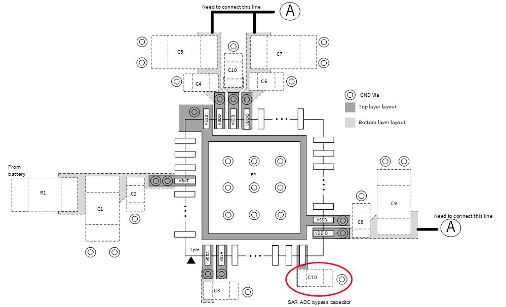
Follow these guidelines for the PSOC™ HV MS analog system circuit on the PCB:
Note: See AN234116 for detailed layout guidelines for the power block.
Place C10 (SAR ADC bypass capacitor) as close as possible to the pin. If the board has a GND plane, provide a through hole (via) near this capacitor.
If C10 is placed on the bottom side, provide a through hole (via) near the pin. Place C10 as close as possible to the through hole on the bottom side.
AutoPDL firmware configuration
Infineon provides an evaluation license of the Automotive Peripheral Driver Library (AutoPDL) including startup code as sample firmware. AutoPDL provides low-level drivers for all PSOC™ HV peripherals and is ISO 26262 compliant. AutoPDL has the following features:
Drivers and middleware
Low-level drivers for all peripherals
Middleware for complex peripherals such as CAPSENSE™
Qualified for ASPICE Level 2
MISRA 2012 AMD1, CERT C “Rules” (L1, L2, L3) are applied, Deviations/Warnings documented
Traceability
Safety ASIL-B
Safety documentation reduces customers’ effort for safety qualification
Safety features based on safety element out of context (SEooC)
Compiler version
IAR Embedded Workbench for Arm®, Functional Safety, version 8.50
Note: These examples are created based on AutoPDL version 1.3.1.
Analog system Peripheral Driver Library
The Peripheral Driver Library is a set of firmware drivers that provide APIs for accessing the hardware. These APIs perform initialization and control activities of each peripheral.
lists and describes the interface to each analog system function. The peripheral drivers of analog system are located in the AutoPDL path of:
<user path>\source\drivers\ sar, lpcomp, ctb
For more detailed information, see UsersGuide_xxxx _x_x_PSoC4HV_PDL.pdf in
<user path>\doc folder
.
Function | Description |
|---|---|
SAR ADC (cy_sar.h) | |
Cy_SAR_Init() | Initializes SAR ADC global control registers |
Cy_SAR_DeInit() | Deinitializes SAR ADC global control registers |
Cy_Sar_Enable() | Enables the SAR hardware |
Cy_Sar_Disable() | Disables the SAR hardware |
Cy_Sar_StartConvert() | Starts conversion immediately |
Cy_Sar_StopConvert() | Stops continuous conversion |
Cy_Sar_SetConvertMode() | Sets the registers SAMPLE_CTRL.DSI_TRIGGER_EN and DSI_TRIGGER_LEVEL |
Cy_Sar_GetInterruptStatusMasked() | Gets the INTR_MASKED register value |
Cy_Sar_GetResult16() | Gets the CHAN_RESULT.RESULT register value |
Cy_Sar_SetLowLimit() | Sets the RANGE_THRES.RANGE_LOW register value |
Cy_Sar_SetHighLimit() | Sets the RANGE_THRES.RANGE_HIGH register value |
Cy_Sar_SetAnalogSwitch() | Sets the MUX_SWITCH0 register value |
Cy_Sar_SetSwitchSarSeqCtrl() | Sets the MUX_SWITCH_HW_CTRL register value |
Cy_Sar_GetChanResultUpdated() | Gets the CHAN_RESULT_UPDATED register value |
Cy_Sar_EnableInjection | Sets the INJ_CHAN_CONFIG.INJ_START_EN register value |
Cy_Sar_SetRangeCond() | Sets the RANGE_COND register value |
Cy_Sar_SetDiagSwitch() | Sets the MUX_SWITCH2 register value |
Cy_Sar_SetDiagHwCtrl() | Sets the MUX_SWITCH_HW_CTRL2 register value |
Cy_Sar_GetInterruptStatus() | Gets the INTR register value |
Cy_Sar_ClearInterrupt() | Clears the INTR register value |
Cy_Sar_SetInterruptMask() | Sets the INTR_MASK register value |
Cy_Sar_GetRangeInterruptStatus() | Gets the RANGE_INTR register value |
Cy_Sar_ClearRangeInterrupt() | Clears the RANGE_INTR register value |
Cy_Sar_SetRangeInterruptMask() | Sets the RANGE_INTR_MASK register value |
Cy_Sar_GetRangeInterruptStatusMasked() | Gets the RANGE_INTR_MASKED register value |
Cy_Sar_GetSatInterruptStatus() | Gets the SATURATE_INTR register value |
Cy_Sar_ClearSatInterrupt() | Clears the SATURATE_INTR register value |
Cy_Sar_SetSatInterruptMask() | Sets the SATURATE_INTR_MASK register value |
Cy_Sar_GetSatInterruptStatusMasked() | Gets the SATURATE_INTR_MASKED register value |
Cy_Sar_GetInterruptCause() | Gets the INTR_CAUSE register value |
Cy_Sar_EnablePump() | Sets the PUMP_CTRL.ENABLED register value |
Cy_Sar_DisablePump() | Clears the PUMP_CTRL.ENABLED register value |
Cy_Sar_SetPumpClk() | Sets the PASS_CTRL register value |
Cy_Sar_InitChannel() | Sets the CHAN_CONFIG and CHAN_EN register value |
Cy_Sar_DeinitChannel() | Sets the initial value to CHAN_CONFIG and CHAN_EN register value |
Cy_Sar_EnableChannel() | Sets the CHAN_EN register value |
Cy_Sar_DisableChannel() | Clears the CHAN_EN register value |
Cy_Sar_GetInterruptMask() | Gets the INTR_MASK register value |
Cy_Sar_GetSatInterruptMask() | Gets the SATURATE_INTR_MASK register value |
Cy_Sar_GetRangeInterruptMask() | Gets the RANGE_INTR_MASK register value |
Cy_Sar_IsBusy() | Gets the SAR conversion status |
Cy_Sar_CalcDieTemp() | Converts the die temp measurement to degrees Celsius |
LPCOMP (cy_lpcomp.h) | |
Cy_Lpcomp_Init() | Initializes the low-power comparator |
Cy_Lpcomp_DeInit() | Deinitializes the low-power comparator |
Cy_Lpcomp_Start() | Enables the low-power comparator and sets the interrupt mode |
Cy_Lpcomp_Stop() | Disables the low-power comparator and sets the interrupt mode to disabled |
Cy_Lpcomp_ClearInterrupt() | Clears LPCOMP interrupts by setting each bit |
Cy_Lpcomp_GetInterruptSource() | Returns the status of two different LPCOMP interrupt requests |
Cy_Lpcomp_GetInterruptSourceMasked() | Returns an interrupt request register masked by an interrupt mask |
Cy_Lpcomp_GetCompare() | Returns a non-zero value when the voltage connected to the positive input is greater than the negative input voltage |
Cy_Lpcomp_SetInterruptMask() | Sets the LPCOMP interrupt mask by setting each bit |
Cy_Lpcomp_GetInterruptMask() | Returns an interrupt mask |
Cy_Lpcomp_SetSpeed() | Sets the drive power mode and speed configuration |
CTBm (cy_ctb.h) | |
Cy_Ctb_InitOpamp() | Initializes the opamp(s) |
Cy_Ctb_DeInit() | Resets the CTB registers back to power on reset defaults |
Cy_Ctb_Enable() | Powers up the CTB hardware block |
Cy_Ctb_Disable() | Powers down the CTB hardware block |
Cy_Ctb_SetDeepSleepMode() | Enables or disables the entire CTB (not per opamp) in deep sleep mode |
Cy_Ctb_SetPower() | Configures the power level and charge pump for the specific opamp(s) |
Cy_Ctb_SetCompInterruptEdgeType() | Sets the comparator edge detect for interrupt and output trigger |
Cy_Ctb_GetCompStatus() | Returns the comparator status |
Cy_Ctb_GetInterruptStatus() | Returns the status of the specified edge detect interrupt request |
Cy_Ctb_ClearInterrupt() | Clears the CTB comparator interrupt |
Cy_Ctb_SetInterruptMask() | Sets the specified interrupt mask value |
Cy_Ctb_GetInterruptMask() | Returns the specified interrupt mask value |
Cy_Ctb_GetInterruptStatusMasked() | Returns the CTB comparator edge output interrupt state after being masked |
Cy_Ctb_SetAnalogSwitch() | Open or close a set of the CTB switches |
Cy_Ctb_GetAnalogSwitch() | Returns the open or closed state of the specified analog switch(es) |
Cy_Ctb_OpenAllSwitches() | Opens all the switches and disables all hardware control of the switches |
Cy_Ctb_EnableSarSeqCtrl() | Enables the SAR sequencer control for the specified switches |
Cy_Ctb_DisableSarSeqCtrl() | Disables the SAR sequencer control for the specified switches |
Cy_Ctb_SetDsabSource() | Sets the DSAB bias current sources |
AutoPDL code example
To successfully execute the analog system examples, you need the following:
Evaluation kit (CYHVMS-64K-56-001 or KIT_PSOC4-HVMS-64K_LITE)
IAR EWARM 8.50.9 (or FS 8.50.10)
AutoPDL evaluation license or source code
SAR ADC example
This example demonstrates the SAR ADC single-channel measurement with single-ended input and averaging mode. The code example is located in the AutoPDL path of
<user path>\examples\sar
.
SAR ADC example configuration:
Channel: CH0 as single-ended (unsigned)
Resolution: maximum resolution (12-bit)
Target sample rate: 50 ksps (SAR clock 1 MHz, 18 clock cycles)
Acquisition time: 4 or 302 clock cycles
Averaging: enable (32 samples)
Diagnostic current sources and sink: Disable
Positive terminal: P5.3 (external temperature sensor)
Negative terminal: VSSA
Vref connection: VDDA
shows an example of SAR ADC configuration. For more details, see the architecture and register TRM in
References
.
Note: You should compare the code example with the flowchart and learn how to use the SAR ADC functions. You cannot copy/paste the code and expect it to work. This applies to all code examples provided in this document.
Code Listing 1
1 /* SAR channel configuration to use unsigned format. */
2	cy_stc_sar_channel_config_t config0_chan0_config =
3	{
4	  .sampleTimeSel         = CY_SAR_SAMPLE_TIME_SEL1,
5	  .posPinPortAddr        = CY_SAR_POS_ADDR_SARMUX_3,
6	  .avgEn                 = TRUE,
7	  .negPinPortAddr        = CY_SAR_NEG_ADDR_DIAG_VSSA,
8	  .resolution            = CY_SAR_MAXRESOLUTION,
9	  .differentialEn        = FALSE,
10	  .negAddrEn             = FALSE,
11	  .diagVplusSource       = FALSE,
12	  .diagVplusSink         = FALSE,
13	  .diagVminusSoure       = FALSE,
14	  .diagVminusSink        = FALSE,
15	};
16
17	/* SAR control configuration */
18	cy_stc_sar_control_config_t config0_ctrl0_config =
19	{
20
21	  /* SAMPLE_TIME01 register */
22	  /* Set the aperture times to target a 50 ksps scan rate.
23	  * Recall that the SAR clock is 1 MHz.
24	  * Sample Time 0 is set to 302 clock cycles.
25	  * Sample Time 1 is set to 4 clock cycles. */
26	  .sampleTime0           = 302,
27	  .sampleTime1           = 4,
28
29	  /* SAMPLE_TIME23 register */
30	  /* Set the unused sample times 2 and 3 to be 4 clock cycles.
31	  * Note that these two sample times are not used by any channels and only shown for reference */
32	  .sampleTime2           = 4,
33	  .sampleTime3           = 4,
34	  .rangeCond             = CY_SAR_RANGE_COND_BELOW,
35
36	  /* Set the initial state of switches.
37	  * Close the switch between Pin 3 of the SARMUX to the positive terminal of the SAR (used by channel 3).
38	  * Close the switch between VSSA and the negative terminal of the SAR (VSSA_VMINUS). */
39	  .sarmuxFirmwareSwitches = CY_SAR_MUX_FW_P3_VPLUS_MSK | CY_SAR_MUX_FW_VSSA_VMINUS_MSK,
40
41	  .singleEndedSigned     = FALSE,
42	  .vrefSel               = CY_SAR_VREF_SEL_VDDA,
43	  .negSel                = CY_SAR_NEG_SEL_VSSA_KELVIN,
44	  .sarHwCtrlNegvref      = CY_SAR_NEGVREF_FW_ONLY,
45	  .pwrCtrlvref           = CY_SAR_NORMAL_PWR,
46	  .icontLv               = CY_SAR_LV_NORMAL_PWR,
47	  .subResolution         = CY_SAR_SUB_RESOLUTION_10B,
48	  .avgCnt                = CY_SAR_AVG_CNT_32,
49	  .avgMode               = CY_SAR_ACCUNDUMP,
50	  .trigMode              = CY_SAR_TRIGGER_MODE_FW_ONLY,
51	  .vrefBypCapEn          = TRUE ,
52	  .boostpumpEn           = FALSE,
53	  .refbufEn              = TRUE,
54	  .switchDisable         = TRUE,
55	  .leftAlign             = FALSE,
56	  .differentialSigned    = FALSE,
57	  .avgShift              = TRUE,
58	  .dsiSyncTrigger        = FALSE,
59	  .eosDsiOutEn           = FALSE,
60	};
shows the flowchart for SAR ADC design;
Code Listing 2
shows the main function.
Figure 7. Flowchart for SAR ADC example
Code Listing 2
1	/* Function Name: main */
2	int main(void)
3	{
4	    SystemInit();
5
6	    __enable_interrupt(); /* Enable global interrupts. */
7
8	    /* Initialize Port and Clock */
9	    Peripheral_Initialization();
10
11	    /* Opening UART Comment */
12	    TERM_PRINT_H("SAR ADC Code example \n\r");
13
14	    /* Initialize the SAR positive port */
15	    Cy_Gpio_SetDriveMode(CY_USER_PORT, CY_USER_PIN, CY_GPIO_DRIVE_MODE_ANALOG);
16
17	    /* Configure the clock for the SAR for a 1 MHz clock frequency. */
18	    Cy_SysClk_Periph_AssignDivider(CY_PCLK_PASS0_CLOCK_SAR, CY_SYSCLK_DIV_16_BIT, 1u);
19	    Cy_SysClk_Periph_SetDivider(CY_SYSCLK_DIV_16_BIT, 1u, SAR_TARGET_CLK_DIVIDER - 1u);
20	    Cy_SysClk_Periph_EnableDivider(CY_SYSCLK_DIV_16_BIT, 1u);
21
22	    /* Interrrupt Configuration for WDT */
23	    Cy_SysInt_SetVector(pass_0_interrupt_sar_IRQn, SAR_Interrupt);
24	    Cy_SysInt_ClearPendingIRQ(pass_0_interrupt_sar_IRQn);
25	    Cy_SysInt_EnableIRQ(pass_0_interrupt_sar_IRQn);
26
27	    /* De-initialize and enable the SAR to Config0. */
28	    Cy_Sar_DeInit(CY_SAR0);
29
30	    /* Initialize the SAR block to Config0. */
31	    Cy_Sar_Init(CY_SAR0, &config0_ctrl0_config);
32
33	    /* Set interrupt mask for the SAR sources */
34	    Cy_Sar_SetInterruptMask(CY_SAR0, CY_SAR_INTR_EOS_INTR_MSK);
35
36	    /* Enable the SAR block to Config0. */
37	    Cy_Sar_Enable(CY_SAR0);
38	    // Wait 2 [ms]
39	    Cy_SysLib_DelayUs(2000);
40
41	    /* Initialize and enable the SAR channel to Config0 channel 0. */
42	    Cy_Sar_InitChannel(CY_SAR0, 0, &config0_chan0_config);
43	    Cy_Sar_EnableChannel(CY_SAR0, CONFIG0_CHAN_EN);
44
45	    /* Initiate continuous conversions. */
46	    Cy_Sar_StartConvert(CY_SAR0, CY_SAR_CONVERT_MODE_CONTINUOUS);
47
48	    for(;;)
49	    {
50	        // Wait 0.5 [s]
51	        Cy_SysLib_Delay(500);
52
53	        /* Printing SAR(ADC) values in UART terminal */
54	        Term_Printf("ADC conversion value for Potentiometer : %d \n\r", chanResult);
55	    }
56	}
57
58	/* Function Name: SAR_Interrupt */
59	void SAR_Interrupt(void)
60	{
61	    uint32 intrStatus = 0u;
62
63	    /* Read interrupt status register. */
64	    intrStatus = Cy_Sar_GetInterruptStatus(CY_SAR0);
65
66	    /* Check for the EOS interrupt. */
67	    if ((intrStatus & CY_SAR_INTR_EOS_INTR_MSK) == CY_SAR_INTR_EOS_INTR_MSK)
68	    {
69	        /* Clear handled interrupt. */
70	        Cy_Sar_ClearInterrupt(CY_SAR0, intrStatus);
71
72	        /* Get the ADC results for connected channel in Config0. */
73	        chanResult = Cy_Sar_GetResult16(CY_SAR0, 0);
74	    }
75	}
Low-power comparator example
This example demonstrates the LPCOMP0_CH0 single-channel measurement with differential input on +ve (P1.1) and -ve (P1.2) terminals. The comparator value of LPCOMP is available in the
lpcompCmpValue
variable; the signal can be output to any GPIO. The code example is located in AutoPDL path of
<user path>\examples\lpcomp
.
Note: Pin assignment differs between this example and the AutoPDL example file.
LPCOMP example configuration:
Channel: LPCOMP[0]CH0 as single-channel measurement
Power mode: Slow operating mode (uses less power, <50 µA)
Hysteresis: Enable (add 10 mV hysteresis)
Interrupt type: Both rising and falling edges
Comparator DSI (trigger) out: Synchronize and level
shows the example of LPCOMP configuration. For more details, see the architecture and register TRMs in
References
.
Code Listing 3
1	/* Configuration structure for channel of low-power comparator */
2	cy_stc_lpcomp_config_t user_lpcomp_ch_cfg =
3	{
4	    .outputMode = CY_LPCOMP_OUT_SYNC,   // CY_LPCOMP_OUT_DIRECT,
5	    .hysteresis = CY_LPCOMP_HYST_ENABLE,
6	    .speed      = CY_LPCOMP_MODE_SLOW,
7	};
shows the flow chart for LPCOMP design, and
Code Listing 4
shows the code example of main function.
Figure 8. Flowchart for LPCOMP example
Code Listing 4
1	/* Function Name: main */
2	int main(void)
3	{
4	    SystemInit();
5
6	    __enable_interrupt(); /* Enable global interrupts. */
7
8	    /* Initialisation of User Led */
9	    Cy_Gpio_SetPinMode(CY_USER_LED1_PORT_IDX, CY_USER_LED1_PIN, CY_USER_LED1_MUX);
10	    Cy_Gpio_SetDriveMode(CY_USER_LED1_PORT_IDX, CY_USER_LED1_PIN, CY_GPIO_DRIVE_MODE_OD_DRIVE_HIGH);
11
12	    /* Initialisation of low-power comparator input */
13	    Cy_Gpio_SetPinMode(USER_LPCOMP_POS_IN_PORT, USER_LPCOMP_POS_IN_PIN, USER_LPCOMP_POS_IN_PIN_MUX);
14	    Cy_Gpio_SetDriveMode(USER_LPCOMP_POS_IN_PORT, USER_LPCOMP_POS_IN_PIN, CY_GPIO_DRIVE_MODE_ANALOG);
15
16	    Cy_Gpio_SetPinMode(USER_LPCOMP_NEG_IN_PORT, USER_LPCOMP_NEG_IN_PIN, USER_LPCOMP_NEG_IN_PIN_MUX);
17	    Cy_Gpio_SetDriveMode(USER_LPCOMP_NEG_IN_PORT, USER_LPCOMP_NEG_IN_PIN, CY_GPIO_DRIVE_MODE_ANALOG);
18
19	    /* Initialisation of low-power comparator output */
20	    Cy_Gpio_SetPinMode(USER_LPCOMP_OUT_PORT, USER_LPCOMP_OUT_PIN, USER_LPCOMP_OUT_PIN_MUX);
21	    Cy_Gpio_SetDriveMode(USER_LPCOMP_OUT_PORT, USER_LPCOMP_OUT_PIN, CY_GPIO_DRIVE_MODE_PULLUP);
22
23	    /* De-initializes the low-power comparator */
24	    Cy_Lpcomp_DeInit(LPCOMP_INSTANCE, LPCOMP_CHANNEL);
25
26	    /* Initializes the low-power comparator */
27	    Cy_Lpcomp_Init(LPCOMP_INSTANCE, LPCOMP_CHANNEL, &user_lpcomp_ch_cfg);
28
29	    /* Enable low-power comparator */
30	    Cy_Lpcomp_Start(LPCOMP_INSTANCE, LPCOMP_CHANNEL, LPCOMP_INTERRUPT);
31
32	    /* Set irq for low-power comparator interrupt */
33	    Cy_SysInt_SetVector(LPCOMP_IRQ, LpcompEventHandler);
34	    Cy_SysInt_ClearPendingIRQ(LPCOMP_IRQ);
35	    Cy_SysInt_EnableIRQ(LPCOMP_IRQ);
36
37	    /* Set interrupt mask for the lpcomp sources */
38	    Cy_Lpcomp_ClearInterrupt(LPCOMP_INSTANCE, LPCOMP_INTR_MASK);
39	    Cy_Lpcomp_SetInterruptMask(LPCOMP_INSTANCE, LPCOMP_INTR_MASK);
40
41	    /* Check blinking rate of RED Led */
42	    for(;;)
43	    {
44	        // Wait 0.05 [s]
45	        Cy_SysLib_DelayUs(50000);
46	        Cy_Gpio_Inv(CY_USER_LED1_PORT_IDX, CY_USER_LED1_PIN);
47	    }
48	}
49
50	/* Function Name: intrupput */
51	void LpcompEventHandler(void)
52	{
53	    uint32 intStatus;
54
55	    /* Get the current status of LPCOMP interrupts */
56	    intStatus = Cy_Lpcomp_GetInterruptSource(LPCOMP_INSTANCE);
57
58	    if(intStatus & LPCOMP_INTR_MASK)
59	    {
60	        /* Get the LPCOMP channel compare value */
61	        lpcompCmpValue = Cy_Lpcomp_GetCompare(LPCOMP_INSTANCE, LPCOMP_CHANNEL);
62	    }
63
64	    /* Clear the LPCOMP interrupt */
65	    Cy_Lpcomp_ClearInterrupt(LPCOMP_INSTANCE, intStatus);
66	}
Continuous-time block mini example
This example demonstrates the comparator and amplifier functions of continuous-time block mini (CTBm) by using AutoPDL. The comparator compares the input voltage of P1.1 and P1.6. The amplifier amplifies the input voltage at P1.7 with 2x magnification.
Note: There is no code example in the AutoPDL package.
CTBm example configuration:
Comparator
Power level: High-power mode
Opamp output mode: Comparator mode
Comparator edge detection: Both edge detection
Comparator trigger mode: Output pulse
Trigger output: Synchronize
Comparator hysteresis: Enable 10 mV hysteresis
Opamp charge pump: Enable
Deep sleep mode: Disable
Amplifier
Power level: High-power mode
Opamp output mode: Amplifier mode
Opamp charge pump: Enable
Deep sleep mode: Disable
Other comparator settings: Default
shows the example of CTBm configuration. For more details, see the architecture and register TRMs in
References
.
Code Listing 5
67	/* Comparator configuration structure */
68	cy_stc_ctb_opamp_config_t Ctb_Control_Config = {
69	  .switchCtrl = TEST_CTB_COMPARATOR0_SWITCH_MASK,
70	  .power      = CY_CTB_POWER_HIGH,
71	  .outputMode = CY_CTB_MODE_COMP,
72	  .compEdge   = CY_CTB_COMP_EDGE_BOTH,
73	  .compLevel  = CY_CTB_COMP_TRIGGER_OUT_PULSE,
74	  .compBypass = FALSE,
75	  .compHyst   = TRUE,
76	  .pump       = TRUE,
77	};
78
79	/* Amplifier configuration structure */
80	cy_stc_ctb_opamp_config_t Ctb_Control_Config = {
81	  .switchCtrl = TEST_CTB_AMPLIFIER1_SWITCH_MASK,
82	  .power      = CY_CTB_POWER_HIGH,
83	  .outputMode = CY_CTB_MODE_OPAMP_INTERNAL,
84	  .compEdge   = CY_CTB_COMP_EDGE_DISABLE,
85	  .compLevel  = CY_CTB_COMP_TRIGGER_OUT_PULSE,
86	  .compBypass = FALSE,
87	  .compHyst   = FALSE,
88	  .pump       = TRUE,
89	};
shows the flow chart for CTBm design, and
Code Listing 6
shows the code example of main function.
Figure 9. Flowchart for CTBm example
Code Listing 6
90	/* Function Name: main */
91	int main(void)
92	{
93	  SystemInit();
94
95	  /* Enable global interrupts. */
96	  __enable_interrupt();
97
98	  Peripheral_Setup();
99
100	  Comparator0_Sequence(); /* Configure opamp0 as comparator */
101	  Amplifier1_Sequence();  /* Configure opamp1 as amplifier  */
102
103	  Cy_Ctb_SetDsabSource(CY_PASS0, CY_CTB_DSAB_ACTIVE); /* Active mode             */
104	  Cy_Ctb_SetDeepSleepMode(CY_CTBM0, FALSE);           /* Disable deep sleep mode */
105
106	  Cy_Ctb_Enable(CY_CTBM0); /* Enable CTB                          */
107	  Cy_SysLib_Delay(1u);     /* Wake-up time from Enabled to Usable */
108
109	  /* Enable comparator0 interrupt */
110	  Cy_Ctb_ClearInterrupt(CY_CTBM0, CY_CTB_OPAMP_0);   /* Clear comparator0 interrupt       */
111	  Cy_Ctb_SetInterruptMask(CY_CTBM0, CY_CTB_OPAMP_0); /* Enable comparator0 interrupt mask */
112
113	  for(;;)
114	  {
115	    Cy_SysLib_Delay(1000);
116	  }
117	}
118
119	/* Function Name: intrupput */
120	void DEFAULT_CTB_HANDLER(void)
121	{
122	  uint32 intrStatus = Cy_Ctb_GetInterruptStatus(CY_CTBM0, CY_CTB_OPAMP_BOTH);
123
124	  /* OpAmp0 comparator edge detect interrupt */
125	  if (CY_CTB_INTR_COMP0_MSK == (CY_CTB_INTR_COMP0_MSK & intrStatus))
126	  {
127	    Cy_Ctb_ClearInterrupt(CY_CTBM0, CY_CTB_OPAMP_0); /* Clear interrupt */
128	  }40	}
CTBm connects to SAR ADC
The SAR ADC inputs are from the external pin (only for eight channels in single-ended mode and four channels in differential mode) or an internal signal (AMUXBUS/CTBm/temperature sensor/diagnostic inputs).
This example demonstrates how to connect the CTBm output via the sarbus0/1 input of SARMUX, which is a programmable analog multiplexer (see
Figure 10
).
Note: CTBm sampling time is not fast enough to sample at 1 Msps.See the architecture TRM for more detailed SARMUX information.
Figure 10. SARMUX block diagram
shows an example of the SAR ADC channel configuration and amplifier switch mask definition. See Section
SAR ADC example
for SAR ADC configuration details and Section
Continuous-time block mini example
for CTBm configuration details.
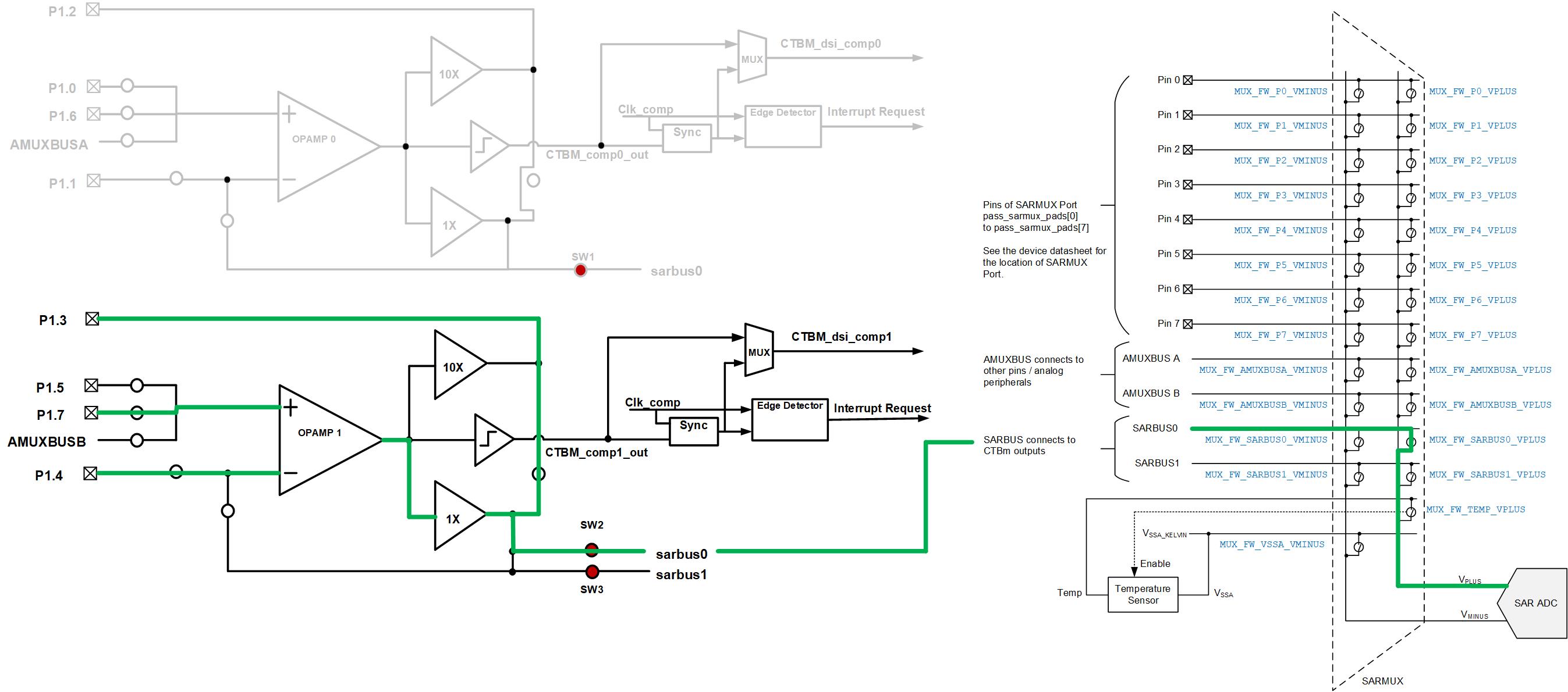
Code Listing 7
1	/* SAR ADC channel configuration*/
2	static cy_stc_sar_channel_config_t Sar_channel_config =
3	{
4	  .posPinPortAddr  = CY_SAR_POS_ADDR_CTB0_OA1, /* POS select CTB0 opamp1            */
5	  .resolution      = CY_SAR_MAXRESOLUTION,     /* 12-Bit resolution                 */
6	  .sampleTimeSel   = CY_SAR_SAMPLE_TIME_SEL0,  /* Sample time 0                     */
7	  .negPinPortAddr  = CY_SAR_NEG_ADDR_SARMUX_0, /* Default negative port/pin address */
8	  .differentialEn  = FALSE,                    /* Disable differential              */
9	  .avgEn           = TRUE,                     /* Enable average                    */
10	  .negAddrEn       = FALSE,                    /* Disable negative port/pin address */
11	  .diagVplusSource = FALSE,                    /* Disable VPLUS pullup              */
12	  .diagVplusSink   = FALSE,                    /* Disable VPLUS pulldown            */
13	  .diagVminusSoure = FALSE,                    /* Disable VMINUS pullup             */
14	  .diagVminusSink  = FALSE,                    /* Disable VMINUS pulldown           */
15	};
16
17	/* amplifier1SwitchMask */
18	#define TEST_CTB_AMPLIFIER1_SWITCH_MASK (CY_CTB_OA1_SW_OA1P_A43_MSK | \
19	                                         CY_CTB_OA1_SW_OA1M_A22_MSK | \
20	                                         CY_CTB_OA1_SW_OA1O_D52_MSK | \
21	                                         CY_CTB_OA1_SW_OA1O_D82_MSK)
22
23	#define TEST_CTB_AMPLIFIER1_SEQ_SWITCH_MASK (CY_CTB_SW_HW_CTRL_P2_MSK | CY_CTB_SW_HW_CTRL_P3_MSK)
posPinPortAddr = CY_SAR_POS_ADDR_CTB0_OA1
sets the positive port of the SAR ADC (select CTB0 opamp1).
TEST_CTB_AMPLIFIER1_SWITCH_MASK
controls the CTBm internal switches as shown below (0=open, 1=close switch).
CY_CTB_OA1_SW_OA1P_A43_MSK
: Opamp1 positive terminal ctbbus1
CY_CTB_OA1_SW_OA1M_A22_MSK
: Opamp1 negative terminal P4
CY_CTB_OA1_SW_OA1O_D52_MSK
: Opamp1 output sarbus0 (ctbbus2 in CTB)
CY_CTB_OA1_SW_OA1O_D82_MSK: Opamp1 output switch to short 1x with 10x drive
shows the internal switches setting of this example.
Note: The negative port is connected to Vref by the SAR ADC configuration.See Section SAR ADC example to learn how to get the SAR ADC results.
Figure 11. Internal switches setting
Summary
This application note described the details of the analog system block of PSOC™ HV MS MCU. By using the analog system block, human-machine interface (HMI), body, and powertrain applications can be achieved with higher quality.
Infineon provides an evaluation board and wealth of sample software to help you get started with PSOC™ HV MS family MCUs. To use the evaluation board, contact your sales representative or Infineon Technical Support.
Glossary
Terms | Description |
|---|---|
ADC | analog-to-digital converter |
AHB | Advanced High-performance Bus |
AMUX | analog multiplexer |
API | application programming interface |
AutoPDL | Automotive Peripheral Driver Library |
ASIL-B | Automotive Safety Integrity Level – B |
ASPICE | Automotive Software Process Improvement and Capability Determination |
CERT | Computer Emergency Response Team |
CPU | central processing unit |
CTBm | Continuous-time block mini |
CTRL | Control |
CTRLMUX | control multiplexer |
DIAGMUX | diagnostic multiplexer |
DIAG cur SRC/SINK | diagnostic current sources and sinks |
DMA | direct memory access |
EXPMUX | expansion multiplexer |
FW | firmware |
GND | Ground |
GPIO | general-purpose I/O |
GUI | graphical user interface |
HFCLK | high-frequency clock |
HMI | human-machine interface |
HV | high-voltage |
HW | hardware |
I/O | input or output |
I/F | Interface |
IAR | IAR Systems (company name) |
IAR EARM | IAR Embedded Workbench for Arm® (software name) |
IC | integrated circuit |
ISO | International Organization for Standardization |
LED | light-emitting diode |
LIN | Local Interconnect Network |
LPCOMP | Low-power comparator |
MUX | Multiplexer |
MW | middleware |
MSC | multi-sense converter |
MCU | microcontroller unit |
MISRA | Motor Industry Software Reliability Association |
MS | mixed signal |
PCB | printed circuit board |
PELI | peripheral |
pF | picofarad |
PHY | physical layer |
PWM | pulse width modulation |
QFN | quad flat non-leaded |
RX | receiver |
SAR | successive approximation register |
SARMUX | SAR multiplexer |
SARREF | SAR reference |
SARSEQ | SAR sequencer |
SEooC | safety element out of context |
SW | switch |
TRM | technical reference manual |
TX | transmitter |
References
Application notes
Infineon Technologies AG:
AN185951 PSOC™ 4 and PSOC™ 6 MCU CAPSENSE™ design guide
; Available online
Infineon Technologies AG:
AN234115 - Getting started with PSOC™ HV MS family
; Available online
Infineon Technologies AG:
AN234116 - Hardware design guide for PSOC™ HV MS family
; Available online
Infineon Technologies AG:
AN0003 - High voltage subsystem (HVSS) in PSOC™ HV MS family
; Available online
Infineon Technologies AG:
AN0005 - CAPSENSE™ (multi-sense converter) block in PSOC™ HV MS family
; Available online
Device datasheet
Infineon Technologies AG:
PSOC™ High Voltage (HV) Mixed Signal (MS) Automotive MCU datasheet
; Available online
Architecture reference manual
Infineon Technologies AG:
PSOC™ high voltage (HV) mixed signal (MS) MCU architecture technical reference manual (TRM)
; Available online
Registers reference manual
Infineon Technologies AG:
PSOC™ high-voltage (HV) mixed signal (MS): PSOC(TM) HVMS-64K registers TRM
; Available online
Infineon Technologies AG:
PSOC™ high-voltage (HV) mixed signal (MS): PSOC(TM) HVMS-128K registers TRM
; Available online
Evaluation board user guide
Infineon Technologies AG:
CYHVMS-64K-56-001 PSOC™ high-voltage (HV) mixed signal (MS) evaluation kit user guide
; Available online
Automotive peripheral driver library (AutoPDL)
Infineon Technologies AG:
PSOC™ HV MS AutoPDL
; Available online
Revision history
Document version | Date of release | Description of changes |
|---|---|---|
V1.0 | 2025-06-26 | Initial release |
Trademarks
PSOC™, formerly known as PSoC™, is a trademark of Infineon Technologies. Any references to PSoC™ in this document or others shall be deemed to refer to PSOC™.