AN0003 High-voltage subsystem (HVSS) in PSOC™ HV MS family
About this document
Scope and purpose
This application note gives an introduction to the high-voltage subsystem (HVSS) of the PSOC™ HV mixed signal (MS) family. This application note also provides guidance in developing HVSS hardware and firmware designs.
Intended audience
This document is intended for hardware and firmware design engineers using PSOC™ HV MS family MCUs.
Introduction
PSOC™ HV MS (64 K/ 128 K) belongs to the PSOC™ high voltage (HV) mixed signal (MS) series of products. It is a fully integrated programmable embedded system for automotive HMI, body, and powertrain applications. The system features an Arm® Cortex®-M0+ processor with programmable and reconfigurable analog and digital blocks. The system consists of –
microcontroller with a 12-bit SAR ADC
fifth generation multi-sense converter (MSC) block supporting capacitive sensing (CAPSENSE™)
digital peripherals such as PWMs and serial communication interfaces
selectable LIN/CXPI interface with integrated PHY
high-voltage subsystem to operate directly off the 12 V car battery
HVSS overview
The PSOC™ HV MS high-voltage subsystem (HVSS) contains a series of power management circuits used in automotive applications. With the usage of HVSS, automotive batteries can be connected directly with tolerance up to 42 V. The HVSS has the following features:
HVSS circuits operate directly from a 12-V or a 24-V automotive battery (tolerates up to 42 V)
A high-voltage linear regulator (HVREG) operating from a car battery voltage delivering 3.3 V or 5 V nominal core voltage –
Regulator output voltage: 3.3 V or 5 V (selectable by ordering code) with ± 2% trimmed accuracy
Minimum output voltage: 2.7 V (VBAT > 3.6 V), 3.3 V (VBAT > 4.3 V), 5 V (VBAT > 6 V)
Regulator current: up to 60 mA; 20 μA of maximum quiescent current at room temperature in Deep Sleep mode
VBAT voltage divider (VDIV), ratio of 24, and resistance of at least 200 KΩ
Thermal shutdown (nominal 170°C) and release (nominal 130°C)
Foldback current limiting (100 – 200 mA)
Power good function
LIN/CXPI physical interface transceiver (PHY) –
Data rates up to 20 kbps with high EM noise immunity
Positive/negative DC tolerance for LIN/CXPI pin: –27 V to 42 V
Sleep mode current consumption: I VBAT + I VDDD = maximum of 10 µA
Programmable slew rate control: 1.0 V/1.5 V/2.0 V per µs at VBAT = 12 V
Dominant timeout and LIN wakeup interrupt timers (CXPI ignore the wakeup timer value)
An AHB bus interface and control and status registers
Interrupt logic
shows the block diagram of a HVSS.
Figure 1. HVSS block diagram
HVREG
The high-voltage regulator (HVREG) has self-start from the battery, without a reference voltage; it provides 3.3 V or 5 V to VDDD and VDDA as chip supply. The voltage is selectable by ordering code (see PSOC™ HV MS datasheet
3
). It also contains a power good function and a Zener diode on the output pin for over-voltage protection. The HVREG operates with stability against automotive battery voltage transient events, keeping the output voltage even if the VBAT pin drops in cold cranking or rises in a load dump surge.
The HVREG also provides thermal shutdown (TSD) and VBAT voltage divider (VDIVIDER) functions. The TSD shunts off HVREG or send notification to CPU when junction temperature reaches to 170 °C. The VDIVIDER is a voltage divider to scale battery voltage (VBAT) to levels compatible with on-chip ADC; this ensures that battery voltages are measured.
LIN/CXPI PHY
The local interconnect network (LIN)/clock extension peripheral interface (CXPI) physical interface transceiver (PHY), is the interface between protocol controllers and physical bus, which meets the requirements of LIN standard 2.2A and CXPI ISO/WD 20794.
The LIN PHY also is downward-compatible with LIN 2.0. It supports data rates of 1 to 20 Kbps. Non-LIN fast slew rates are available, providing 100 Kbps data rates for fast downloads; this is used for factory and field flash program updates using the LIN pin.
HVREG
The following sections describe the high-voltage regulator (HVREG) architecture, HVREG I/O pins, and HVREG operating conditions.
Block description
The block diagram of the master regulator is shown in
Figure 2
.
The master regulator includes a control interface (level shifters, and so on), a voltage reference, bias circuitry, a thermal shutdown detector (TSD), a VBAT voltage divider (divided by 24), and the regulator core (output driver, feedback loop, error amplifier, and overcurrent detection). The core is able to supply up to 60 mA load current. The output voltage is selectable for 3.3 V or 5 V (± 2%) with VBAT more than 6 V for 5 V output setting, or 4.3 V for 3.3 V output setting. When VBAT drops less than 6 V for 5 V setting, or 4.3 V for 3.3 V setting, its output voltage is dropped depending on VBAT voltage.
This regulator provides VDDD (and VDDA, VDDIO) which is used to power the chip. This regulator is always powered on and can select either “normal mode” or “Deep Sleep mode” with “en_deepsleep” pin. Note that the VCCD (1.8 V) regulator is included in the system resources subsystem (SRSS).
Figure 2. HVREG block architecture and function diagram
HVREG input pins
The following section describes the HVREG input pins.
en_hv
is a reset signal input pin which is routed by internal signal. While this pin is in “L”, internal level shifters are in reset. At this time, the trimming code is set to the default (all “0”). When this pin is set to “H” (and the cell's pg_hv pin is “H”), HVREG can accept the input signals from trim bus line. The pg_hv pin works with en_hv to cover any uncertainty in the en_hv signal at low VDDD
vddd_s
is an analog input pin to sense VDDD voltage level by VDDD PAD remotely. This pin appropriately connects to VDDD PAD to suppress the load regulation fluctuation due IR drop
vout_sel
(selectable by ordering code) is an input signal to select VDDD output voltage target
en_deepsleep
(control by SRSSHV.POWER_MODE) is an input signal pin to enable Deep Sleep mode (H: deepsleep, L: normal)
enb_zener and en_ndiode (HVSS_HVREG_CTRL.Zener_Clamp_Mode) are input signal pins to control Zener diode active/inactive state and NMOS diode active/inactive state
vddd_trim<5:0>
(HVSS_HVREG_TRIM) is an input bus for trimming adjustment of the VDDD output voltage. While en_hv is in “H”, HVREG output voltage can be adjusted.
vref_trim<5:0>
(HVSS_HVREG_TRIM_VREF) is an input bus for trimming adjustment of the V ref output voltage, which is the internal reference voltage for the amplifier of the regulator and TSD V th ladder resistor. While en_hv is in “H”, this local V ref output voltage can be adjusted.
vref_tc_trim<5:0>
(HVSS_HVREG_TRIM_VREF_TC) is an input bus for trimming adjustment of the Vref output voltage temperature coefficient, which is about the temperature coefficient of the internal reference voltage for the amplifier of the regulator and TSD Vth ladder resistor. While en_hv is in "H", this local V ref output voltage can be adjusted.
tsd_trim<5:0>
(HVSS_HVREG_TRIM_TSD) is an input bus for trimming adjustment of TSD detection temperature. While en_hv is in “H”, TSD detection temperature can be adjusted
enb_tsd and enb_tsd_shutoff (HVSS_HVREG_CTRL.TSD_Mode) are input signal pins to enable thermal shut down and HVREG shutoff function when TSD is detected
rdiv_en
(HVSS_HVREG_CTRL.EN_VDIV) is an input signal pin for divider enable (0x0: inactive, 0x1: active)
vdiv_ret
is a ground input pin
HVREG output pins
The following section describes the HVREG output pins.
vddd
is the output pin of this regulator, a nominal 3.3 V or 5 V regulated voltage is selectable with loads up to 60 mA. This output drives the chip's VDDD, VDDA and VDDIO that through the GPIO can drive external loads. The VDDD pin is always on after completing the start up
pg_hv
is the output pin of power good circuit in HVREG. HVREG monitors the VDDD output voltage net. When VDDD is lower than 2.0 V, “pg_hv” provides a secure “L”. Hence, this output signal can work as the reset signal of SRSS (BODHVSS) whole chip in the voltage range lower than VDDD = 2.0 V
pg_lv
is the output pin of power good output as a status signal for internal logic
amuxbusa
is the output pin for test. Internal nodes can be monitored on this pin in test modes
tsd_out
is the output pin for TSD to notify temperature status as “H” to the logic circuit block when TSD detects chip junction temperature higher than 170 °C (nominal). After the chip junction temperature is lower than 130 °C (nominal), “tsd_out" will return to "L"
vs0_in_p
is the output pin of the VBAT divided voltage
vs0_in_n
is the output low reference voltage for the dividers, intended to be used as the ADC negative input. Alternately, this function can use “vdiv_ret", which is the ground of this resistor ladder attenuator
Operating voltage
and
Table 2
show the HVREG absolute maximum ratings and operating conditions respectively.
Note: The following values are based on the PSOC™ HV MS datasheet (version 002-33200*D). See 3 for latest values.
Parameter | Description | Min | Typ | Max | Units | Details/conditions |
|---|---|---|---|---|---|---|
V BAT | Supply voltage V BAT | – 0.3 | – | 42 | V | |
I BAT | V BAT supply current | – | – | 160 | mA | |
I BATABSDC | V BAT supply current, long-term average | – | – | 60 | mA |
Parameter | Description | Min | Typ | Max | Units | Details/conditions |
|---|---|---|---|---|---|---|
V BAT | Battery supply voltage V BAT | 3.6 | – | 28 | V | |
V DDX | 5-V output voltage setting; V BAT > 6 V | 4.9 | 5 | 5.1 | V | |
V DDX | 5-V output voltage setting; 6 V ≥ V BAT ≥ 3.6 V | 2.7 | – | 5.15 | V | |
V DDX | 3.3-V output voltage setting; V BAT > 4.3 V | 3.234 | 3.3 | 3.366 | V | |
V DDX | 3.3-V output voltage setting; 4.3 V ≥ V BAT ≥ 3.6 V | 2.7 | – | 3.39 | V | |
I DDD | Digital regulator current | – | – | 60 | mA | Typical internal loads = 30 mA + external loads from V DDD = 30 mA |
LIN/CXPI PHY
The following sections describe the LIN/CXPI PHY – architecture, I/O pins, and operating conditions.
Block description
The LIN/CXPI driver includes slew control to maintain consistent duty cycle over a range of loads. It also includes turn-on/turn-off control to reduce impact from incoming EMI. Large amounts of RF energy can be present in the LIN/CXPI bus; the driver must remain functional in the presence of this energy. Hence, special attention is required to design feedback circuits to avoid their saturation in the presence of RF energy.
LIN/CXPI receiver thresholds are specified in relation to the supply voltage VBAT. A comparator with voltage dividers sets the receiver threshold and scales bus voltages to appropriate levels. Noise filtering is needed to prevent RF energy and brief transients from disturbing communication.
The LIN/CXPI specification has certain isolation requirements to ensure that the LIN/CXPI bus is not compromised by certain faults. This includes ensuring that the loss of supply voltage or ground of a slave node does not affect LIN/CXPI communication between other nodes. This requirement hence introduces reverse protection diodes in series with pullup resistors and another diode in series with the open-drain pull-down resistor. This prevents powering components from the LIN/CXPI bus, and excessively loading the LIN/CXPI bus and disrupting communication.
shows the LIN/CXPI PHY transceiver block diagram.
Figure 3. LIN/CXPI block diagram
Note: All register/function names follow the “LIN” nomenclature. Even if interface mode sets as “CXPI”, the register/function uses the name of “LIN”.
LIN/CXPI input pins
pg_hv
input functions as cell reset signal. When “pg_hv” is low, the cell is reset. This disables the cell and sets level shifters to their default states. These are VDDD-level signals
sel_cxpi_lin<1:0>
(HVSS_LIN_CTL.SEL_CXPI_LIN<2:0>) is an input to select LIN or CXPI PHY interface. Bit ‘0’ selects LIN while bit ‘1’ selects CXPI master or slave
lin_mode<2:0>
(HVSS_LIN_CTL.LIN_MODE<2:0>) is an input to change the LIN/CXPI PHY function mode. These modes are described in Table 6 .
txd
is the data input signal, giving the drive state intended at the LIN pin in LIN/CXPI PHY transmit mode
txd_en
is an input signal to mask the “txd” signal. When “txd_en” is “L”, the transmitter is controlled so that the “txd” input is ignored, and the LIN pin becomes “recessive” (weak pull-up)
rf_detect
(HVSS_LIN_CTL.RF_DETECT) is an input configuration signal to tune the falling slew rate of LIN/CXPI waveform. When the “rounding” mode is selected, the falling slope of the LIN/CXPI bus waveform will be more moderate for lower EMI emission
use_alt_interface
(HVSS_LIN_CTL.RF_DETECT) is an input signal to select the primary or alternate interface for PHY. When “use_alt_interface” is “L”, the primary interface is selected (connected to internal LIN/CXPI controller through HSIOM); when it is “H”, the alternate interface (connected to GPIOs through HSIOM) is selected
LIN/CXPI output pins
lin
is the input/output pin for LIN/CXPI PHY transceiver. The block's transmitter can drive this pin, and the receiver uses it as an input. This pin requires positive/negative tolerance from –27 V to 42 V (to account for a “lost ground” mode that can give negative inputs, and battery surge cases for the high positive voltages)
rxd
is the output of the LIN/CXPI PHY receiver. The voltage level of this signal is VCCD and reflects the state of the LIN/CXPI pin
Operating conditions
shows the LIN/CXPI PHY absolute maximum ratings.
Note: The following values are based on the PSOC™ HV MS datasheet (version 002-33200*D). See PSOC™ HV MS datasheet for latest values.
Parameter | Description | Min | Typ | Max | Units | Details/conditions |
|---|---|---|---|---|---|---|
V LIN | LIN/CXPI pin voltage | -27 | – | 42 | V | |
I LIN | LIN/CXPI pin current | – | – | 200 | mA | |
t SCLIN | Short circuit tolerance: LIN | – | – | 60 | min | V BAT = LIN: 3.6 V to 28 V |
– | – | 500 | ms | V BAT = LIN: 28 V to 42 V |
See PSOC™ HV MS datasheet for details of LIN/CXPI PHY operating conditions.
LIN physical layer specification overview
LIN is a low-cost serial communication protocol, which has been standardized by the LIN consortium. The main properties of LIN are:
Single master with one or more slaves
Speeds up to 20 kbps
Single-wire implementation
Low cost silicon implementation based on common UART/SPI interface hardware or equivalent software/hardware state machine
The physical interface is a single-wire (not including ground), using a physical layer interface (PHY). The LIN PHY has two states – the “recessive” state where the LIN bus is pulled up close to the vehicle battery voltage (a reverse protection diode causes a small voltage drop), and a “dominant” state which is essentially 0 V.
shows an overview of a LIN network.
Figure 4. LIN overview
Each node on the LIN network uses a LIN PHY (transceiver) to communicate over the network. The LIN physical layer is independent of the higher LIN protocol layers including master and slave operation. There are no differences between master and slave transceivers. Each LIN network can have up to 16 nodes. The PHY has a transmitter section, which includes the open-drain pull-down transistor and gate driver circuitry, a receiver, and a small pull-up resistor.
The master node includes a termination resistor that ranges from 500 to 1000 Ω, depending on network speed and bus length (up to 40 m). The LIN PHY specification specifies network loads of 1000-Ω pull-up with 1-nF bus load capacitance, 680 Ω with 6.8 nF, and 500 Ω with 10 nF respectively. All nodes include a 30-kΩ nominal pull up resistor; this is intended to compensate for increasing node capacitance (typically ~270 pF/node) to maintain approximately the same pull-up resistor to load capacitance (R × C) time constant as nodes are added. Typical network speeds are either 10 kbps or 20 kbps.
CXPI physical layer specification overview
The clock extension peripheral interface (CXPI) protocol is used in vehicle network clusters that are low cost and light weight. The use of a standard bus protocol promotes the interoperability of network nodes. A CXPI cluster has a single master and multiple slave nodes (up to 16).
A CXPI cluster exchanges messages with a pre-defined message frame format. Both master and slave can transmit (TX) and receive (RX). CXPI is a half-duplex protocol where a CXPI node can only perform either transmit or receive, but not both at the same time. If there is more than one node transmitting at the same time, each bit will be arbitrated to determine the “winner”. The “winner” can continue to transmit whereas the “loser” will need to back off and immediately act as a receiver. In this context, the node that transmits the dominant bit (logical ‘0’) will win from the node(s) that is transmitting recessive bit (logical ‘1’). The difference between a master and slave would be that, the master is the primary clock driver. This means that a master will provide clock on a CXPI network when the CXPI network is idle and in “normal” mode. Besides that, a master can be used to control the schedule of slave node(s).
CXPI protocol defines three power modes – sleep, standby, and normal modes. “Sleep” is the lowest power state followed by “standby” and “normal” states. CXPI nodes can only transmit messages during “normal” mode. During “standby” mode, CXPI nodes can initiate wake up signals to wake others in the network/cluster. Both master and slave can initiate wake up.
The CXPI bus uses a single-wire communication using a “CXPI” line with an operating voltage of 12 V. Most master and slave nodes use discrete transceiver/driver chips. A CXPI node connects to a transceiver through a 3.3 V or 5 V non-return to zero (NRZ) or pulse width modulation (PWM) interface (“tx” and “rx” lines), and the transceiver connects to the CXPI bus through the 12 V “CXPI” line.
NRZ mode is associated with CXPI controller interfacing with external transceiver chip that has PWM encoder/decoder logic. Whereas, PWM mode is associated with CXPI controller interfacing with external driver chip that level shifts the 3.3 V or 5 V signaling to 12 V CXPI signaling without changing the encoding of the signal.
illustrates a CXPI network in a vehicle. The MCU with a CXPI controller would be the CXPI master node, whereas the devices attached to the CXPI network would be the CXPI slave nodes. The CXPI controller can control the devices, and get status and confirmation from devices via the CXPI communication bus.
Figure 5. CXPI overview
HVSS firmware configuration
Infineon provides the Sample Driver Library (SDL) including startup code as sample firmware. The SDL provides a simple interface to access various peripherals and is used for system validation, hardware bring-up, benchmarks, feasibility studies, and demos. The SDL integrates device header files, startup code, and peripheral drivers. The SDL contains a set of firmware drivers that provide APIs for accessing device-specific resources and examples for each peripheral. See
1
for detailed SDL information.
Note: SDL should not be used for production purposes because it is not qualified with any automotive standards.
The following sections explain the details of the API and code examples for HVSS.
Peripheral drivers
Peripheral drivers are a set of firmware drivers that provide APIs for accessing the hardware. These APIs perform initialization and control activities of each peripheral.
lists and describes the interface to each HVSS function. The peripheral drivers of HVSS are located in the following SDL path:
C:/<user path>
PSoC_Sample_Driver_Library_x.x.x\psoc4hvXXXk\src\drivers\hvss
See
API details
for more information.
Function | Description |
|---|---|
cy_hvss.c | |
| This function configures the HVSS module, which includes RDIV (Resistor Attenuation) and LIN/CXPI-PHY configuration. This function should be called before using LIN/CXPI communication functions. |
| This API de-initializes both the LIN/CXPI module and the RDIV. |
| This function configures the HVSS module trim settings, which includes master, slave, vref and tsd trim from HVREG and slew control trim from LIN/CXPI. |
cy_hvss.h | |
| Set the clamp mode (zender and diode) in HVREG |
| Get the clamp mode (zender and diode) from HVREG |
| Set the thermal shutdown (TSD) mode in HVREG |
| Get the thermal shutdown (TSD) mode from HVREG |
| Enable VBAT voltage divider in HVREG |
| VBAT voltage divider in HVREG |
| Gets the status of the HVSS regulator |
| Set the master ADFT switches in HVREG |
| Get the master ADFT switches from HVREG |
| Enable HVREG DDFT outputs to DDFT interface PG on ddft0 |
| Disable HVREG DDFT outputs to DDFT interface |
| Enable burn-in test mode with V ccd (1.8 V) domain in HVREG |
| Disable burn-in test mode with V ccd (1.8 V) domain in HVREG |
| Sets the status of the LIN/CXPI - PHY RxD pin |
| Gets the status of the LIN/CXPI - PHY; this will give the current status of the LIN/CXPI RxD pin |
| Enables the LIN - PHY wake-up timer; required LIN compatibility in DS mode. Note that, when the PHY is operating as a CXPI slave node, the wakeup timer ignores the timer value. |
| Disables the LIN - PHY wake-up timer |
| Gets the status of the LIN - PHY wakeup timer; will give the timer count if running |
| Enables the LIN/CXPI - PHY fault timer; required LIN compatibility in DS mode |
| Disables the LIN/CXPI - PHY fault timer |
| Gets the status of the LIN/CXPI - PHY fault timer; will give the timer count if running. |
| Sets the LIN/CXPI - PHY mode |
| Gets the current LIN/CXPI - PHY mode |
| Sets the rf_detect value of the LIN/CXPI - PHY for lower EMI |
| Gets the rf_detect mode of the LIN/CXPI - PHY |
| Sets the internal or GPIO connection of the LIN/CXPI - PHY through the HSIOM |
| Gets the connection interface of the LIN/CXPI - PHY through internal or GPIO |
Cy_Hvss_LinPhy_SelectPhyInterfaceType | Set LIN or CXPI PHY type |
Cy_Hvss_LinPhy_GetPhyInterfaceType | Get PHY interface type |
Cy_Hvss_LinPhy_EnablePhy | Enables the LIN/CXPI - PHY |
Cy_Hvss_LinPhy_DisablePhy | Disables the LIN/CXPI - PHY |
Cy_Hvss_LinPhy_GetPhyStatus | Gets the LIN/CXPI - PHY status: 1 - enabled 0 - reset (RxD pin is High-Z) |
| Clears the interrupt from the LIN_INTR register |
| Sets the interrupt in the LIN_INTR register |
| Returns the interrupt mask from the LIN_INTR_MASK register |
| Sets the interrupt mask in the LIN_INTR_MASK register |
| Returns the masked status from the LIN_INTR_MASKED register |
| Sets the wakeup interrupt status masked the in LIN_INTR_MASK register |
| Clears the wakeup interrupt status masked in the LIN_INTR_MASK register |
| Sets the fault interrupt status masked in the LIN_INTR_MASK register |
| Clears the fault interrupt status masked in the LIN_INTR_MASK register |
| Sets HVREG TSD interrupt status masked in LIN_INTR_MASK register |
| Clears HVREG TSD interrupt status masked in LIN_INTR_MASK register |
Startup/initialization sequence
shows the flowchart for HVSS settings.
Figure 6. HVSS startup flowchart
The following tables,
Table 5
and
Table 7
describe the recommended steps when using HVSS.
Step number | Step | Discription | Values |
|---|---|---|---|
1 | Zener clamp mode set | Controls Zener clamp mode | Block: HVREG Pin name: enb_zener, en_ndiode Function: |
2 | TSD mode set | Controls thermal shutdown mode | Block: HVREG Pin name: enb_tsd, enb_tsd_shutoff Function: |
3 | VDIV enable | Enables VBAT voltage divider | Block: HVREG Pin name: rdiv_en Function: See Table 6 for more details |
4 | LIN/CXPI mode set | Controls LIN/CXPI mode | Block: LIN/CXPI PHY Pin name: lin_mode<2:0> Function: See Table 6 for more details |
5 | LIN/CXPI EMI value set | Set rf_detect value of LIN/CXPI - PHY, for lower EMI. 0 = normal; 1= more moderate for lower EMI | Block: LIN/CXPI PHY Pin name: none Function: |
6 | LIN/CXPI PHY interface set | Selects primary or alternate interface for PHY. The primary use is to enable compliance testing by directly manipulating the PHY interface through GPIOs. 0 = Primary interface (connected to internal LIN/CXPI controller through HSIOM) 1 = Alternate interface (connected to GPIOs through HSIOM) | Block: LIN/CXPI PHY Pin name: none Function: |
7 | Selects LIN or CXPI interface | Selects LIN or CXPI interface. Bit ‘1’ selects between LIN and CXPI; bit ‘0’ selects between CXPI master and slave | Block: LIN/CXPI PHY Pin name: sel_cxpi_lin<1:0> Function: |
8 | LIN/CXPI enable | Master enable for LIN/CXPI interface. 0 = Interface is reset and LIN/CXPI pin is in Hi-Z state 1 = Enable the LIN/CXPI interface | Block: LIN/CXPI PHY Pin name: none Function: |
9 | LIN wakeup timer enable (if applicable) | a) Wakeup timer is running, required for full LIN compatibility if using Deep Sleep power mode b) Number of CLK_LF edges before wakeup interrupt is triggered | Block: LIN/CXPI PHY Pin name: none Function: Note that, when the PHY is operating as a CXPI slave node, the wakeup timer ignores the timer value. |
10 | LIN/CXPI fault timer enable (if applicable) | a) Dominant state fault timer is running, required for full LIN/CXPI compatibility b) Number of CLK_LF edges before fault interrupt is triggered | Block: LIN/CXPI PHY Pin name: none Function: |
Input | Output (driver) | |||||||
|---|---|---|---|---|---|---|---|---|
State No. | LIN/CXPI transceiver function | LIN_MODE [2:0] | Receiver | Slew control | Slew rate setting | txd = 1 | txd = 0 | Pull-up |
0 | Disable | 000 | Off | No | _ | High-Z | High-Z | Off |
1 | Sleep | 001 | On (low power) | No | _ | Recessive | Recessive | On |
2 | Standby | 010 | On | No | _ | Recessive | Recessive | On |
3 | Diagnosis | 011 | On | No | _ | Recessive | Low (weak) | On/Off |
4 | Normal mode | 100 | On | Yes | 1.0 V/µs | Recessive | Low (dominant) | On |
5 | 101 | On | Yes | 1.5 V/µs | Recessive | Low (dominant) | On | |
6 | 110 | On | Yes | 2.0 V/µs | Recessive | Low (dominant) | On | |
7 | Fast mode | 111 | On | No | _ | Recessive | Low (dominant) | On |
Serial No. | Step | Description |
|---|---|---|
1 | HVREG control resister to default | Set all bits of register to 0 “VDIV enable” and “TSD mode” Set bits of register to 3 “Zener clamp mode” |
2 | HVREG bist resister to default | Set all bits of register to 0 “Burn-in test mode enable”, “HVREG DDFT enable” and “ADFT control” |
3 | LIN/CXPI PHY control register to default | Set all bits of register to 0 “LIN/CXPI enable”, “LIN/CXPI PHY interface”, “LIN or CXPI interface”, “rf_detect”, and “LIN mode” |
4 | LIN/CXPI PHY timers to default | Set all bits of register to 0 “Wakeup timer” and “Fault timer” |
5 | LIN/CXPI interrupt request register to default | Set all bits of register to 0 “Wakeup interrupt” and “Fault interrupt” |
6 | LIN/CXPI interrupt set register to default | Set all bits of register to 0 “Wakeup interrupt” and “Fault interrupt” |
7 | LIN/CXPI interrupt mask register to default | Set all bits of register to 0 “Wakeup interrupt” and “Fault interrupt” |
Selecting the external components
HVREG
Schematic example
shows an example HVREG schematic;
Table 8
shows an example of external components.
Figure 7. HVREG schematic example
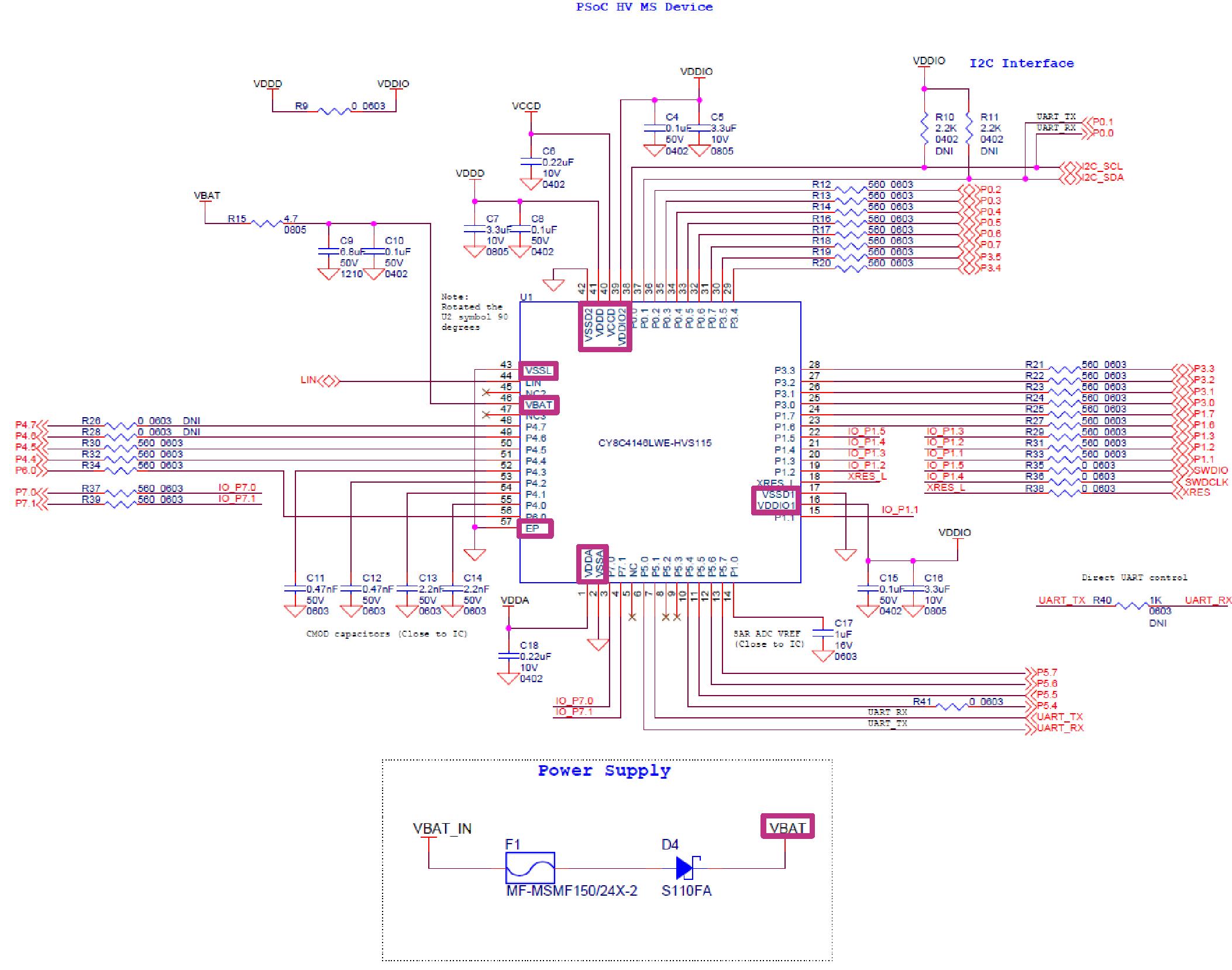
Symbol | Overview | Parameter | ||
|---|---|---|---|---|
Value 1 | Value 2 | Remarks | ||
C4, C15 | Decoupling capacitor for VDDIO domain | 0.1 μF X7R | > 10 V | |
C5, C16 | Decoupling/smoothing capacitor for VDDIO domain | 3.3 μF X7R | > 10 V | |
C6 | Decoupling capacitor for VCCD domain | 0.22 μF X7R | > 6.3 V | |
C7 | Decoupling/smoothing capacitor for VDDD domain | 3.3 μF X7R | > 10 V | |
C8 | Decoupling capacitor for VDDD domain | 0.1 μF X7R | > 10 V | |
C9 | Decoupling/smoothing capacitor for high-voltage domain | 6.8 μF X7S/X7R | >50 V | |
C10 | Decoupling capacitor for high-voltage domain | 0.1 μF X7R | >50 V | |
C18 | Decoupling capacitor for VDDA domain | 0.22 μF X7R | >10 V | |
R15 | High-voltage domain input filter resistance | 4.7 Ω (typical) | >0.2 W | |
D4 | Reverse polarity protection diode | 100 V | 1 A | |
Layout example
shows an example of an HVREG layout.
Figure 8. HVREG layout example
Follow these guidelines for the PCB power supply circuit on the PSOC™ HV MS:
Place the VBAT input capacitors C9 and C10 as close as possible to the VBAT pin. Place capacitor C10 closer to the VBAT pin, followed by capacitor C9. Place the R15 resistor for the input filter next to C9 and draw the layout as linear as possible. If the board has a GND plane, provide a through hole (via) near this capacitor.
Place the VDDA capacitor (C18) as close as possible to the VDDA pin and the VSSA pin to minimize the current loop from VDDA to VSSA. If the board has a GND plane, provide a through hole near the VSSA pin of this capacitor.
Place the VDDD capacitors (C7 and C8) as close as possible to the VDDD pin to minimize the current loop from VDDD to VSSD. Place C8 closest to VDDD, followed by C7. If the board has a GND plane, provide a through hole connecting to the GND plane, near this capacitor.
Place the VDDIO capacitors (C4, C5, C15, and C16 as close as possible to the VDDIO pins to minimize the current loop from VDDIO to VSSD. Place C4 and C15 closest to VDDIO, followed by C5 and C16. If the board has a GND plane, provide a through hole connecting to the GND plane, near this capacitor.
Place the VCCD capacitor (C6) as close as possible to the VCCD pin to minimize the current loop from VCCD to VSSD. If the board has a GND plane, provide a through hole connecting to the GND plane, near this capacitor.
Provide a GND plane on the mounting surface of this IC. To effectively dissipate heat with the 32-QFN, 48- QFN, 56-QFN, or 64-QFN packages, it is recommended to provide a thermal via in the footprint of the thermal pad.
LIN/CXPI PHY
Schematic example
shows an example of LIN schematic;
Table 9
shows an example of external components.
Figure 9. LIN schematic example
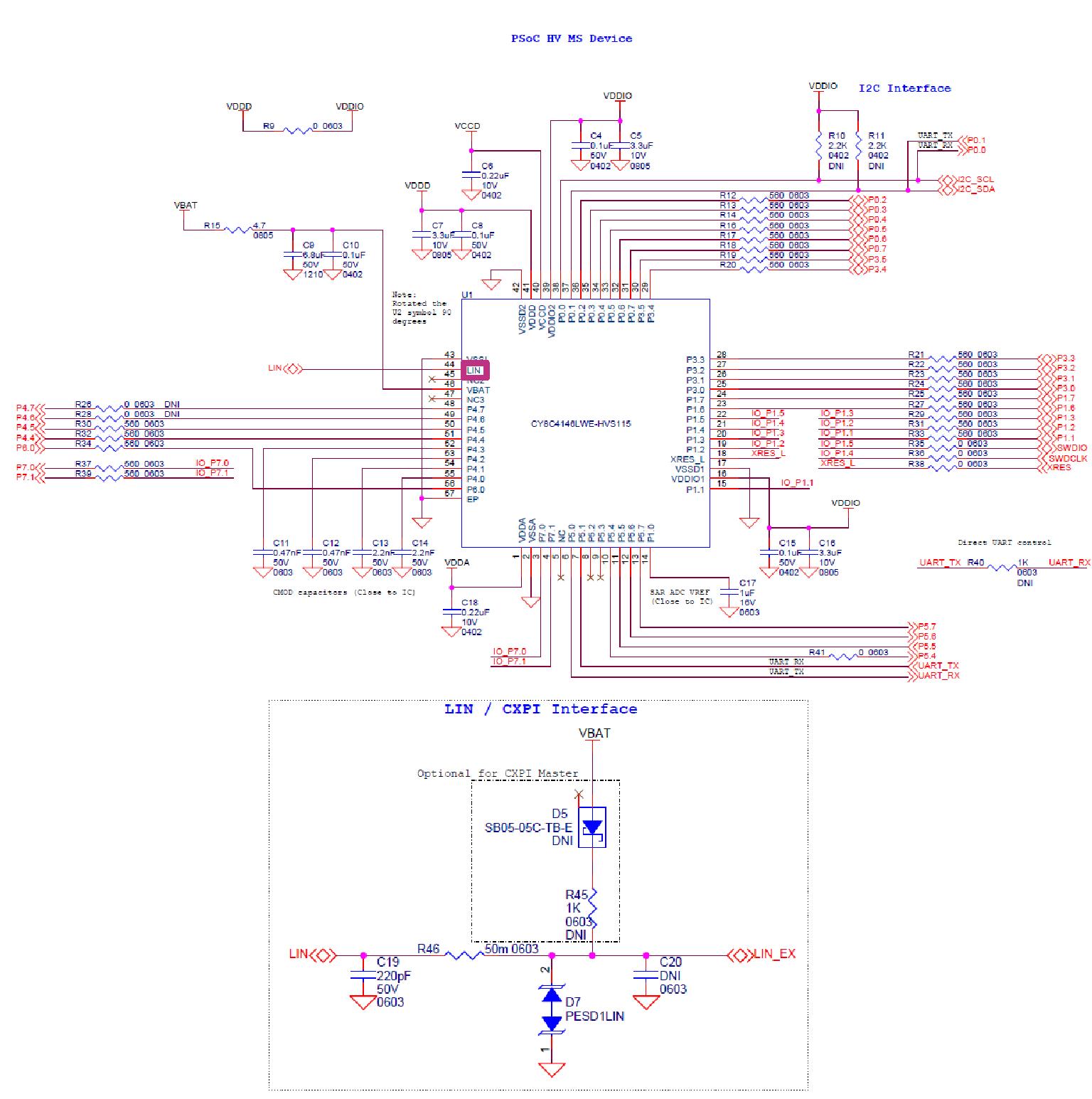
Symbol | Overview | Parameter | ||
|---|---|---|---|---|
Value 1 | Value 2 | Remark | ||
C19 | Decoupling capacitor for the LIN domain | 220 pF C0G | >50 V | |
C20 | Decoupling capacitor for the LIN domain | _ | _ | Optional |
R45 | V BAT pullup resistor | 1 kΩ | >1/8 W | |
R46 | Input filter resistance for the high-voltage domain | 50 mΩ | >1/3 W | |
D5 | Reverse protection diode | 550 mV | 500 mA | |
D7 | Transient voltage suppressor (TVS) diode | Bidirectional | Clamping voltage 44 V | |
Layout example
shows an example of the LIN layout.
Figure 10. LIN layout example
Follow these guidelines for the PCB HVSS circuit:
Place capacitor (C19) near the LIN and VSSL terminals
Place the TVS diode (D7) for ESD protection near the LIN connector
Connect the LIN wiring as straight as possible
Change the optional filter element (R46) as per your application
Place GND vias near the C19 and D7 terminals
Do not connect VSSL to the EP pad
Place a guard under the LIN wiring with a GND layer
Place a guard around LIN with GND
R45 and D5 are optional for CXPI master
ESD protection
Electro-static discharge (ESD) events generate high voltages and high currents depending on the path the charge takes to go to ground. If not properly bypassed, the voltages cause immediate oxide dielectric breakdown, especially in advanced geometry technologies with thin gate oxides, creating a weak spot in the oxide which allows the current flow and localized heating.
Depending on the current flow, this could cause permanent damage. A high current flow can cause overheating and melt the silicon, which results in creating a permanent short or high-leakage sites. High currents can also cause junction or metal failure. In summary, ESD failures can be caused by oxide breakdown, junction burnout, or metallization failure.
The following sections describe the ESD protection mechanism for each HVSS block.
HVREG protection
shows the detailed block diagram for HVREG ESD protection. HVREG includes the cascode ESD transistors and two pads for the VBAT pin. The cascode ESD transistors are used to bypass the charge to ground. Two pads for the VBAT pin reduce the impact by oxide breakdown, junction burnout, or metallization failure due to excess current.
Figure 11. HVREG ESD protection
LIN/CXPI PHY protection
shows the detailed block diagram for LIN/CXPI PHY ESD protection.
LIN/CXPI PHY includes a HVPMOS diode, cascode ESD transistors, and two pads for the LIN and VSSL pins. The cascode ESD transistors are used to bypass the charge to VSSL. The two pads for the LIN and VSSL pins reduce the impact by oxide breakdown, junction burnout, or metallization failure due to excess current.
Figure 12. LIN/CXPI PHY ESD protection
ESD events in an uncontrolled environment
Despite the protection element inside the silicon, ESD events in an uncontrolled environment (users, retail customers, and so on) can be much more damaging. System design must take ESD protection on the PCB into account to prevent ESD events in the uncontrolled environment. This is usually done through techniques such as ESD protection devices (external devices), PCB layout techniques that attempt to control ESD, and appropriate grounding and shielding techniques.
The PSOC™ HV MS device requires sufficient protection to withstand the high-voltage ESD on specific pins. The ESD on LIN/CXPI, and VBAT is rated at ±8 kV, and is required to be protected as shown in
Figure 13
.
Figure 13. External device ESD protection
API details
The following section describes the APIs shown in
Table 4
. See the
SDL_psoc4hvmsXXXk.chm
file in the SDL path below for more information of all PSOC™ HV MS APIs:
C:/<user path>
PSoC_Sample_Driver_Library_x.x.x\docs
Cy_Hvss_Init()
cy_en_hvss_status_t Cy_Hvss_Init(cy_stc_hvss_config_t *config)
Description:
This function configures the HVSS module, which includes RDIV (resistor attenuation) and LIN/CXPI - PHY configuration. This function should be called before using LIN communication functions.
Parameters:
config \ref cy_stc_hvss_config_t
Returns:
CY_HVSS_SUCCESS
– HVSS configuration completed successfully
CY_HVSS_BAD_PARAM
– One or more invalid parameters
CY_HVSS_ERROR
– Error occurred while configuring
Cy_Hvss_DeInit()
cy_en_hvss_status_t Cy_Hvss_DeInit(void)
Description:
This API de-initializes both the LIN module and the RDIV.
Parameters:
None.
Returns:
CY_HVSS_SUCCESS
– HVSS configuration completed successfully
CY_HVSS_BAD_PARAM
– One or more invalid parameters
CY_HVSS_ERROR
– Error occurred while configuring
Cy_Hvss_TrimApply()
cy_en_hvss_status_t Cy_Hvss_TrimApply(cy_stc_hvss_trim_t *trimConfig)
Description:
This function configures the HVSS module trim settings, which includes master, slave, vref and tsd trim from HVREG and slew control trim from LIN.
Parameters:
trimConfig \ref cy_stc_hvss_trim_t
Returns:
CY_HVSS_SUCCESS
– HVSS configuration completed successfully
CY_HVSS_BAD_PARAM
– One or more invalid parameters
CY_HVSS_ERROR
– Error occurred while configuring
Cy_Hvss_Hvreg_SetClampMode()
__STATIC_INLINE void Cy_Hvss_Hvreg_SetClampMode(cy_en_hvss_hvreg_clamp_mode_t mode)
Description:
Set the clamp mode (zender and diode) in HVREG.
Parameters:
\ref cy_en_hvss_hvreg_clamp_mode_t
Returns:
None.
Cy_Hvss_Hvreg_GetClampMode()
__STATIC_INLINE cy_en_hvss_hvreg_clamp_mode_t Cy_Hvss_Hvreg_GetClampMode(void)
Description:
Get the clamp mode (zender and diode) from HVREG.
Parameters:
None.
Returns:
\ref cy_en_hvss_hvreg_clamp_mode_t
Cy_Hvss_Hvreg_SetTsdMode()
__STATIC_INLINE void Cy_Hvss_Hvreg_SetTsdMode(cy_en_hvss_hvreg_tsd_mode_t mode)
Description:
Set the thermal shutdown (TSD) mode in HVREG.
Parameters:
\ref cy_en_hvss_hvreg_tsd_mode_t
Returns:
None.
Cy_Hvss_Hvreg_GetTsdMode()
__STATIC_INLINE cy_en_hvss_hvreg_tsd_mode_t Cy_Hvss_Hvreg_GetTsdMode(void)
Description:
Get the thermal shutdown (TSD) mode from HVREG.
Parameters:
None.
Returns:
\ref cy_en_hvss_hvreg_tsd_mode_t
Cy_Hvss_Hvreg_EnableVbatDivider()
__STATIC_INLINE void Cy_Hvss_Hvreg_EnableVbatDivider(void)
Description:
Enable VBAT voltage divider in HVREG.
Parameters:
None.
Returns:
None.
Cy_Hvss_Hvreg_DisableVbatDivider()
__STATIC_INLINE void Cy_Hvss_Hvreg_DisableVbatDivider(void)
Description:
Disable VBAT voltage divider in HVREG.
Parameters:
None.
Returns:
None.
Cy_Hvss_Hvreg_GetStatus()
__STATIC_INLINE uint8_t Cy_Hvss_Hvreg_GetStatus(void)
Description:
Get status of regulator of HVSS.
Parameters:
None.
Returns:
PWR_GOOD
– Status bit.
Cy_Hvss_Hvreg_SetBistMasterAdft()
__STATIC_INLINE void Cy_Hvss_Hvreg_SetBistMasterAdft(cy_en_hvss_hvreg_bist_master_type_t adft)
Description:
Set the master ADFT switches in HVREG.
Parameters:
adft \ref cy_en_hvss_hvreg_bist_master_type_t
Returns:
None.
Cy_Hvss_Hvreg_GetBistMasterAdft()
__STATIC_INLINE cy_en_hvss_hvreg_bist_master_type_t Cy_Hvss_Hvreg_GetBistMasterAdft(void)
Description:
Get the master ADFT switches from HVREG.
Parameters:
None.
Returns:
\ref cy_en_hvss_hvreg_bist_master_type_t
Cy_Hvss_Hvreg_EnableDdft()
__STATIC_INLINE void Cy_Hvss_Hvreg_EnableDdft(void)
Description:
Enable HVREG DDFT outputs to DDFT interface PG on ddft0.
Parameters:
None.
Returns:
None.
Cy_Hvss_Hvreg_DisableDdft()
__STATIC_INLINE void Cy_Hvss_Hvreg_DisableDdft(void)
Description:
Disable HVREG DDFT outputs to DDFT interface.
Parameters:
None.
Returns:
None.
Cy_Hvss_Hvreg_DisableDdft()
__STATIC_INLINE void Cy_Hvss_Hvreg_DisableDdft(void)
Description:
Disable HVREG DDFT outputs to DDFT interface.
Parameters:
None.
Returns:
None.
Cy_Hvss_Hvreg_EnableBurnMode()
__STATIC_INLINE void Cy_Hvss_Hvreg_EnableBurnMode(void)
Description:
Enable burn-in test mode with Vccd(1.8V) domain in HVREG.
Parameters:
None.
Returns:
None.
Cy_Hvss_Hvreg_DisableBurnMode()
__STATIC_INLINE void Cy_Hvss_Hvreg_DisableBurnMode(void)
Description:
Disable burn-in test mode with Vccd(1.8V) domain in HVREG.
Parameters:
None.
Returns:
None.
Cy_Hvss_LinPhy_SetRxdPin()
__STATIC_INLINE void Cy_Hvss_LinPhy_SetRxdPin(uint8_t status)
Description:
Set status of LIN/CXPI -PHY RxD pin.
Parameters:
status lin
– RxD pin status (HIGH or LOW).
Returns:
None.
Cy_Hvss_LinPhy_GetRxdPin()
__STATIC_INLINE uint8_t Cy_Hvss_LinPhy_GetRxdPin(void)
Description:
Get status of LIN/CXPI -PHY, will give current status of LIN RxD pin.
Parameters:
None.
Returns:
uint8_t
Cy_Hvss_LinPhy_EnableWakeupTimer()
__STATIC_INLINE void Cy_Hvss_LinPhy_EnableWakeupTimer(void)
Description:
Enable the LIN/CXPI -PHY wake-up timer, required LIN compatibility in DS mode.
Parameters:
None.
Returns:
None.
Cy_Hvss_LinPhy_DisableWakeupTimer()
__STATIC_INLINE void Cy_Hvss_LinPhy_DisableWakeupTimer(void)
Description:
Disable the LIN/CXPI -PHY wake-up timer.
Parameters:
None.
Returns:
None.
Cy_Hvss_LinPhy_GetWakeupTimerStatus()
__STATIC_INLINE uint16_t Cy_Hvss_LinPhy_GetWakeupTimerStatus(void)
Description:
Get status of LIN/CXPI -PHY wakeup timer, will give timer count if running.
Parameters:
None.
Returns:
uint16_t
Cy_Hvss_LinPhy_EnableFaultTimer()
__STATIC_INLINE void Cy_Hvss_LinPhy_EnableFaultTimer(void)
Description:
Enable the LIN/CXPI -PHY fault timer, required LIN compatibility in DS mode.
Parameters:
None.
Returns:
None.
Cy_Hvss_LinPhy_DisableFaultTimer()
__STATIC_INLINE void Cy_Hvss_LinPhy_DisableFaultTimer(void)
Description:
Disable the LIN/CXPI -PHY fault timer.
Parameters:
None.
Returns:
None.
Cy_Hvss_LinPhy_GetFaultTimerStatus()
__STATIC_INLINE uint16_t Cy_Hvss_LinPhy_GetFaultTimerStatus(void)
Description:
Get status of LIN/CXPI -PHY fault timer, will give timer count if running.
Parameters:
None.
Returns:
uint16_t
Cy_Hvss_LinPhy_SetPhyMode()
__STATIC_INLINE void Cy_Hvss_LinPhy_SetPhyMode(cy_en_hvss_lin_phy_mode_type_t mode)
Description:
Set mode of LIN/CXPI -PHY.
Parameters:
mode /ref cy_en_hvss_lin_phy_mode_type_t
Returns:
None
Cy_Hvss_LinPhy_GetPhyMode()
__STATIC_INLINE cy_en_hvss_lin_phy_mode_type_t Cy_Hvss_LinPhy_GetPhyMode(void)
Description:
Get current mode of LIN/CXPI -PHY.
Parameters:
None.
Returns:
/ref cy_en_hvss_lin_phy_mode_type_t
Cy_Hvss_LinPhy_
SetPhySlRound()
__STATIC_INLINE void Cy_Hvss_LinPhy_SetPhySlRound(cy_en_hvss_lin_phy_emi_type_t mode)
Description:
Set rf_detect value of LIN/CXPI -PHY, for lower EMI.
Parameters:
mode /ref cy_en_hvss_LinPhy_emi_type_t
Returns:
None.
Cy_Hvss_LinPhy_GetPhySlRound()
__STATIC_INLINE cy_en_hvss_lin_phy_emi_type_t Cy_Hvss_LinPhy_GetPhySlRound(void)
Description:
Get rf_detect mode of LIN/CXPI -PHY.
Parameters:
None.
Returns:
/ref cy_en_hvss_LinPhy_emi_type_t
Cy_Hvss_LinPhy_SetPhyInterface()
__STATIC_INLINE void Cy_Hvss_LinPhy_SetAltPhyInterface(cy_en_hvss_alt_phy_interface_type_t mode)
Description:
Set internal or GPIO connection of LIN/CXPI -PHY through HSIOM.
Parameters:
mode /ref cy_en_hvss_LinPhy_interface_type_t
Returns:
None.
Cy_Hvss_LinPhy_GetPhyInterface()
__STATIC_INLINE cy_en_hvss_alt_phy_interface_type_t Cy_Hvss_LinPhy_GetAltPhyInterface(void)
Description:
Get connection interface of LIN/CXPI -PHY, through internal or GPIO.
Parameters:
None.
Returns:
/ref cy_en_hvss_LinPhy_interface_type_t
Cy_Hvss_LinPhy_SelectPhyInterfaceType()
__STATIC_INLINE void Cy_Hvss_LinPhy_SelectPhyInterfaceType(cy_en_hvss_phy_interface_type_t phyType)
Description:
Set LIN or CXPI PHY type.
Parameters:
phyType /ref cy_en_hvss_phy_interface_type_t
Returns:
None.
Cy_Hvss_LinPhy_GetPhyInterfaceType()
__STATIC_INLINE cy_en_hvss_phy_interface_type_t Cy_Hvss_LinPhy_GetPhyInterfaceType(void)
Description:
Get PHY interface type.
Parameters:
None.
Returns:
/ref cy_en_hvss_phy_interface_type_t
Cy_Hvss_LinPhy_EnablePhy()
__STATIC_INLINE void Cy_Hvss_LinPhy_EnablePhy(void)
Description:
Enable the LIN/CXPI -PHY.
Parameters:
None.
Returns:
None.
Cy_Hvss_LinPhy_DisablePhy()
__STATIC_INLINE void Cy_Hvss_LinPhy_DisablePhy(void)
Description:
Disable the LIN/CXPI -PHY.
Parameters:
None.
Returns:
None.
Cy_Hvss_LinPhy_GetPhyStatus()
__STATIC_INLINE uint8_t Cy_Hvss_LinPhy_GetPhyStatus(void)
Description:
Get status of LIN/CXPI -PHY, 1- enabled and 0 - reset (RxD pin is HighZ).
Parameters:
None.
Returns: Uint8_t
Cy_Hvss_LinPhy_ClearInterrupt()
__STATIC_INLINE void Cy_Hvss_LinPhy_ClearInterrupt(uint32_t interrupt)
Description:
Clears interrupt from the LIN_INTR register.
Parameters:
interrupt
: interrupt mask for the interrupt.
Returns:
None.
Cy_Hvss_LinPhy_SetInterrupt()
__STATIC_INLINE void Cy_Hvss_LinPhy_SetInterrupt(uint32_t interrupt)
Description:
Sets interrupt in the LIN_INTR register.
Parameters:
interrupt: interrupt mask for the interrupt.
Returns:
None.
Cy_Hvss_LinPhy_GetInterruptMask()
__STATIC_INLINE uint32_t Cy_Hvss_LinPhy_GetInterruptMask(void)
Description:
Return the interrupt mask from the LIN_INTR_MASK register
Parameters:
None.
Returns:
The interrupt bit mask
Cy_Hvss_LinPhy_SetInterruptMask()
__STATIC_INLINE void Cy_Hvss_LinPhy_SetInterruptMask(uint32_t interrupt)
Description:
Sets the interrupt mask in the LIN_INTR_MASK register.
Parameters:
interrupt
: interrupt mask for the interrupt.
Returns:
None.
Cy_Hvss_LinPhy_GetInterruptStatusMasked()
__STATIC_INLINE uint32_t Cy_Hvss_LinPhy_GetInterruptStatusMasked(void)
Description:
Return the masked status from LIN_INTR_MASKED register.
Parameters:
None.
Returns:
The interrupt bit mask(s).
Cy_Hvss_LinPhy_SetWakeupInterruptMask()
__STATIC_INLINE void Cy_Hvss_LinPhy_SetWakeupInterruptMask(void)
Description:
Sets wakeup interrupt status masked in LIN_INTR_MASK register.
Parameters:
None.
Returns:
None
Cy_Hvss_LinPhy_ClearWakeupInterruptMask()
__STATIC_INLINE void Cy_Hvss_LinPhy_ClearWakeupInterruptMask(void)
Description:
Clears wakeup interrupt status masked in LIN_INTR_MASK register.
Parameters:
None.
Returns:
None
Cy_Hvss_LinPhy_SetFaultInterruptMask()
__STATIC_INLINE void Cy_Hvss_LinPhy_SetFaultInterruptMask(void)
Description:
Sets fault interrupt status masked in LIN_INTR_MASK register.
Parameters:
None.
Returns:
None
Cy_Hvss_LinPhy_ClearFaultInterruptMask()
__STATIC_INLINE void Cy_Hvss_LinPhy_ClearFaultInterruptMask(void)
Description:
Clears fault interrupt status masked in LIN_INTR_MASK register.
Parameters:
None.
Returns:
None
Cy_Hvss_LinPhy_SetTsdInterruptMask()
__STATIC_INLINE void Cy_Hvss_LinPhy_SetTsdInterruptMask(void)
Description:
Sets HVREG TSD interrupt status masked in LIN_INTR_MASK register.
Parameters:
None.
Returns:
None
Cy_Hvss_LinPhy_ClearTsdInterruptMask()
__STATIC_INLINE void Cy_Hvss_LinPhy_ClearTsdInterruptMask(void)
Description:
Clears HVREG TSD interrupt status masked in LIN_INTR_MASK register.
Parameters:
None.
Returns:
None.
Summary
This application note provided details regarding high-voltage subsystem of PSOC™ HV MS. By using the high voltage subsystem, automotive batteries can be connected directly and can be achieved with a small number of external components for several automotive HMI, body, and powertrain applications. Infineon provides evaluation boards and a wealth of sample software to help you get started with PSOC™ HV MS family. To get access to the evaluation board, contact your sales representative or
Infineon technical support
.
Acronyms
Acronym | Expansion |
|---|---|
A/D converter | analog to digital converter |
ADC | analog to digital converter |
AHB | advanced high-performance bus |
API | application programming interface |
BOD | brown-out detectors |
CPU | central processing unit |
CPUSS | CPU subsystem |
CXPI | clock extension peripheral interface |
DAP | debug access port |
DC | direct current |
DMA | direct memory access |
DMAC | DMA controller |
DW | data wire |
ECC | error correction code (safety) |
ECU | electronic control unit |
EM | electro-magnetic |
EMI | electro-magnetic interference |
ESD | electro-static discharge |
GPIO | general purpose I/O |
HMI | human machine interface |
HSIOM | high-speed I/O matrix |
HVPMOS | high-voltage p-channel metal-oxide semiconductor |
HVREG | high-voltage regulator |
HVSS | high-voltage subsystem |
I/O | input or output |
IOSS | I/O subsystem |
IRC | interrupt controller |
IRQ | interrupt request |
ISO | international organization for standardization |
ISR | interrupt service routine |
LIN | local interconnect network |
MCU | microcontroller unit |
MPU | memory protection unit |
MS | mixed signal |
MSC | multi-sense converter |
NMI | non-maskable interrupt |
PCB | printed circuit board |
PG | power good |
PHY | physical interface transceiver |
POR | power on reset |
PWM | pulse width modulation |
RAM | random access memory |
RDIV | resistor attenuator control |
RF | radio frequency |
ROM | read-only memory |
SAR | successive approximation register |
SCB | serial communication block |
SDL | sample driver library |
SPI | serial peripheral interface |
SRAM | static RAM |
SRSS | system resource subsystem |
TCPWM | timer, counter and PWM |
TRM | technical reference manual |
TSD | thermal shutdown detector |
TVS | transient voltage suppressor |
UART | universal asynchronous receiver/transmitter |
VBAT | voltage battery |
VDIVIDER | voltage divider |
WDT | watchdog timer |
References
The following documents related to the PSOC™ HV MS family series can be obtained by contacting
Infineon technical support
.
AN234115 – Getting started with PSOC™ HV MS family
AN234116 – Hardware design guide for PSOC™ HV MS family
PSOC™ HV mixed signal datasheet
PSOC™ HV MS architecture technical reference manual (TRM)
PSOC™ HV MS registers technical reference manual (TRM)
PSOC™ HV MS Evaluation Board user guide
PSOC™ HV MS Sample Driver Library
Revision history
Document revision | Date | Description of changes |
|---|---|---|
V1.0 | 2023-11-30 | Initial release |
V1.1 | 2025-06-26 | Template update Updated PSoC™ to PSOC™ |
Trademarks
PSOC™, formerly known as PSoC™, is a trademark of Infineon Technologies. Any references to PSoC™ in this document or others shall be deemed to refer to PSOC™.