Button tab
The Button tab is used to design an inductive sensing coil and its parameters for the preferred application requirements and generate a *.dxf file.
Commands
-
Restore Defaults - Restores parameters values on the current tab to their default values.
-
Copy All - Click this button to copy the list of input and output parameters to the system clipboard as plain text.
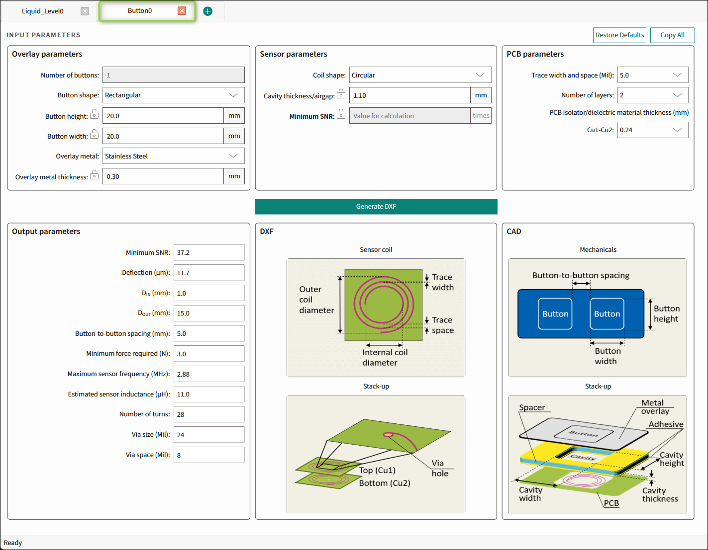
Input parameters
The Input parameters include Overlay, Sensor, and PCB parameters.
The first output parameter will always be the same parameter, which is locked ![]() in the Input parameters section. Lock the relevant parameter by double-clicking its unlocked icon
in the Input parameters section. Lock the relevant parameter by double-clicking its unlocked icon ![]() . Only one parameter can be locked at a time.
. Only one parameter can be locked at a time.
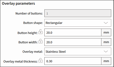
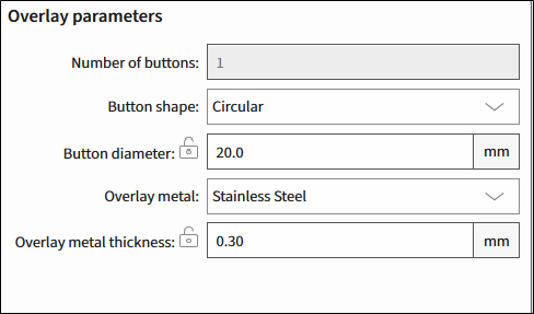
Overlay parameters
| Rectangular | Circular |
|---|---|
 |  |
-
Number of buttons - The number of buttons in the specified widget. Default – 1.
-
Button shape - Rectangular, Circular. Default – Rectangular.
-
Button height (mm) - Visible only for a rectangular button. For Cavity thickness/airgap, the dimensions are the same. The range is 8-28, default – 20.
-
Button width (mm) - Visible only for a rectangular button. For Cavity height/width, the dimensions are the same. The range is 8-28, default – 20.
-
Button diameter (mm) - Visible only for a circular button. The range is 8-28, default – 20.
-
Overlay metal 1 – Stainless Steel, Aluminum. Default – Stainless Steel.
-
Overlay metal thickness (mm) - The thickness of the specified overlay. The range is 0.2-0.5, default – 0.30.
-
Stainless Steel – The range is 0.2-0.5, default – 0.30.
-
Aluminum – The range is 0.25-0.5, default – 0.30.
-
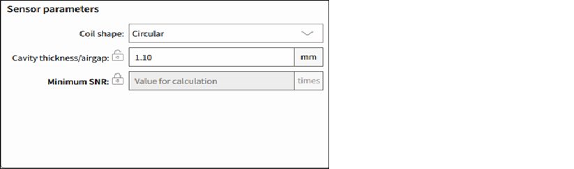
Sensor parameters
-
Coil shape 2 – Circular, Rectangular, Hexagonal, Oval. Default – Circular.
-
Cavity thickness/airgap (mm) – The gap between the overlay and the sensor coil. The range is 0.3-7. Default – 1.10.
-
Minimum SNR (times) – The minimum SNR required for the sensor optimum performance. The range is 1-40.
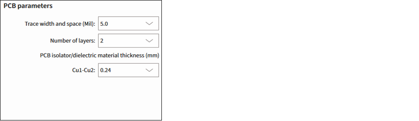
PCB parameters
-
Trace width and space (Mil) - The minimum sensor PCB trace width for generating output parameters. Select from: 3.5, 4.0, 5.0, or 7.0. Default – 5.
-
Number of layers - The number of Cu layers. Select from: 1, 2 or 4. Default – 2.
-
PCB isolator/dielectric material thickness (mm) - Enabled for more than 1 layer. The thickness of PCB Isolator or dielectric material used between Cu layers.
- For 2 layers, Cu1-Cu2, select from: 0.24, 0.4, 1.0, 1.2. Default – 0.24.
- For 4 layers, the spaces between the layers are fixed: 0.24 – 1.0 – 0.24.
Generate DXF
Click this button to generate a *.dxf file of the calculated liquid level sensor to a specified file location.
![]()
This button is disabled if the calculated value is beyond the allowed range and the first field of the Output parameters indicates that.
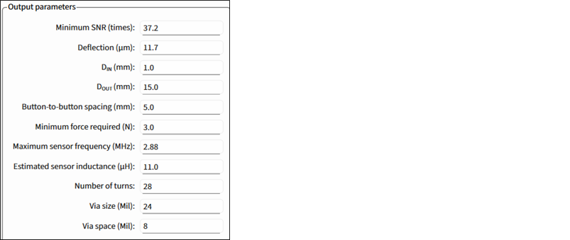
Output parameters
The first output parameter will always be the same parameter, which is locked ![]() in the Input parameters section. Lock the relevant parameter by double-clicking its unlock
in the Input parameters section. Lock the relevant parameter by double-clicking its unlock ![]() icon .
icon .
Only one parameter can be locked at a time.
-
Button height and width, Button diameter, Minimum SNR (times), Overlay metal thickness, and Cavity thickness/airgap - The calculated value of a specified parameter.
-
Deflection (µm) - The overlay deflection for the minimum force applied to trigger the sensor to achieve the calculated or specified SNR.
-
D IN ** (mm)** - The sensor-coil inner diameter/diagonal.
-
D OUT (mm) - The sensor-coil outer diameter/diagonal. Always – 75 % of the referred button size.
-
Button-to-button spacing (mm) - The minimum spacing between buttons.
-
Minimum force required (N) - The minimum sensor-activation force to achieve the calculated or specified SNR. Always – 3 N.
-
Maximum sensor frequency (MHz) - The maximum sensor-drive frequency.
-
Estimated sensor inductance (µH) - The estimated effective sensor coil inductance. The estimate is based on the number of coil turns, trace width, PCB layers, PCB layers spacing.
-
Number of turns - The number of coil turns per each layer.
-
Via size (Mil) - The diameter of the through-hole pad in the multi-layer PCB.
-
Via space (Mil) - Spacing between through-hole pads and coil wire in the multi-layer PCB.
Illustration of DXF design
Displays the calculated structure of a designed sensor array.
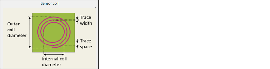
Sensor coil
The illustrative image of a sensor coil.
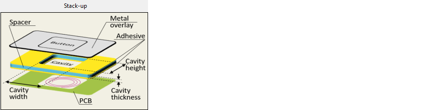
Stack-up
The illustrative image of a DXF Stack-up.
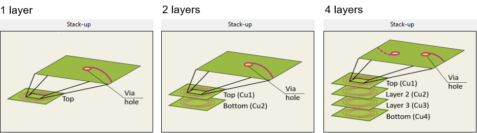
Illustration of CAD design
Displays the calculated mechanical structure of a designed button.
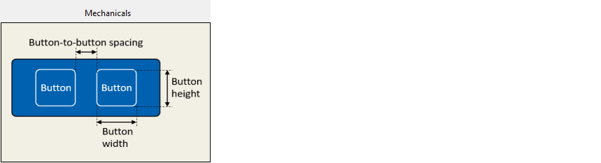
Mechanicals
The illustrative image of the buttons' placement.
Stack-up
The illustrative image of the CAD stack-up.