PSOC™ Control C3 - PSC3P5xD, PSC3M5xD
Arm®
Cortex®-M33 32-bit MCU+FPU+DSP, 180 MHz,
up to 256 KB Flash/64 KB SRAM, Real-time Control
PSOC™ Control package image
Features
High-performance, low-power 32-bit single-core Arm® Cortex® M33-based microcontroller with digital signal processor (DSP), floating-point unit (FPU), and state-of-the-art security features
High-performance, programmable analog subsystem (HPPASS):
12-bit,12-MspsSAR ADC with parallel idle sampling of up to 16 analog channels
Five comparators with <10 ns built-in 10-bit DAC and slope generator
Real-time control peripherals:
Coordinate rotation digital computer (CORDIC)
16 x 16-bit and 4 x 32 bit timer/counter pulse-width modulator (TCPWM) supporting <80 ps high-resolution pulse-width modulator (HRPWM)
Enhanced routing flexibility with a combinatorial trigger multiplexing unit
Communication interfaces: Up to six SCB and two CAN FD (one supporting 8 Mbps)
256 KB read-while-write flash with ECC support
Low-power operation modes down to 300 nA: Sleep, Deep Sleep (three modes) and Hibernate
Up to 50 GPIOs with programmable drive modes, strengths, and slew rates; up to 28 pins support Smart I/O programmable logic and up to 16 dedicated analog pins
Security: PSA L2 certified; configurable flash partitioning and protection
Safety: Class B and SIL 2 compliant safety test libraries are available
Power supply range: 1.71 V to 3.6 V
Ambient temperature range: -40°C to 105°C Ta
Packages: VQFN-48, E-LQFP-48, VQFN-64, E-LQFP-64 , E-LQFP-80
Potential applications
Motor control in power tools, home appliances, industrial drives, light electric vehicles, robotics, and drones
Digital power control in switched mode power supply (SMPS) and PFC applications for LED lighting, EV chargers, solar inverters, servers, and PC power supplies
Wide bandgap technologies (e.g., SiC and GaN) based motor control and power conversion applications
Description
The
PSC3P5xD
and
PSC3M5xD
devices are based on the Arm® Cortex®-M33 running up to
180 MHz
with DSP and FPU capability. In addition to the CPU subsystem, the devices contain advanced real-time control peripherals, such as high-performance programmable analog subsystem, comparators, advanced timers with high-resolution capability, up to six SCBs and two CAN FDs for communication. The devices support one Active and five low-power modes for managing and reducing the power consumption depending on application requirements.
Introduction
The
PSC3P5xD
and
PSC3M5xD
devices are part of the
PSOC™ Control C3
MCU family designed for real-time control, enhanced sensing, secure, and low-power operations. Some target applications for these microcontrollers are:
Industrial motor-controllers
Power-stage converters
Home appliances
Automation devices
Low-power sensors
A detailed block diagram of the MCU is shown in
Figure 1
.
Figure 1.
Functional block diagram
Device identification and revisions
Family ID = 0x118(12‑bit); Si ID range = EE40- EE7F; Major‑minor rev ID = 0x1, 0x1
Detailed features
This device has the following features:
CPU subsystem
Arm® Cortex®-M33 running up to 180 MHz
Digital signal processor (DSP), floating-point unit (FPU), memory protection unit (MPU), 16 KB I-cache
Two direct memory access (DMA) controllers with 16 channels each
Security
Platform security architecture level 2 (PSA L2) certified
Step-wise authentication of execution images until the control is handed over to the user code
Secure execution of code in the execute-only mode for protected routines
Image authentication and integrity check
TrustZone framework that establishes an isolated device root of trust (RoT) for trust attestation and software management
Memory
On-chip flash with ECC support
Up to 256-KB flash with read while write (RWW) capability, 64 KB ROM for boot code, and bootloader functions
Built-in device firmware upgrade (DFU) support in boot ROM via serial interface (UART/I2C/SPI)
SRAM with ECC support
64 KB full SRAM available in Deep Sleep
SRAM data path is protected with a hardware mechanism (ECC) for soft error detection and correction
Clocking subsystem
8 MHz IMO with Deep Sleep operation offering ±2% accuracy
48 MHz internal high-frequency oscillator (IHO) offering ±1% accuracy
32 kHz internal low frequency oscillator (ILO) offering ±10% accuracy
4 to 35 MHz external crystal oscillator (ECO) support
32.768 kHz external watch crystal oscillator (WCO) usable for real-time clock (RTC)
External clock (EXTCLK): Maximum frequency 80 MHz
One frequency lock loop (FLL) with 24-100 MHz output range
Two digital phase-locked loops, DPLL#0 and DPLL#1, with 25-250 MHz output range
Low power (1.71 V to 3.6 V) operation
Six power modes (Active, Sleep, Deep Sleep, Deep Sleep-RAM, Deep Sleep-OFF, and Hibernate) for fine-grained power management
Deep Sleep mode current of 11 µA at 3.3-V external supply using an internal voltage regulator with 64-KB SRAM retention, LPComp, and Deep Sleep SCB
Hibernate mode current with RTC and LPComp of up to 1000 nA
Communication peripherals
Serial communication blocks (SCBs)
Up to six independent run-time-reconfigurable SCBs; each is software-configurable as I2C, SPI, or UART in master or slave mode
One SCB also supports Deep Sleep operation and wake-up from Deep Sleep in I2C slave and SPI slave modes
One SCB has fast SPI support of up to 50 MHz
SCB supports single-wire half-duplex mode for UART
CAN FD
Up to two CAN FD channels with a single instance with operation of up to 8 Mbps
High-performance, programmable analog subsystem (HPPASS)
Analog-to-digital converter (ADC)
One 12-bit, 12-Msps SAR ADC
Up to 16 dedicated analog pads, connected to up to 16 parallel sample stages
Two additional GPIOs can be used as analog inputs
Up to 16 sample/hold (S/H) circuits in SAR ADC connected to pins directly or through AMUX
One S/H circuit in SAR ADC is internally connected to analog references and a temperature sensor
Configurable input gain of 1, 3, 6, and 12 on all 16 S/H circuits
Digital comparator at the output to compare the ADC result against programmed boundary values
Digital comparator outputs can be connected to timer/counter pulse-width modulator (TCPWM) (low latency between the modules)
Analog comparators
Five Active comparators without Deep Sleep functionality, each with a 10-bit DAC to generate the comparator reference
Each comparator supports an external reference/threshold through pins
Active comparator can be used with the built-in DAC in Hysteresis mode
Two additional comparators in LPComp are available in Active/Deep Sleep/Hibernate modes
Comparator outputs can be brought to pins for control loop applications
Comparator outputs can be connected to TCPWM (low latency between the modules)
Logical OR of multiple comparator trigger outputs connected as an input trigger to TCPWM via trigger MUX
Real-time control peripherals
Coordinate rotation digital computer (CORDIC)
Supports all CORDIC operating modes for solving circular (trigonometric), hyperbolic functions, and integrated independent lookup tables to accelerate calculation
Timer/counter pulse-width modulator (TCPWM)
Sixteen 16-bit TCPWM channels
Four 32-bit TCPWM channels supporting high-resolution PWM generation (HRPWM) for PWM outputs
Center-aligned, edge, and pseudorandom modes
Comparator-based triggering of kill signals
Shadow update of duty, period, dead-time, output signal polarity, and dithering (pseudorandom mode)
Multichannel control: In a group of eight TCPWM channels, one channel within a group can trigger another channel
Ability to logically combine the outputs of multiple channels through Smart I/O
Dedicated output triggers mux in a group to allow flexibility to the PWM channel as a trigger and/or gate signals to the HPPASS
Hall sensor interface with autonomous BLDC block commutation support
Quadrature encoder interface to decode motor speed and rotor position
HRPWM feature for period, duty, and dead-time insertion with a typical resolution of less than 80 ps
I/O subsystem
Programmable GPIO pins
Up to 66 functional pins (50 digital GPIOs; 2 out of 50 GPIOs can be used for analog inputs + 16 dedicated analog-only inputs)
Programmable drive modes, strengths, and slew rates
Programmable digital
Up to seven Smart I/O capable ports (28 I/Os, 56 LUTs) enable Boolean operations on I/O signals
Cryptography
Cryptography accelerator
Hardware acceleration for symmetric (AES-128) and asymmetric cryptographic algorithms (RSA and elliptic curve cryptography (ECC)) supported by vector unit (VU) and hash functions (SHA-256)
True random number generator (TRNG) function
Chip-level functional description
Power
The device offers multiple features for managing and reducing power draw. Multiple power modes include Active, Sleep, Deep Sleep, and Hibernate. Deep Sleep has three variations based on retention of SRAM.
The power control block provides assurance that voltage levels meet the requirements of the respective modes. It can:
Delay mode entry (for example, at power-on reset (POR)) until voltage levels are as required for proper functioning
Detect operation below safe power supply levels:
Generates interrupts for low-voltage detection (LVD)
Generates reset for brownout detection (BOD)
The device operates using a single regulated VDDD supply within the range of 1.71 V to 3.6 V. In addition, there is an optional VBACKUP supply that can be used, which has a range of 1.4 V to 3.6 V. A linear regulator powers the core logic at four voltage levels:
0.9 V, 1.0 V, 1.1 V, and 1.2 V
. Voltage level switching is implemented by writing to the power control registers. The voltage for the core logic can be set based on the application's performance and power requirements; (see
Power modes
). With clock gating at peripheral and bus levels, this permits fine-grained optimization of energy usage.
Typically, the backup domain requires an input voltage of 1.4 V to 3.6 V, which can be provided by connecting a backup battery or a super capacitor to the VBACKUP pin. The internal backup switch automatically selects between VDDD and VBACKUP (when VDDD is no longer available) for powering the backup domain peripherals like RTC, WCO, ILO, and Backup registers. Some I/O cells are powered from the VBACKUP supply before the internal backup switch. If the application does not require a dedicated backup source, VBACKUP can be connected to VDDD externally to ensure that the I/O cells powered by VBACKUP are functional.
The device has multiple VDDIO pins that are used to power the I/O cells except the backup domain I/O cells. VDDIO can either be connected to the same supply as VDDD or an independent supply voltage within the valid operating range. This provides more flexibility in terms of choosing the logic level for the port pins powered using different VDDIO supplies. The VDDIO supply can be switched off if the port I/Os are not used. Switching off the VDDIO supply is only allowed in Active or Deep Sleep mode. VDDIO should not be switched off when the device is in Hibernate mode. Refer to the
gxg1730181873132.html#mfy1698739677971
section for information about the VBACKUP or VDDIO supply used for powering the port I/O cells.
Power connections
The following power system diagrams show typical connections for the power pins for all the supported packages. In these diagrams, the package pin is shown with the pin name, for example, "VDD;
9
".
There is no dependency on power supply sequencing.
Figure 2.
LQFP-80 package power connections
Figure 3.
LQFP-64/QFN-64 package power connection
Figure 4.
LQFP-48/QFN-48 package power connections
Power domains
The device has independent power domains, allowing the domain power to be enabled/disabled depending on the power mode.
A diagram of the power connections and routing is shown in
Figure 4
:
Figure 5.
Power distribution and domains
Power modes
The device can operate in five power modes. These power modes are intended to minimize the average power consumption in an application.
Power modes supported are:
Active/Sleep:
All peripherals are powered. The CPU is either active and executing the code or can be put in sleep (clock gated). Any interrupt can wake up the CPU within one CPU clock cycle to resume operation. In Active/Sleep mode, the core voltage can be set to any of the four values. This impacts both power consumption and maximum clock frequency for CPU and peripherals. The following power profiles are supported in Active/Sleep mode:
ULP (Ultra Low Power): 0.9 V core voltage with 50 MHz CPU frequency
MF (Medium Frequency): 1.0 V core voltage with 70 MHz CPU frequency
LP (Low Power): 1.1 V core voltage with
150 MHz
CPU frequency
OD (Overdrive): 1.2 V core voltage with 180 MHz CPU frequency
Deep Sleep:
The CPU is in retention mode. RAM content is also retained. Only Deep Sleep capable peripherals can wake up the system. Once awake, the operation resumes
Deep Sleep-RAM:
The CPU is turned off. 64 KB of SRAM is retained for a warm boot after wake-up. Only Deep Sleep-capable peripherals are operational if enabled and are capable of waking up the system
Deep Sleep-OFF
Same as Deep Sleep RAM except RAM is also turned off. The wake-up action is reset or cold boot
Hibernate:
All peripherals except LPComp and backup domain peripherals such as RTC is turned off. All clocks except the backup domain clock and all internal regulators are turned off. This results in asynchronous operation of the LPComp. The system is reset when it exits the Hibernate mode
Power mode transitions
The device supports Arm® standard power modes; see the
Power modes
section for details.
Table 1
lists the parameters for supported power modes:
Active/Sleep | Deep Sleep | Deep Sleep-RAM | Deep Sleep-OFF | Hibernate | Off | |
|---|---|---|---|---|---|---|
Parameters | ||||||
Wake source 1 | Any interrupt | DS peripherals | DS peripherals | DS peripherals | RTC/HIB peripherals | Power on |
Wake action | Resume | Resume | Warm boot | Reset/cold boot | Reset | Reset |
Wake time | One CPU cycle | <20 µs | Deep Sleep + warm boot | Deep Sleep + cold boot | POR + cold boot < 1 ms | |
Resources | ||||||
ECO | On/Off | Off | Off | Off | Off | Off |
IHO | On | Off | Off | Off | Off | Off |
IMO | On | On/Off | Off | Off | Off | Off |
ILO | On/Off | On/Off | On/Off | On/Off | On/Off | Off |
WCO | On/Off | On/Off | On/Off | On/Off | On/Off | Off |
CPU | On/Sleep | Retention | Off | Off | Off | Off |
SRAM | On | On | On/Off | Off | Off | Off |
Power block support
shows the available operational states for the major blocks in this device. Note that the operational states possible in low-power modes are generally limited in functionality and parametric performance as compared to their capabilities in the Active power mode. Additionally, blocks that do not support low-power modes such as Deep Sleep and Hibernate cannot wake up the CPU from these power modes. See
Power modes
for details.
Block | Power mode | ||||
|---|---|---|---|---|---|
Active | Sleep | Deep Sleep | Hibernate | Backup | |
CPUSS | |||||
CPU | Y | N | N | N | N |
NVIC | Y | Y | N | N | N |
WIC | Y | Y | Y | Y | N |
FLASH | Y | Y | N | N | N |
SRAM | Y | Y | Y | N | N |
DMA | Y | Y | N | N | N |
Programmable digital | |||||
SMART I/O | Y | Y | Y | N | N |
Fixed function digital | |||||
TCPWM | Y | Y | N | N | N |
SCB | Y | Y | Y 2 | N | N |
CAN FD | Y | Y | N | N | N |
Special function | |||||
CORDIC | Y | N | N | N | N |
Analog | |||||
HPPASS (SAR, CSG) | Y | Y | N | N | N |
LPComp | Y | Y | Y 3 | Y | N |
I/O | |||||
GPIO | Y | Y | Y | Y 4 | N |
Backup | |||||
RTC | Y | Y | Y | Y | Y |
Registers | Y | Y | Y | Y | Y |
Security
Both secure and nonsecure debug accesses are supported. In nonsecure access, the debugger cannot access the areas marked as “secure”. In the secure case, the device can be “locked” such that it may not be acquired for test or debug.
Certificate management assures that appropriate accesses are provided for secure debug and RMA transition.
This device is fully compliant with Arm® TrustZone at hardware and software levels. An extra layer of security is implemented with the help of Infineon-proprietary protection units.
PSA L2-certified parts support PSA-compliant cryptographic services, key management, and secure storage services (For PSA L2 parts, see
gxg1730181873132.html#lqc1681475602142
).
Security features
Arm® platform security architecture compliant with PSA level 2 precertification, depending on part number (see
gxg1730181873132.html#lqc1681475602142
)
Protected firmware feature support depending on part number (see
gxg1730181873132.html#lqc1681475602142
)
Hardware crypto accelerator with comprehensive support of cryptographic algorithms
Secure isolation of processing environments via Arm® TrustZone
Infineon proprietary MPU, MPC, and PPCs for memory and peripheral access control
Off-the-shelf secure isolation using Trusted Firmware‑M (TF‑M) and mbedTLS crypto acceleration package
Security architecture overview
Cortex® ‑M33:
Arm® TrustZone enabled core with two processing environments: secure (SPE) and nonsecure (NSPE)
Infineon proprietary protection units for memory and peripheral protection
Integrated mbedTLS crypto acceleration package that supports software and hardware cryptography services
Infineon-provided Trusted firmware‑M (TF‑M) implemented in SPE — its services are leveraged by Cortex® ‑M33 NSPE and SPE
Figure 6.
Security architecture diagram
Block functional description
CPU
Arm® Cortex®-M33 with digital signal processor (DSP)
Floating-point unit (FPU)
The TrustZone framework establishes an isolated device root of trust for trusted attestation and software management
Memory protection unit (MPU): Supports eight regions each for secure and nonsecure MPUs
Secure attribution unit (SAU): It defines the security status of up to eight memory regions
Debug facilities including trace (embedded trace macrocell (ETM), no embedded trace buffer (ETB))
16 KB I-cache for flash and ROM access
A separate 4-channel interprocessor communication (IPC) module (two IRQs) offers seamless support for semaphores and mailbox structures within secure and nonsecure execution.
The subsystems include an interrupt controller such as a nested vectored interrupt controller (NVIC). It also consists of a wake-up interrupt controller (WIC), which can wake the processor up from system Deep Sleep mode, allowing the main processor power and clocks to be turned-off when the chip is in system Deep Sleep mode.
The CPU subsystem also includes debug interfaces and supports both SWD and JTAG. The chip also supports boundary scan, which is required for testing on a PCB, and a separate test access port (TAP) controller is provided for controlling boundary scan functions.
DMA
The Cortex®-M33 CPU includes two DMA controllers that can be used to transfer data to and from memory, and peripheral registers. This allows for autonomous transfer of data from peripherals such as ADC to memory, or allows deterministic control of peripherals such as the PWM.
The DMA controllers are bus masters in their respective domains. Each DMA has 16 channels. It has a single transfer engine for all channels that arbitrates for bus master access. The DMA uses the 32‑bit AHB bus that shares the same clock as the CPU.
Cryptography support (CryptoLite)
One instance of the cryptographic acceleration block that implements hardware support for true random number generator (TRNG), SHA-256, AES-128, and vector unit (VU), is provided.
Memory
The device features multiple nonvolatile and volatile memory types. The CPU and other bus masters can access any memory block. The number of wait states depends on the access path.
Flash
The device offer up to 256 KB of user-programmable flash. The flash supports single and dual bank modes. Dual bank mode supports the RWW feature, which allows reading from one sector while programming the other. In addition, the flash module has ECC support.
SFlash
The device has 32-KB supervisory flash (SFlash) memory. SFlash stores the device trim settings, secure key hashes, and FLASH_BOOT firmware. Device trim settings are used to initialize hardware resources for proper operation. Secure key hashes are used to authenticate Infineon and OEM assets and images. SFlash cannot be used to store user data.
ROM
All
PSOC™ Control C3
devices offer 64 KB of ROM. The ROM contains boot and configuration routines and authentication checks. After a reset event, the boot code in the supervisory ROM (SROM) checks the Reset Cause register to determine whether a Hibernate event was the cause of the reset to provide the fastest possible transition to execute the user code. This minimizes the wake-up time from Hibernate mode as opposed to a power on reset (POR) or an external reset (XRES) event.
RAM
The device has
64 KB
SRAM memory, with provision of retaining memory during Deep Sleep power mode. SRAM has ECC support for soft error detection and correction.
eFuse
The device contains 1024 one-time programmable (OTP) eFuse bits. These are reserved for system use such as device life-cycle management, trim, and hash values. eFuse bits cannot be directly programmed by the user.
Each fuse is individually programmed; once programmed (or “blown”), its state cannot be changed. Blowing a fuse transitions it from the default state of ‘0’ to ‘1’. To program an eFuse, VDDIO0 must be at 2.5 V ±10%.
Because blowing an eFuse is an irreversible process, any process requiring eFuse programming is recommended only in mass production under controlled factory conditions by Infineon provided provisioning tools.
Clock system
The
PSOC™ Control C3
clock system is responsible for providing clocks to all subsystems requiring clocks and switching between different clock sources without glitching. In addition, the clock system ensures that no metastable conditions occur.
Furthermore, a clock supervision (CSV) circuit is implemented for each clk_hf domain. The CSV circuit detects a stopped clock or an abnormal frequency of the monitored clock. There are clock counters for both the monitored clock and the reference clock. Parameters for each counter define the frequency of the reference clock and the upper and lower limit for the frequency of the monitored clock.
If the dedicated frequency range comparator detects a stopped clock or a clock outside the specified frequency range, an abnormal state is signaled. Depending on the register settings and how the monitored clock is used on the device, either a reset or an interrupt is generated.
The following clock sources are provided:
Internal main oscillator (IMO): 8 MHz ±2%, fast wake-up, low jitter
Internal high-speed oscillator (IHO): 48 MHz ±1%
Internal low-speed oscillator (ILO): 32 kHz ±10%, also as a wake-up source for the RTC
External crystal oscillators (ECO and WCO)
External crystal oscillator (ECO): 4 MHz - 36 MHz
External watch crystal oscillator (WCO): 32.768 kHz
External clock (EXTCLK): Maximum frequency 80 MHz
One frequency lock loop (FLL) with 24 -100 MHz output range
Two digital phase-locked loops, DPLL#0 and DPLL#1, with 25 - 250 MHz output range
Note:
FLL input clock should to be at least 2.5 times less than the FLL current controlled oscillator frequency. Therefore, with FLL output divider enabled, IHO can be used as FLL input clock source only when FLL output frequency is ≥ 60 MHz.
Internal main oscillator (IMO)
Internal main oscillator (IMO) operates at a fixed 8 MHz frequency. Its tolerance is ±2%. A high-speed clock can be derived using the IMO plus a DPLL. It has fast wake-up and low jitter.
Internal high-frequency oscillator (IHO)
Internal high-frequency oscillator (IHO) operates at a fixed 48 MHz frequency. Its tolerance is ±1%. A high speed-clock can be derived using the IHO plus DPLL.
Internal low-frequency oscillator (ILO)
The ILO is a low-power oscillator with a typical current of 0.3 µA and frequency of 32 kHz with ±10% accuracy. The ILO can be used as wake-up source for real-time clock (RTC)
External crystal oscillator (ECO)
External crystal oscillator (ECO) can use a crystal with frequency ranging from 4 MHz to 36 MHz for generating a high-precision clock. This option can be used when the precision offered by internal oscillators is not sufficient.
Watch crystal oscillator (WCO)
WCO uses an external 32.768 kHz crystal for applications requiring higher-precision real-time clock (RTC) functionality. WCO clock can be routed directly to the RTC for higher precision and to avoid any glitches due to internal switching of clock sources.
Watchdog timer (WDT)
One watchdog timer (WDT) and one multi-counter watchdog timer (MCWDT) are provided. The WDT is implemented in the clock block running from the ILO or the WCO. This allows the watchdog operation during Deep Sleep and can generate a watchdog reset if not serviced before the timeout. The watchdog reset is recorded in the Reset Cause register.
Real-time clock (RTC)
The device includes a real-time clock (RTC). The RTC has the following features:
Can operate in both 12-hour format with AM/PM flag and 24-hour format
Automatic leap year correction
The alarm feature allows the RTC to generate an interrupt, which may be used to wake up the system from Sleep, Deep Sleep, and Hibernate power modes
Reset
The device can be reset from various sources, including a software reset. Reset events are asynchronous and ensure reversion to a known state. The reset cause (WDT, MCWDT, Faults, Debug, Software, and Clock Supervision) is recorded in a register, which is sticky through reset, and allows the software to determine the cause of the reset. An XRES pin is available for external reset.
High-performance programmable analog subsystem (HPPASS)
12-bit SAR analog-to-digital converter (ADC)
The device has one 12-bit SAR ADC with up to 16 parallel sampling channels. The ADC supports multiple S/H, which enables synchronous sampling on several channels.
All analog channels support individually selectable input gains of 1, 3, 6, and 12. In addition, all channels can be oversampled and averaged in hardware. The SAR ADC supports up to
12-Msps
rate for a repeated conversion of the same channel. The ADC can operate with a voltage range between 1.71 V to 3.6 V (VDDA).
VDDA needs to be between 2.7 V to 3.6 V for running the HPPASS at 240 MHz.
The AREF_EXT pin is used to provide the ADC reference voltage. It can be connected to a precision reference voltage generator (1.71 V to VDDA) or connected externally to the AVCC pin.
The idle sampling feature allows ADC triggers to start directly from hold operation. All 16 samplers can be triggered simultaneously for simultaneous idle sampling (same hold instance) and sequential conversion (useful for multimotor, multiphase motor control and digital power applications). ADC has a sequencer with eight groups that can be programmed according to the user application. Each group defines a set of inputs that will be simultaneously sampled when that group is triggered by hardware or firmware. Each group supports the control and conversion of up to 16 samplers, and the sample time can be configured for each group. It supports two-level priority conversion. Each group can be configured to high or low-priority conversion.
The ADC has a set of built-in post processing features for the converted digital data such as averaging (result accumulation), pseudo differential mode, 2x FIR with 16 taps, 8x limit detect, 8x channel gain and offset correction coefficients with support for signed or unsigned result format. These features help in reducing CPU utilization for analog data acquisition and post processing.
The ADC can be connected to an internal temperature sensor, the value of which can be read and digitized. This is useful for calibration and other temperature-dependent functions. For more information, see
Temperature sensor
. The ADC is not available in the Deep Sleep and Hibernate power modes.
Comparator and slope generator (CSG)
The device has five analog comparators that operate in Active mode. The comparator output is synchronized to avoid metastability. The comparator output can be routed to a GPIO or TCPWM (through TriggerMux), for example, as an input to kill the PWM signal if an overvoltage or over current condition is detected.
The five Active mode comparators can use the built-in 10-bit DACs or another analog input to define the programmable threshold for the comparator. The output of the DAC serves as a reference for the comparator. The DAC output is connected to the internal S/H circuit of the ADC through AMUX with other inputs. The ADC can measure the output of the comparator.
The comparator DAC values can be updated by either direct or buffered writes. This can be used for slope generation or LUT waveform generation.
The comparators can also be used in Hysteresis mode. Hysteresis voltage is configurable by the user and the comparator provides a run-time configuration for it.
Temperature sensor
The
PSOC™ Control C3
devices contain a diode-based temperature sensor. It can be disabled to save power. The temperature sensor is connected to the SAR ADC through AMUX as one of the measurement channels. The precision of the temperature sensor output is ±5°C over the full operating temperature range.
Low-power comparator (LPComp)
The device provides two low-power comparators that can operate in all power modes. This allows other analog system resources to be disabled while retaining the ability to monitor external voltage levels during Deep Sleep and Hibernate modes. The comparator outputs are normally synchronized to avoid metastability unless operating in an asynchronous power mode (Hibernate) where the wake-up circuit is activated by a comparator-switch event.
Fixed function digital
Timer/counter pulse-width modulator (TCPWM)
The TCPWM consists of the following:
A counter with user-programmable period/duty length PWM outputs
A capture register to record the count value at the time of an event (which may be an I/O event)
A period register to either stop or auto reload the counter when its count is equal to the period registers
Compare registers to generate compare value signals that are used as PWM duty cycle outputs
The block provides accurate and complementary outputs with a programmable offset between them to allow its use as dead-band programmable complementary PWM outputs. It also has a kill input to force the outputs to a predetermined state; this can be used in motor drive and power conversion systems, for example, when an overcurrent state is indicated and the PWMs driving the FETs must be shut off immediately with no time for software intervention.
TCPWM has a Motion Interface (MOTIF) block that can be used in Hall sensor, Quadrature encoder or standalone Multichannel mode.
TCPWM also supports a high-resolution PWM (HRPWM) feature. The 32-bit four-channel TCPWM counters are enhanced with the following functionalities:
It can program and control the PWM output signals with a typical resolution of less than 100 ps
It can control the period, duty cycle, and dead-time with the high-resolution function
Serial communication block (SCB)
The
PSOC™ Control C3
has up to six SCB modules, which can be software-configured for I2C, UART, or SPI interface as master or slave when in Active mode. One of the SCB modules can operate in Deep Sleep mode with an external clock with the functionality limited to I2C slave or SPI slave. Every protocol can use a 256-byte-deep FIFO per SCB module. All SCB blocks support DMA transfers.
Note:
SCB4 and SCB5 not available in 48-pin devices.
Inter-integrated circuit (I2C)
The hardware I2C block implements a full multi-master and multi-slave interface and is capable of multi-master arbitration. This block can operate at speeds of up to 1 Mbps (Fast Mode Plus) and has flexible buffering options to reduce the interrupt overhead and latency for the CPU. It also supports EZI2C, which creates a mailbox address range in the memory of the
PSOC™ Control C3
. This effectively reduces the I2C communication overheads for reading from and writing to an array in the memory. The FIFO significantly reduces the need for clock stretching caused by the CPU not having read the data on time.
Universal asynchronous transmitter receiver (UART)
The full-feature UART can operate at up to 8 Mbps. It supports LIN (automotive single-wire interface), IrDA (Infrared interface), and SmartCard (ISO7816) protocols. In addition, it supports the 9-bit multiprocessor mode, which allows addressing of peripherals connected over common RX and TX lines. Common UART functions such as hardware flow control, parity, break detection, and frame error are supported. The SCB can be configured in half-duplex UART mode for single-wire communication.
Serial peripheral interface (SPI)
The SPI mode supports full Motorola SPI, Texas Instruments synchronous serial port (SSP) (essentially adds a start pulse used to synchronize SPI codecs), and National Semiconductor Microwire (a half-duplex form of SPI). The SPI block also supports an EZ-SPI mode in which data interchange is reduced to reading and writing an array in memory.
Fast SPI can support master and slave functionalities up to 50 MHz.
Controller area network flexible data-rate (CAN FD)
CAN FD features two channels including timestamp support and a 4-KB message RAM per channel. This block supports data rates of up to 8 Mbps.
Trigger multiplexer (Trigger MUX)
Trigger MUX is used to connect trigger and input/output signals between peripherals as well as GPIO pins. It can be used to connect several TCPWM counter channels to achieve multichannel support. It also provides the extended signal routing functionality such as routing any TCPWM counter PWM outputs to any GPIO pin through peri.tr_io_output[n] alternate function.
The trigger connections between TCPWM and HPPASS are also connected through the Trigger MUX. Any TCPWM counter can be configured to trigger any S/H circuit of the ADC inside HPPASS.
The digital comparator outputs from the ADC and analog comparator outputs are also connected to the TCPWM from the HPPASS through the Trigger MUX. It is possible to route any digital/analog comparator output to any TCPWM group and any counter inside the group.
The connections between the TCPWM and HPPASS are optimized for low latency.
Coordinate rotation digital computer (CORDIC)
CORDIC is used to precisely compute the transforms used in motor speed and position estimation as well as reference plane transforms commonly used in Field-Oriented Control (FOC). It calculates trigonometric functions in hardware to offload the processing from the main CPU. Supported algorithms include sine, cosine, arctan, sinh, cosh, arctanh, phase, sqrt, and park transform.
General-purpose input/output (GPIO) ports
The
PSOC™ Control C3
provides up to
50
GPIO pads with two pad-power-supply domains. Two of the GPIOs are multiplexed with analog inputs, making it possible to have a maximum of 18 analog input connections. The GPIO block has the following features:
Eight drive modes including strong push-pull, resistive pull-up and pull-down, open-drain and open-source, input-only, and disabled
Analog signal input capability (I/O buffers disabled; signal passed through switches)
Input threshold select (CMOS or LVTTL)
Individual control of input and output disables
Hold mode for latching the previous state (used for retaining the I/O state in Deep Sleep and Hibernate modes)
Selectable slew rates for dV/dt-related noise control
The pins are organized in logical entities called "ports". During power-on and reset, the blocks are forced to the disabled state so they do not crowbar any inputs and/or cause excess turn-on current. A multiplexing network known as a "high-speed I/O matrix" (HSIOM) is used to multiplex between various signals that may connect to an I/O pin.
Data Output and Pin State registers store the values to be driven on the pins and the pins' states.
Every I/O pin can generate an interrupt if so enabled, and each I/O port has an interrupt request (IRQ) and interrupt service routine (ISR) vector associated with it.
The I/O ports will retain their state during Hibernate mode. If the operation is restored using Reset, then the pins will go to the High-Z state; if the operation is restored by using the wake-up pin, the pin drivers will retain their previously frozen state until the firmware chooses to change it.
Simultaneous output switching in high-current mode requires attention to line termination and decoupling capacitor size to control switching transient voltages.
Smart I/O (Programmable I/O)
Each smart I/O block contains eight programmable LUT arrays out of which up to six LUT arrays are associated with a particular I/O port that allows integration of board-level glue logic and Boolean functions at the pins. The remaining free LUT arrays can be connected to the I/O LUT array outputs for creating more complex logic functions. It is similar to programmable array logic (PAL) or small programmable logic devices (PLDs). The smart I/O block is interposed between the port pins and the HSIOM (responsible for multiplexing signals from on-chip peripherals to and from the port pins) and the digital signal interconnect (DSI) signals. It is possible to bypass the smart I/O block in order not to impact the propagation delay for critical paths from the DSI to the port pins.
Figure 7.
Smart I/O block diagram
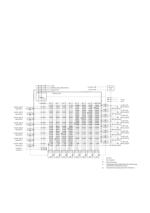
The structure is interposed between the GPIO port and the HSIOM.
Device firmware update (DFU)
The boot ROM supports firmware updates using a serial port. DFU functionality is disabled by default. It needs to be enabled in the OEM policy before use. More details regarding how to enable and use DFU can be found in
AN240106 - Getting started with PSOC™ Control C3 security
.
When enabled, DFU mode selection is initiated during device boot-up depending on the state of P2.2 and P2.3 pins as shown in the table:
P2.3 pin state | P2.2 pin state | DFU mode |
|---|---|---|
High-Z | High-Z | Disable |
High-Z | X | Disable |
X | High-Z | Disable |
Low | Low | Disable |
Low | High | I2C |
High | Low | UART |
High | High | SPI |
X = Don't care
Use pull-up or pull-down resistors of 1 kΩ or less connected to VDDIO_0 or VSS to set these pins to logic high or low. Pins can be left floating for High-Z state. When the device is in DFU mode, the following pins are used for serial communication:
Pin | I2C | UART | SPI |
|---|---|---|---|
P8.0 | CS | ||
P8.1 | SCL | RX | MOSI |
P8.2 | MISO | ||
P8.3 | SDA | TX | CLK |
The following parameters are used for the DFU communication protocols:
I2C: Speed = 400 kHz, Mode = Slave, 7-bit address, address = 0x35
UART: Baud = 115200, Bits = 8, Stop Bits = 1, RTS/CTS = No, Parity = None
SPI: Mode = Slave, Motorola 00 (MSB first, CPHA = 0, CPOL = 0), Speed <= 12 Mbps
Note:
Boot ROM DFU support is available only in 80-pin and 64-pin devices.
Serial wire JTAG debug port/Embedded trace macrocell
Serial wire JTAG debug port (SWJ-DP)
The
PSOC™ Control C3
MCU embeds the ARM® serial wire JTAG debug port (SWJ-DP) which supports 2-wire Serial Wire Debug (SWD) and 4-wire or 5-wire Joint Test Action Group (JTAG) interface. SWD interface is enabled by default after power on and JTAG interface is in disabled state. JTAG can be enabled in 4-wire or 5-wire mode by updating the OEM policy. For more information on updating the OEM policy, refer to the
AN240106 - Getting started with PSOC™ Control C3 security
.
Embedded trace macrocell (ETM)
Arm® embedded trace macrocell is supported by the
PSOC™ Control C3
. It allows reconstruction of program execution using high speed compressed data transmitted on the ETM pins. ETM interface includes a clock (trace.clock) pin and up to four data (trace.data0 to trace.data3) pins.
Pins
GPIO ports and analog inputs are powered by VDDx pins as follows:
P0: VBACKUP
P1, P2, P3, P4, P5, P6, P7: VDDIO_0
P8, P9: VDDIO_1
AN_A, AN_B: AVDD
The number of GPIOs is limited in some packages. The E-LQFP-80 package has the full 50 GPIOs and 16 dedicated analog inputs; the E-LQFP-64/VQNF-64 package has 39 GPIOs and 16 dedicated analog inputs; the E-LQFP-48/VQFN-48 package has 29 GPIOs and 10 dedicated analog inputs. For detailed information on the supported packages, see
gxg1730181873132.html#bcm1697083377157
section.
Pin | Capability | Packages | ||
|---|---|---|---|---|
E-LQFP-80 | E-LQFP-64/VQFN-64 | E-LQFP-48/VQFN-48 | ||
VDDD | - | 9 | 5 | 4 |
VDDA | - | 66 | 54 | 41 |
VDDIO_0_0 | - | 20 | 16 | 12 |
VDDIO_0_1 | - | 40 | 32 | 24 |
VDDIO_0_2 | - | 49 | - | - |
VDDIO_1 | - | 80 | 64 | 48 |
VCCD | - | 10 | 6 | 5 |
VSS | - | GND PAD | GND PAD | GND PAD |
VSS_0 | - | 6 | - | - |
VSS_1 | - | 7 | - | - |
VSS_2 | - | 77 | - | - |
VSS_3 | - | 78 | - | - |
VAREF_EXT | - | 65 | 53 | 40 |
VBACKUP | - | 11 | 7 | 6 |
AN_A0 | AD | 53 | 41 | 31 |
AN_A1 | AD | 54 | 42 | 32 |
AN_A2 | AD | 55 | 43 | 33 |
AN_A3 | AD | 56 | 44 | 34 |
AN_A4 | AD | 57 | 45 | 35 |
AN_A5 | AD | 58 | 46 | 36 |
AN_A6 | AD | 59 | 47 | - |
AN_A7 | AD | 60 | 48 | - |
AN_B0 | AD | 61 | 49 | - |
AN_B1 | AD | 62 | 50 | 37 |
AN_B2 | AD | 63 | 51 | 38 |
AN_B3 | AD | 64 | 52 | 39 |
AN_B4 | AM | 67 | 55 | 42 |
AN_B5 | AM | 68 | 56 | - |
AN_B6 | AM | 69 | 57 | - |
AN_B7 | AM | 70 | 58 | - |
XRES | - | 8 | 4 | 3 |
P0.0 | S | 12 | 8 | 7 |
P0.1 | S | 13 | 9 | - |
P1.0 | S | 14 | 10 | - |
P1.1 | S | 15 | 11 | - |
P1.2 | S | 16 | 12 | 8 |
P1.3 | S | 17 | 13 | 9 |
P2.0 | S | 18 | 14 | 10 |
P2.1 | S | 19 | 15 | 11 |
P2.2 | S | 21 | 17 | 13 |
P2.3 | S | 22 | 18 | 14 |
P3.0 | S | 23 | - | - |
P3.1 | S | 24 | - | - |
P3.2 | S | 25 | - | - |
P3.3 | S | 26 | - | - |
P4.0 | - | 27 | 19 | 15 |
P4.1 | - | 28 | 20 | 16 |
P4.2 | - | 29 | 21 | 17 |
P4.3 | - | 30 | 22 | 18 |
P4.4 | - | 31 | 23 | 19 |
P4.5 | - | 32 | 24 | 20 |
P4.6 | - | 33 | 25 | 21 |
P4.7 | - | 34 | 26 | 22 |
P5.0 | S | 35 | 27 | - |
P5.1 | S | 36 | 28 | - |
P5.2 | S | 37 | 29 | - |
P5.3 | S | 38 | 30 | - |
P6.0 | S | 39 | 31 | 23 |
P6.1 | S | 41 | 33 | 25 |
P6.2 | S | 42 | 34 | 26 |
P6.3 | S | 43 | 35 | 27 |
P7.0 | - | 44 | 36 | 28 |
P7.1 | - | 45 | 37 | 29 |
P7.2 | - | 46 | 38 | 30 |
P7.3 | - | 47 | 39 | - |
P7.4 | - | 48 | 40 | - |
P7.5 | - | 50 | - | - |
P7.6 | - | 51 | - | - |
P7.7 | - | 52 | - | - |
P8.0 | AM, AC | 71 | 59 | 43 |
P8.1 | AM | 72 | 60 | 44 |
P8.2 | AM, AC | 73 | 61 | 45 |
P8.3 | AM | 74 | 62 | 46 |
P8.4 | - | 75 | - | - |
P8.5 | - | 76 | - | - |
P9.0 | S | 79 | 63 | 47 |
P9.1 | S | 1 | 1 | - |
P9.2 | S | 2 | 2 | 1 |
P9.3 | S | 3 | 3 | 2 |
P9.4 | S | 4 | - | - |
P9.5 | S | 5 | - | - |
Abbreviation | Capability |
|---|---|
AD | Dedicated analog pin directly connected to sampler |
AM | Dedicated analog pin/analog capable GPIO pin connected to sampler through MUX |
AC | Analog capable GPIO pin (LPComp input) |
S | Smart IO capable GPIO |
Note:
All GPIO pins are PWM capable. Any TCPWM channel line or line_compl output can be routed to any GPIO pin
Number of LUTs is not impacted by the number of Smart IO capable GPIO pins available in lower pin count packages
Figure 8.
Device pinout for E-LQFP-80 package (top view)
Figure 9.
Device pinout for E-LQFP-64 package (top view)
Figure 10.
Device pinout for VQFN-64 package (top view)
Figure 11.
Device pinout for E-LQFP-48 package (top view)
Figure 12.
Device pinout for VQFN-48 package (top view)
GPIO alternate functions tables
GPIO | Alternate functions and HSIOM routes | |||
|---|---|---|---|---|
P0.0 | wco_out | fixed | smartio0.io0 | fixed |
ext_clk | ACT #8 | peri.tr_io_input[0]:0 | ACT #14 | |
peri.tr_io_output[0]:0 | ACT #15 | |||
P0.1 | wco_in | fixed | smartio0.io1 | fixed |
peri.tr_io_input[1]:0 | ACT #14 | peri.tr_io_output[1]:0 | ACT #15 | |
P1.0 | eco_in | fixed | smartio1.io0 | fixed |
peri.tr_io_output[58]:1 | ACT #1 | peri.tr_io_output[70]:1 | ACT #2 | |
scb1.uart.cts | ACT #4 | scb1.spi.select0 | ACT #6 | |
peri.tr_io_input[2]:0 | ACT #14 | peri.tr_io_output[2]:0 | ACT #15 | |
P1.1 | eco_out | fixed | smartio1.io1 | fixed |
peri.tr_io_output[59]:1 | ACT #1 | peri.tr_io_output[71]:1 | ACT #2 | |
scb1.uart.rts | ACT #4 | scb1.spi.clk | ACT #6 | |
peri.tr_io_input[3]:0 | ACT #14 | peri.tr_io_output[3]:0 | ACT #15 | |
P1.2 | smartio1.io2 | fixed | peri.tr_io_output[60]:1 | ACT #1 |
peri.tr_io_output[72]:1 | ACT #2 | scb1.uart.rx | ACT #4 | |
scb1.spi.mosi | ACT #6 | scb1.i2c.sda | ACT #7 | |
peri.tr_io_input[4]:0 | ACT #14 | peri.tr_io_output[4]:0 | ACT #15 | |
swj.swclk/tclk | DS #5 | |||
P1.3 | smartio1.io3 | fixed | peri.tr_io_output[61]:1 | ACT #1 |
peri.tr_io_output[73]:1 | ACT #2 | scb1.uart.tx | ACT #4 | |
scb1.spi.miso | ACT #6 | scb1.i2c.scl | ACT #7 | |
peri.tr_io_input[5]:0 | ACT #14 | peri.tr_io_output[5]:0 | ACT #15 | |
swj.swdio/tms | DS #5 | |||
P2.0 | hibernate_wakeup | fixed | smartio2.io0 | fixed |
peri.tr_io_output[58]:0 | ACT #1 | tcpwm0.g2.cnt6+ | ACT #2 | |
scb1.uart.cts | ACT #4 | scb1.spi.select0 | ACT #6 | |
peri.tr_io_input[6]:0 | ACT #14 | peri.tr_io_output[6]:0 | ACT #15 | |
swj.tdi | DS #5 | |||
P2.1 | smartio2.io1 | fixed | peri.tr_io_output[59]:0 | ACT #1 |
tcpwm0.g2.cnt6- | ACT #2 | cal_wave | DS #0 | |
scb1.uart.rts | ACT #4 | scb1.spi.clk | ACT #6 | |
scb1.i2c.scl | ACT #7 | peri.tr_io_input[7]:0 | ACT #14 | |
peri.tr_io_output[7]:0 | ACT #15 | swj.tdo | DS #5 | |
P2.2 | smartio2.io2 | fixed | peri.tr_io_output[60]:0 | ACT #1 |
tcpwm0.g2.cnt7+ | ACT #2 | scb1.uart.rx | ACT #4 | |
scb1.spi.mosi | ACT #6 | scb1.i2c.sda | ACT #7 | |
ext_clk | ACT #8 | peri.tr_io_input[8]:0 | ACT #14 | |
peri.tr_io_output[8]:0 | ACT #15 | |||
P2.3 | smartio2.io3 | fixed | peri.tr_io_output[61]:0 | ACT #1 |
tcpwm0.g2.cnt7- | ACT #2 | scb1.uart.tx | ACT #4 | |
scb1.spi.miso | ACT #6 | peri.tr_io_input[9]:0 | ACT #14 | |
peri.tr_io_output[9]:0 | ACT #15 | |||
P3.0 | smartio3.io0 | fixed | peri.tr_io_output[62]:0 | ACT #1 |
scb4.uart.cts | ACT #4 | scb4.spi.mosi | ACT #6 | |
peri.tr_io_input[10]:0 | ACT #14 | peri.tr_io_output[10]:0 | ACT #15 | |
P3.1 | smartio3.io1 | fixed | peri.tr_io_output[63]:0 | ACT #1 |
scb4.uart.rts | ACT #4 | scb4.spi.miso | ACT #6 | |
scb4.i2c.sda | ACT #7 | peri.tr_io_input[11]:0 | ACT #14 | |
peri.tr_io_output[11]:0 | ACT #15 | |||
P3.2 | smartio3.io2 | fixed | peri.tr_io_output[64]:0 | ACT #1 |
scb4.uart.rx | ACT #4 | scb4.spi.clk | ACT #6 | |
scb4.i2c.scl | ACT #7 | peri.tr_io_input[12]:0 | ACT #14 | |
peri.tr_io_output[12]:0 | ACT #15 | |||
P3.3 | smartio3.io3 | fixed | peri.tr_io_output[65]:0 | ACT #1 |
scb4.uart.tx | ACT #4 | scb4.spi.select0 | ACT #6 | |
peri.tr_io_input[13]:0 | ACT #14 | peri.tr_io_output[13]:0 | ACT #15 | |
P4.0 | peri.tr_io_output[50]:0 | ACT #0 | tcpwm0.g1.cnt4+ | ACT #1 |
scb4.uart.cts | ACT #4 | scb4.spi.mosi | ACT #6 | |
peri.tr_io_input[14]:0 | ACT #14 | peri.tr_io_output[14]:0 | ACT #15 | |
P4.1 | peri.tr_io_output[51]:0 | ACT #0 | tcpwm0.g1.cnt4- | ACT #1 |
scb4.uart.rts | ACT #4 | scb4.spi.miso | ACT #6 | |
scb4.i2c.sda | ACT #7 | peri.tr_io_input[15]:0 | ACT #14 | |
peri.tr_io_output[15]:0 | ACT #15 | |||
P4.2 | peri.tr_io_output[52]:0 | ACT #0 | tcpwm0.g1.cnt5+ | ACT #1 |
scb4.uart.rx | ACT #4 | scb4.spi.clk | ACT #6 | |
scb4.i2c.scl | ACT #7 | peri.tr_io_input[16]:0 | ACT #14 | |
peri.tr_io_output[16]:0 | ACT #15 | |||
P4.3 | peri.tr_io_output[53]:0 | ACT #0 | tcpwm0.g1.cnt5- | ACT #1 |
scb4.uart.tx | ACT #4 | scb4.spi.select0 | ACT #6 | |
peri.tr_io_input[17]:0 | ACT #14 | peri.tr_io_output[17]:0 | ACT #15 | |
P4.4 | peri.tr_io_output[54]:0 | ACT #0 | tcpwm0.g1.cnt6+ | ACT #1 |
peri.tr_io_input[18]:0 | ACT #14 | peri.tr_io_output[18]:0 | ACT #15 | |
P4.5 | peri.tr_io_output[55]:0 | ACT #0 | tcpwm0.g1.cnt6- | ACT #1 |
peri.tr_io_input[19]:0 | ACT #14 | peri.tr_io_output[19]:0 | ACT #15 | |
P4.6 | peri.tr_io_output[56]:0 | ACT #0 | tcpwm0.g1.cnt7+ | ACT #1 |
peri.tr_io_input[20]:0 | ACT #14 | peri.tr_io_output[20]:0 | ACT #15 | |
P4.7 | peri.tr_io_output[57]:0 | ACT #0 | tcpwm0.g1.cnt7- | ACT #1 |
peri.tr_io_input[21]:0 | ACT #14 | peri.tr_io_output[21]:0 | ACT #15 | |
P5.0 | smartio5.io0 | fixed | peri.tr_io_output[62]:1 | ACT #1 |
scb3.uart.cts | ACT #4 | scb3.spi.mosi | ACT #6 | |
scb3.i2c.sda | ACT #7 | peri.tr_io_input[22]:0 | ACT #14 | |
peri.tr_io_output[22]:0 | ACT #15 | |||
P5.1 | smartio5.io1 | fixed | peri.tr_io_output[63]:1 | ACT #1 |
scb3.uart.rts | ACT #4 | scb3.spi.miso | ACT #6 | |
scb3.i2c.scl | ACT #7 | peri.tr_io_input[23]:0 | ACT #14 | |
peri.tr_io_output[23]:0 | ACT #15 | |||
P5.2 | smartio5.io2 | fixed | peri.tr_io_output[64]:1 | ACT #1 |
can1.rx | ACT #3 | scb3.uart.rx | ACT #4 | |
scb3.spi.clk | ACT #6 | peri.tr_io_input[24]:0 | ACT #14 | |
peri.tr_io_output[24]:0 | ACT #15 | |||
P5.3 | smartio5.io3 | fixed | peri.tr_io_output[65]:1 | ACT #1 |
can1.tx | ACT #3 | scb3.uart.tx | ACT #4 | |
scb3.spi.select0 | ACT #6 | peri.tr_io_input[25]:0 | ACT #14 | |
peri.tr_io_output[25]:0 | ACT #15 | |||
P6.0 | smartio6.io0 | fixed | tcpwm0.g1.cnt4+ | ACT #1 |
peri.tr_io_output[66]:0 | ACT #2 | scb3.uart.cts | ACT #4 | |
scb3.spi.mosi | ACT #6 | scb3.i2c.sda | ACT #7 | |
peri.tr_io_input[26]:0 | ACT #14 | peri.tr_io_output[26]:0 | ACT #15 | |
P6.1 | smartio6.io1 | fixed | tcpwm0.g1.cnt4- | ACT #1 |
peri.tr_io_output[67]:0 | ACT #2 | scb3.uart.rts | ACT #4 | |
scb3.spi.miso | ACT #6 | scb3.i2c.scl | ACT #7 | |
peri.tr_io_input[27]:0 | ACT #14 | peri.tr_io_output[27]:0 | ACT #15 | |
P6.2 | smartio6.io2 | fixed | tcpwm0.g1.cnt5+ | ACT #1 |
peri.tr_io_output[68]:0 | ACT #2 | can1.rx | ACT #3 | |
scb3.uart.rx | ACT #4 | scb3.spi.clk | ACT #6 | |
peri.tr_io_input[28]:0 | ACT #14 | peri.tr_io_output[28]:0 | ACT #15 | |
P6.3 | smartio6.io3 | fixed | tcpwm0.g1.cnt5- | ACT #1 |
peri.tr_io_output[69]:0 | ACT #2 | can1.tx | ACT #3 | |
scb3.uart.tx | ACT #4 | scb3.spi.select0 | ACT #6 | |
cpuss.fault[0]:1 | ACT #9 | peri.tr_io_input[29]:0 | ACT #14 | |
peri.tr_io_output[29]:0 | ACT #15 | |||
P7.0 | peri.tr_io_output[50]:1 | ACT #0 | tcpwm0.g1.cnt6+ | ACT #1 |
peri.tr_io_output[70]:0 | ACT #2 | scb2.uart.cts | ACT #4 | |
scb2.spi.clk | ACT #5 | scb2.i2c.scl | ACT #7 | |
trace.data0 | ACT #9 | hppass.gpio_out0 | ACT #12 | |
peri.tr_io_input[30]:0 | ACT #14 | peri.tr_io_output[30]:0 | ACT #15 | |
P7.1 | peri.tr_io_output[51]:1 | ACT #0 | tcpwm0.g1.cnt6- | ACT #1 |
peri.tr_io_output[71]:0 | ACT #2 | scb2.uart.tx | ACT #4 | |
scb2.spi.mosi | ACT #5 | scb2.i2c.sda | ACT #7 | |
trace.data1 | ACT #9 | hppass.gpio_out1 | ACT #12 | |
peri.tr_io_input[31]:0 | ACT #14 | peri.tr_io_output[31]:0 | ACT #15 | |
P7.2 | peri.tr_io_output[52]:1 | ACT #0 | tcpwm0.g1.cnt7+ | ACT #1 |
peri.tr_io_output[72]:0 | ACT #2 | scb2.uart.rx | ACT #4 | |
scb2.spi.miso | ACT #5 | trace.data2 | ACT #9 | |
hppass.gpio_out2 | ACT #12 | peri.tr_io_input[32]:0 | ACT #14 | |
peri.tr_io_output[32]:0 | ACT #15 | |||
P7.3 | peri.tr_io_output[53]:1 | ACT #0 | tcpwm0.g1.cnt7- | ACT #1 |
peri.tr_io_output[73]:0 | ACT #2 | scb2.uart.rts | ACT #4 | |
scb2.spi.select0 | ACT #5 | trace.data3 | ACT #9 | |
hppass.gpio_out3 | ACT #12 | peri.tr_io_input[33]:0 | ACT #14 | |
peri.tr_io_output[33]:0 | ACT #15 | |||
P7.4 | peri.tr_io_output[54]:1 | ACT #0 | scb2.spi.select1 | ACT #5 |
trace.clock | ACT #9 | hppass.gpio_out4 | ACT #12 | |
peri.tr_io_input[34]:0 | ACT #14 | peri.tr_io_output[34]:0 | ACT #15 | |
P7.5 | peri.tr_io_output[55]:1 | ACT #0 | scb2.spi.select2 | ACT #5 |
peri.tr_io_input[35]:0 | ACT #14 | peri.tr_io_output[35]:0 | ACT #15 | |
P7.6 | peri.tr_io_output[56]:1 | ACT #0 | peri.tr_io_input[36]:0 | ACT #14 |
peri.tr_io_output[36]:0 | ACT #15 | |||
P7.7 | peri.tr_io_output[57]:1 | ACT #0 | peri.tr_io_input[37]:0 | ACT #14 |
peri.tr_io_output[37]:0 | ACT #15 | |||
P8.0 | lpcomp0.in+ | fixed | hppass.gpio_00_aio | fixed |
peri.tr_io_output[62]:2 | ACT #1 | tcpwm0.g2.cnt4+ | ACT #2 | |
scb5.uart.cts | ACT #4 | scb5.spi.select0 | ACT #5 | |
trace.data0 | ACT #9 | hppass.gpio_out0 | ACT #12 | |
peri.tr_io_input[38]:0 | ACT #14 | peri.tr_io_output[38]:0 | ACT #15 | |
swj.trstn | DS #5 | |||
P8.1 | lpcomp0.in- | fixed | peri.tr_io_output[63]:2 | ACT #1 |
tcpwm0.g2.cnt4- | ACT #2 | scb5.uart.rx | ACT #4 | |
scb5.spi.mosi | ACT #5 | scb5.i2c.scl | ACT #7 | |
trace.data1 | ACT #9 | hppass.gpio_out1 | ACT #12 | |
peri.tr_io_input[39]:0 | ACT #14 | peri.tr_io_output[39]:0 | ACT #15 | |
P8.2 | lpcomp1.in+ | fixed | hppass.gpio_01_aio | fixed |
peri.tr_io_output[64]:2 | ACT #1 | tcpwm0.g2.cnt5+ | ACT #2 | |
can0.rx | ACT #3 | scb5.uart.rts | ACT #4 | |
scb5.spi.miso | ACT #5 | trace.data2 | ACT #9 | |
hppass.gpio_out2 | ACT #12 | peri.tr_io_input[40]:0 | ACT #14 | |
peri.tr_io_output[40]:0 | ACT #15 | |||
P8.3 | lpcomp1.in- | fixed | peri.tr_io_output[65]:2 | ACT #1 |
tcpwm0.g2.cnt5- | ACT #2 | can0.tx | ACT #3 | |
scb5.uart.tx | ACT #4 | scb5.spi.clk | ACT #5 | |
scb5.i2c.sda | ACT #7 | trace.data3 | ACT #9 | |
hppass.gpio_out3 | ACT #12 | peri.tr_io_input[41]:0 | ACT #14 | |
peri.tr_io_output[41]:0 | ACT #15 | |||
P8.4 | scb5.spi.select1 | ACT #5 | peri.tr_io_input[42]:0 | ACT #14 |
peri.tr_io_output[42]:0 | ACT #15 | |||
P8.5 | scb5.spi.select2 | ACT #5 | peri.tr_io_input[43]:0 | ACT #14 |
peri.tr_io_output[43]:0 | ACT #15 | |||
P9.0 | hibernate_wakeup | fixed | smartio9.io0 | fixed |
tcpwm0.g2.cnt6+ | ACT #2 | scb0.spi.clk | DS #1 | |
scb0.uart.cts | DS #2 | scb0.i2c.scl | DS #3 | |
peri.tr_io_input[44]:0 | ACT #14 | peri.tr_io_output[44]:0 | ACT #15 | |
P9.1 | smartio9.io1 | fixed | tcpwm0.g2.cnt6- | ACT #2 |
scb0.spi.select0 | DS #1 | scb0.uart.rts | DS #2 | |
peri.tr_io_input[45]:0 | ACT #14 | peri.tr_io_output[45]:0 | ACT #15 | |
P9.2 | smartio9.io2 | fixed | tcpwm0.g2.cnt7+ | ACT #2 |
can0.rx | ACT #3 | scb0.spi.mosi | DS #1 | |
scb0.uart.rx | DS #2 | scb0.i2c.sda | DS #3 | |
trace.clock | ACT #9 | hppass.gpio_out4 | ACT #12 | |
peri.tr_io_input[46]:0 | ACT #14 | peri.tr_io_output[46]:0 | ACT #15 | |
P9.3 | smartio9.io3 | fixed | tcpwm0.g2.cnt7- | ACT #2 |
can0.tx | ACT #3 | scb0.spi.miso | DS #1 | |
scb0.uart.tx | DS #2 | cpuss.clk_fm_pump | ACT #8 | |
cpuss.fault[0]:0 | ACT #9 | peri.tr_io_input[47]:0 | ACT #14 | |
peri.tr_io_output[47]:0 | ACT #15 | |||
P9.4 | smartio9.io4 | fixed | scb0.spi.select1 | DS #1 |
peri.tr_io_input[48]:0 | ACT #14 | peri.tr_io_output[48]:0 | ACT #15 | |
P9.5 | vext_ref_reg | fixed | smartio9.io5 | fixed |
scb0.spi.select2 | DS #1 | peri.tr_io_input[49]:0 | ACT #14 | |
peri.tr_io_output[49]:0 | ACT #15 | |||
Function | GPIOs | Function | GPIOs | Function | GPIOs |
|---|---|---|---|---|---|
cal_wave | P2.1 | can0.rx | P8.2, P9.2 | can0.tx | P8.3, P9.3 |
can1.rx | P5.2, P6.2 | can1.tx | P5.3, P6.3 | cpuss.clk_fm_pump | P9.3 |
cpuss.fault[0]:0 | P9.3 | cpuss.fault[0]:1 | P6.3 | eco_in | P1.0 |
eco_out | P1.1 | ext_clk | P0.0, P2.2 | hibernate_wakeup | P2.0, P9.0 |
hppass.gpio_00_aio | P8.0 | hppass.gpio_01_aio | P8.2 | hppass.gpio_out0 | P7.0, P8.0 |
hppass.gpio_out1 | P7.1, P8.1 | hppass.gpio_out2 | P7.2, P8.2 | hppass.gpio_out3 | P7.3, P8.3 |
hppass.gpio_out4 | P7.4, P9.2 | lpcomp0.in+ | P8.0 | lpcomp0.in- | P8.1 |
lpcomp1.in+ | P8.2 | lpcomp1.in- | P8.3 | peri.tr_io_input[0]:0 | P0.0 |
peri.tr_io_input[10]:0 | P3.0 | peri.tr_io_input[11]:0 | P3.1 | peri.tr_io_input[12]:0 | P3.2 |
peri.tr_io_input[13]:0 | P3.3 | peri.tr_io_input[14]:0 | P4.0 | peri.tr_io_input[15]:0 | P4.1 |
peri.tr_io_input[16]:0 | P4.2 | peri.tr_io_input[17]:0 | P4.3 | peri.tr_io_input[18]:0 | P4.4 |
peri.tr_io_input[19]:0 | P4.5 | peri.tr_io_input[1]:0 | P0.1 | peri.tr_io_input[20]:0 | P4.6 |
peri.tr_io_input[21]:0 | P4.7 | peri.tr_io_input[22]:0 | P5.0 | peri.tr_io_input[23]:0 | P5.1 |
peri.tr_io_input[24]:0 | P5.2 | peri.tr_io_input[25]:0 | P5.3 | peri.tr_io_input[26]:0 | P6.0 |
peri.tr_io_input[27]:0 | P6.1 | peri.tr_io_input[28]:0 | P6.2 | peri.tr_io_input[29]:0 | P6.3 |
peri.tr_io_input[2]:0 | P1.0 | peri.tr_io_input[30]:0 | P7.0 | peri.tr_io_input[31]:0 | P7.1 |
peri.tr_io_input[32]:0 | P7.2 | peri.tr_io_input[33]:0 | P7.3 | peri.tr_io_input[34]:0 | P7.4 |
peri.tr_io_input[35]:0 | P7.5 | peri.tr_io_input[36]:0 | P7.6 | peri.tr_io_input[37]:0 | P7.7 |
peri.tr_io_input[38]:0 | P8.0 | peri.tr_io_input[39]:0 | P8.1 | peri.tr_io_input[3]:0 | P1.1 |
peri.tr_io_input[40]:0 | P8.2 | peri.tr_io_input[41]:0 | P8.3 | peri.tr_io_input[42]:0 | P8.4 |
peri.tr_io_input[43]:0 | P8.5 | peri.tr_io_input[44]:0 | P9.0 | peri.tr_io_input[45]:0 | P9.1 |
peri.tr_io_input[46]:0 | P9.2 | peri.tr_io_input[47]:0 | P9.3 | peri.tr_io_input[48]:0 | P9.4 |
peri.tr_io_input[49]:0 | P9.5 | peri.tr_io_input[4]:0 | P1.2 | peri.tr_io_input[5]:0 | P1.3 |
peri.tr_io_input[6]:0 | P2.0 | peri.tr_io_input[7]:0 | P2.1 | peri.tr_io_input[8]:0 | P2.2 |
peri.tr_io_input[9]:0 | P2.3 | peri.tr_io_output[0]:0 | P0.0 | peri.tr_io_output[10]:0 | P3.0 |
peri.tr_io_output[11]:0 | P3.1 | peri.tr_io_output[12]:0 | P3.2 | peri.tr_io_output[13]:0 | P3.3 |
peri.tr_io_output[14]:0 | P4.0 | peri.tr_io_output[15]:0 | P4.1 | peri.tr_io_output[16]:0 | P4.2 |
peri.tr_io_output[17]:0 | P4.3 | peri.tr_io_output[18]:0 | P4.4 | peri.tr_io_output[19]:0 | P4.5 |
peri.tr_io_output[1]:0 | P0.1 | peri.tr_io_output[20]:0 | P4.6 | peri.tr_io_output[21]:0 | P4.7 |
peri.tr_io_output[22]:0 | P5.0 | peri.tr_io_output[23]:0 | P5.1 | peri.tr_io_output[24]:0 | P5.2 |
peri.tr_io_output[25]:0 | P5.3 | peri.tr_io_output[26]:0 | P6.0 | peri.tr_io_output[27]:0 | P6.1 |
peri.tr_io_output[28]:0 | P6.2 | peri.tr_io_output[29]:0 | P6.3 | peri.tr_io_output[2]:0 | P1.0 |
peri.tr_io_output[30]:0 | P7.0 | peri.tr_io_output[31]:0 | P7.1 | peri.tr_io_output[32]:0 | P7.2 |
peri.tr_io_output[33]:0 | P7.3 | peri.tr_io_output[34]:0 | P7.4 | peri.tr_io_output[35]:0 | P7.5 |
peri.tr_io_output[36]:0 | P7.6 | peri.tr_io_output[37]:0 | P7.7 | peri.tr_io_output[38]:0 | P8.0 |
peri.tr_io_output[39]:0 | P8.1 | peri.tr_io_output[3]:0 | P1.1 | peri.tr_io_output[40]:0 | P8.2 |
peri.tr_io_output[41]:0 | P8.3 | peri.tr_io_output[42]:0 | P8.4 | peri.tr_io_output[43]:0 | P8.5 |
peri.tr_io_output[44]:0 | P9.0 | peri.tr_io_output[45]:0 | P9.1 | peri.tr_io_output[46]:0 | P9.2 |
peri.tr_io_output[47]:0 | P9.3 | peri.tr_io_output[48]:0 | P9.4 | peri.tr_io_output[49]:0 | P9.5 |
peri.tr_io_output[4]:0 | P1.2 | peri.tr_io_output[50]:0 | P4.0 | peri.tr_io_output[50]:1 | P7.0 |
peri.tr_io_output[51]:0 | P4.1 | peri.tr_io_output[51]:1 | P7.1 | peri.tr_io_output[52]:0 | P4.2 |
peri.tr_io_output[52]:1 | P7.2 | peri.tr_io_output[53]:0 | P4.3 | peri.tr_io_output[53]:1 | P7.3 |
peri.tr_io_output[54]:0 | P4.4 | peri.tr_io_output[54]:1 | P7.4 | peri.tr_io_output[55]:0 | P4.5 |
peri.tr_io_output[55]:1 | P7.5 | peri.tr_io_output[56]:0 | P4.6 | peri.tr_io_output[56]:1 | P7.6 |
peri.tr_io_output[57]:0 | P4.7 | peri.tr_io_output[57]:1 | P7.7 | peri.tr_io_output[58]:0 | P2.0 |
peri.tr_io_output[58]:1 | P1.0 | peri.tr_io_output[59]:0 | P2.1 | peri.tr_io_output[59]:1 | P1.1 |
peri.tr_io_output[5]:0 | P1.3 | peri.tr_io_output[60]:0 | P2.2 | peri.tr_io_output[60]:1 | P1.2 |
peri.tr_io_output[61]:0 | P2.3 | peri.tr_io_output[61]:1 | P1.3 | peri.tr_io_output[62]:0 | P3.0 |
peri.tr_io_output[62]:1 | P5.0 | peri.tr_io_output[62]:2 | P8.0 | peri.tr_io_output[63]:0 | P3.1 |
peri.tr_io_output[63]:1 | P5.1 | peri.tr_io_output[63]:2 | P8.1 | peri.tr_io_output[64]:0 | P3.2 |
peri.tr_io_output[64]:1 | P5.2 | peri.tr_io_output[64]:2 | P8.2 | peri.tr_io_output[65]:0 | P3.3 |
peri.tr_io_output[65]:1 | P5.3 | peri.tr_io_output[65]:2 | P8.3 | peri.tr_io_output[66]:0 | P6.0 |
peri.tr_io_output[67]:0 | P6.1 | peri.tr_io_output[68]:0 | P6.2 | peri.tr_io_output[69]:0 | P6.3 |
peri.tr_io_output[6]:0 | P2.0 | peri.tr_io_output[70]:0 | P7.0 | peri.tr_io_output[70]:1 | P1.0 |
peri.tr_io_output[71]:0 | P7.1 | peri.tr_io_output[71]:1 | P1.1 | peri.tr_io_output[72]:0 | P7.2 |
peri.tr_io_output[72]:1 | P1.2 | peri.tr_io_output[73]:0 | P7.3 | peri.tr_io_output[73]:1 | P1.3 |
peri.tr_io_output[7]:0 | P2.1 | peri.tr_io_output[8]:0 | P2.2 | peri.tr_io_output[9]:0 | P2.3 |
scb0.i2c.scl | P9.0 | scb0.i2c.sda | P9.2 | scb0.spi.clk | P9.0 |
scb0.spi.miso | P9.3 | scb0.spi.mosi | P9.2 | scb0.spi.select0 | P9.1 |
scb0.spi.select1 | P9.4 | scb0.spi.select2 | P9.5 | scb0.uart.cts | P9.0 |
scb0.uart.rts | P9.1 | scb0.uart.rx | P9.2 | scb0.uart.tx | P9.3 |
scb1.i2c.scl | P1.3, P2.1 | scb1.i2c.sda | P1.2, P2.2 | scb1.spi.clk | P1.1, P2.1 |
scb1.spi.miso | P1.3, P2.3 | scb1.spi.mosi | P1.2, P2.2 | scb1.spi.select0 | P1.0, P2.0 |
scb1.uart.cts | P1.0, P2.0 | scb1.uart.rts | P1.1, P2.1 | scb1.uart.rx | P1.2, P2.2 |
scb1.uart.tx | P1.3, P2.3 | scb2.i2c.scl | P7.0 | scb2.i2c.sda | P7.1 |
scb2.spi.clk | P7.0 | scb2.spi.miso | P7.2 | scb2.spi.mosi | P7.1 |
scb2.spi.select0 | P7.3 | scb2.spi.select1 | P7.4 | scb2.spi.select2 | P7.5 |
scb2.uart.cts | P7.0 | scb2.uart.rts | P7.3 | scb2.uart.rx | P7.2 |
scb2.uart.tx | P7.1 | scb3.i2c.scl | P5.1, P6.1 | scb3.i2c.sda | P5.0, P6.0 |
scb3.spi.clk | P5.2, P6.2 | scb3.spi.miso | P5.1, P6.1 | scb3.spi.mosi | P5.0, P6.0 |
scb3.spi.select0 | P5.3, P6.3 | scb3.uart.cts | P5.0, P6.0 | scb3.uart.rts | P5.1, P6.1 |
scb3.uart.rx | P5.2, P6.2 | scb3.uart.tx | P5.3, P6.3 | scb4.i2c.scl | P3.2, P4.2 |
scb4.i2c.sda | P3.1, P4.1 | scb4.spi.clk | P3.2, P4.2 | scb4.spi.miso | P3.1, P4.1 |
scb4.spi.mosi | P3.0, P4.0 | scb4.spi.select0 | P3.3, P4.3 | scb4.uart.cts | P3.0, P4.0 |
scb4.uart.rts | P3.1, P4.1 | scb4.uart.rx | P3.2, P4.2 | scb4.uart.tx | P3.3, P4.3 |
scb5.i2c.scl | P8.1 | scb5.i2c.sda | P8.3 | scb5.spi.clk | P8.3 |
scb5.spi.miso | P8.2 | scb5.spi.mosi | P8.1 | scb5.spi.select0 | P8.0 |
scb5.spi.select1 | P8.4 | scb5.spi.select2 | P8.5 | scb5.uart.cts | P8.0 |
scb5.uart.rts | P8.2 | scb5.uart.rx | P8.1 | scb5.uart.tx | P8.3 |
smartio0.io0 | P0.0 | smartio0.io1 | P0.1 | smartio1.io0 | P1.0 |
smartio1.io1 | P1.1 | smartio1.io2 | P1.2 | smartio1.io3 | P1.3 |
smartio2.io0 | P2.0 | smartio2.io1 | P2.1 | smartio2.io2 | P2.2 |
smartio2.io3 | P2.3 | smartio3.io0 | P3.0 | smartio3.io1 | P3.1 |
smartio3.io2 | P3.2 | smartio3.io3 | P3.3 | smartio5.io0 | P5.0 |
smartio5.io1 | P5.1 | smartio5.io2 | P5.2 | smartio5.io3 | P5.3 |
smartio6.io0 | P6.0 | smartio6.io1 | P6.1 | smartio6.io2 | P6.2 |
smartio6.io3 | P6.3 | smartio9.io0 | P9.0 | smartio9.io1 | P9.1 |
smartio9.io2 | P9.2 | smartio9.io3 | P9.3 | smartio9.io4 | P9.4 |
smartio9.io5 | P9.5 | swj.swclk/tclk | P1.2 | swj.swdio/tms | P1.3 |
swj.tdi | P2.0 | swj.tdo | P2.1 | swj.trstn | P8.0 |
tcpwm0.g1.cnt4+ | P4.0, P6.0 | tcpwm0.g1.cnt4- | P4.1, P6.1 | tcpwm0.g1.cnt5+ | P4.2, P6.2 |
tcpwm0.g1.cnt5- | P4.3, P6.3 | tcpwm0.g1.cnt6+ | P4.4, P7.0 | tcpwm0.g1.cnt6- | P4.5, P7.1 |
tcpwm0.g1.cnt7+ | P4.6, P7.2 | tcpwm0.g1.cnt7- | P4.7, P7.3 | tcpwm0.g2.cnt4+ | P8.0 |
tcpwm0.g2.cnt4- | P8.1 | tcpwm0.g2.cnt5+ | P8.2 | tcpwm0.g2.cnt5- | P8.3 |
tcpwm0.g2.cnt6+ | P2.0, P9.0 | tcpwm0.g2.cnt6- | P2.1, P9.1 | tcpwm0.g2.cnt7+ | P2.2, P9.2 |
tcpwm0.g2.cnt7- | P2.3, P9.3 | trace.clock | P7.4, P9.2 | trace.data0 | P7.0, P8.0 |
trace.data1 | P7.1, P8.1 | trace.data2 | P7.2, P8.2 | trace.data3 | P7.3, P8.3 |
vext_ref_reg | P9.5 | wco_in | P0.1 | wco_out | P0.0 |
The peri.tr_io_input[n] and peri.tr_io_output[n] provide one more level of trigger and signal routing option between the peripherals and the GPIO pins using the high-speed I/O matrix (HSIOM). The peri.tr_io_input[n] allows a GPIO pin to be used as peripheral trigger input source (external trigger). Similarly, the peri.tr_io_output[n] can be used to route peripheral triggers and some signals like TCPWM line_out and line_compl_out to a GPIO pin. For more information refer to the Trigger MUX connection tables in section 10.3 of the PSOC™ Control C3 architecture reference manual.
Electrical specifications
Absolute maximum ratings
Spec ID | Parameter | Symbol | Values | Unit | Note or test condition | ||
|---|---|---|---|---|---|---|---|
Min. | Typ. | Max. | |||||
SID1 | Analog or Digital Supply relative to Vss (Vssd=Vssa) | VDD_ABS | -0.5 | - | 4 | V | Absolute Maximum |
SID2 | Direct digital core voltage input relative to Vssd | VCCD_ABS | -0.5 | - | 1.2 | V | Absolute Maximum |
SID3 | GPIO voltage ; VDDD or VDDA | VGPIO_ABS | -0.5 | - | VDD+0.5 | V | Absolute Maximum |
SID4 | Current per GPIO | IGPIO_ABS | -25 | - | 25 | mA | Absolute Maximum |
SID5 | GPIO injection current per pin | IGPIO_injection | -0.5 | - | 0.5 | mA | Absolute Maximum |
SID3A | Electrostatic discharge Human Body Model | ESD_HBM | 2000 | - | - | V | Absolute Maximum |
SID4A | Electrostatic discharge Charged Device Model | ESD_CDM | 500 | - | - | V | Absolute Maximum |
SID5A | Pin current for latchup free operation | LU | -100 | - | 100 | mA | Absolute Maximum |
SIDWA8 | Maximum undershoot voltage for I/O | Vundershoot | - | - | -0.5 | V | Duration not to exceed 25% of the duty cycle |
SIDWA9 | Maximum overshoot voltage for I/O | Vovershoot | - | - | VDDIO + 0.5 | V | Duration not to exceed 25% of the duty cycle |
SIDWA10 | Maximum junction temperature | Tj | - | - | 125 | °C | |
Device level specifications
Power supplies
Spec ID | Parameter | Symbol | Values | Unit | Note or test condition | ||
|---|---|---|---|---|---|---|---|
Min. | Typ. | Max. | |||||
| DC Specifications | |||||||
SID6 | Internal Regulator | VDDD | 1.71 | - | 3.6 | V | |
SID7B | GPIO Supply for Ports 1, 2, 3, 4, 5, 6, 7 | VDDIO_0 | 1.71 | - | 3.6 | V | |
SID7EP | E-Fuse Programming time | EFUSETIME | - | - | 5.5 | μs | Switch on time of 0.5us included |
SID7C | GPIO Supply for Ports 8 and 9 | VDDIO_1 | 1.71 | - | 3.6 | V | |
SID7A | Analog power supply for ADC and Comparator | VDDA | 1.71 | - | 3.6 | V | |
SID6B | Backup Power; normally shorted to VDDD (supply PORT 0) | VBACKUP | 1.71 | - | 3.6 | V | Min. is 1.4 V in Backup mode |
SID8 | Output voltage (for core logic bypass) | VCCD (OD) | - | 1.2 | - | V | Over drive mode |
SID8A | Output voltage (for core logic bypass) | VCCD (LP) | - | 1.1 | - | V | High-speed mode |
SID8B | Output voltage (for core logic bypass) | VCCD (MF) | - | 1 | - | ULP mode. Valid for -20 to 125°C. | |
SID8C | Output voltage (for core logic bypass) | VCCD (ULP) | - | 0.9 | - | ULP mode. Valid for -20 to 125°C. | |
SID10 | External Regulator voltage (VCCD) bypass | CEFC | 3.76 | 4.7 | 5.6 | µF | X5R ceramic or better. Value for 0.8 to 1.1 V. |
SID11 | Power supply decoupling capacitor | CEXC | - | 10 | - | µF | X5R ceramic or better |
Deep Sleep Mode | |||||||
SIDDS1 | With internal LDO enabled and no SRAM retention | IDD33 | - | 6 | 8 | µA | Max value is at 85°C (not including analog leakage on VDDA and VAREF_EXT) |
SIDDS1_A | With internal LDO enabled and 64K SRAM retention | IDD33A | - | 7 | 11 | µA | Max value is at 85°C (not including analog leakage on VDDA and VAREF_EXT) |
| Hibernate Mode | |||||||
SIDHIB1 | VDDD = 1.8 V | IDD34 | - | 300 | - | nA | No clocks running (not including analog leakage on VDDA and VAREF_EXT) |
SIDHIB2 | VDDD = 3.3 V | IDD34A | - | 500 | - | nA | No clocks running (not including analog leakage on VDDA and VAREF_EXT) |
SIDHIB3 | VDDD = 1.8 V | IDD35 | - | 800 | - | nA | WCO is running, lpcomp active (not including analog leakage on VDDA and VAREF_EXT) |
SIDHIB4 | VDDD = 3.3 V | IDD35A | - | 1000 | - | nA | WCO is running, lpcomp active (not including analog leakage on VDDA and VAREF_EXT) |
SIDHIB5 | Leakage on analog supply and analog reference in hibernate mode | IDDA | - | 100 | - | nA | Typical silicon and typical temperature |
CPU currents and transition times
Spec ID | Parameter | Symbol | Values | Unit | Note or test condition | ||
|---|---|---|---|---|---|---|---|
Min. | Typ. | Max. | |||||
| Cortex® M33. Active Mode | |||||||
SIDC2 | Execute from Cache;CM33 Active 180 MHz. PLL. Dhrystone. OD mode | IDD4 | - | 25 | 45 | mA | VDDD=3.3 V, Max at 125°C |
SIDC2A | Execute from Cache;CM33 Active 180 MHz. PLL. Dhrystone. OD mode | IDD4A | - | 25 | 45 | mA | VDDD=1.8 V, Max at 125°C |
SIDC3 | Execute from Cache;CM33 Active 150 MHz. PLL. Dhrystone. LP Mode | IDD5 | - | 18 | 35 | mA | VDDD=3.3 V, Max at 125°C |
SIDC3A | Execute from Cache;CM33 Active 150 MHz. PLL. Dhrystone. LP Mode | IDD5A | - | 18 | 35 | mA | VDDD=1.8 V, Max at 125°C |
SIDC4 | Execute from Cache;CM33 Active 70 MHz. PLL. Dhrystone. MF Mode | IDD6 | - | 12 | 27 | mA | VDDD=3.3 V, Max at 125°C |
SIDC4A | Execute from Cache;CM33 Active 70 MHz. PLL. Dhrystone. MF Mode | IDD6A | - | 12 | 27 | mA | VDDD=1.8 V, Max at 125°C |
SIDC5 | Execute from Cache;CM33 Active 50 MHz. PLL. Dhrystone. ULP Mode | IDD7 | - | 7 | 18 | mA | VDDD=3.3 V, Max at 125°C |
SIDC5A | Execute from Cache;CM33 Active 50 MHz. PLL. Dhrystone. ULP Mode | IDD7A | - | 7 | 18 | mA | VDDD=1.8 V, Max at 125°C |
| Cortex® M33 Sleep Mode | |||||||
SIDS1 | CM33 Sleep 180 MHz. PLL. OD Mode | IDD11 | - | 10 | 15 | mA | VDDD=3.3 V, Max at 105°C |
SIDS1A | CM33 Sleep 180 MHz. PLL. OD Mode | IDD11A | - | 10 | 15 | mA | VDDD=1.8 V, Max at 105°C |
SIDS2 | CM33 Sleep 150 MHz. PLL. LP Mode | IDD12 | - | 7 | 11 | mA | VDDD=3.3 V, Max at 105°C |
SIDS2A | CM33 Sleep 150 MHz. PLL. LP Mode | IDD12A | - | 7.0 | 11 | mA | VDDD=1.8 V, Max at 105°C |
SIDS3 | CM33 Sleep 70 MHz. PLL. MF Mode | IDD13 | - | 4.5 | 10 | mA | VDDD=3.3 V, Max at 105°C |
SIDS3A | CM33 Sleep 70 MHz. PLL. MF Mode | IDD13A | - | 4.5 | 10 | mA | VDDD=1.8 V, Max at 105°C |
SIDS4 | CM33 Sleep 50 MHz. PLL. ULP Mode | IDD14 | - | 4 | 9 | mA | VDDD=3.3 V, Max at 105°C |
SIDS4A | CM33 Sleep 50 MHz. PLL. ULP Mode | IDD14A | - | 4 | 9 | mA | VDDD=1.8 V, Max at 105°C |
| Boot Time | |||||||
SIDBT1 | Boot time after reset | BTIME | - | - | 3000000 | cycles | Refer to CPU clock cycles |
| Power Mode Transition Times | |||||||
SID13A | Deep Sleep to Active transition time. | TDS_ACT | - | - | 45 | µs | DS to Active with 1.1 V operation |
SID13B | Deep Sleep to Active LP transition time | TDS_ACTLP | - | - | 26 | µs | DS to Active LP with 1.0 V operation |
SID13C | Deep Sleep-RAM to Active transition time | TDSR_ACT | - | - | 800 | µs | DS to Active with 1.1 V operation |
SID13D | Deep Sleep-RAM to Active LP transition time | TDSR_ACTULP | - | - | 800 | µs | DS-RAM to Active LP with 1.0 V operation |
SID14 | Hibernate to Active transition time | THIB_ACT | - | 2000 | - | µS | Including PLL lock time |
XRES
Spec ID | Parameter | Symbol | Values | Unit | Note or test condition | ||
|---|---|---|---|---|---|---|---|
Min. | Typ. | Max. | |||||
| XRES AC Specifications | |||||||
SID15 | POR or XRES release to Active transition time | TXRES_ACT | - | 2 | - | mS | With BOOT_OD_CLOCK=180MHz, LISTEN_WINDOW=9 and BOOT_SIMPLE_APP configuration |
SID16 | XRES Pulse width | TXRES_PW | 5 | - | - | µS | |
| XRES DC Specifications | |||||||
SID17 | IDD when XRES asserted | TXRES_IDD | - | 180 | - | nA | VDDD = 1.8 V |
SID17 | IDD when XRES asserted | TXRES_IDD_1 | - | 330 | - | nA | VDDD = 3.3 V |
SID77 | Input Voltage high threshold | VIH | 0.7*VDD | - | - | V | CMOS Input |
SID78 | Input Voltage low threshold | VIL | - | - | 0.3*VDD | V | CMOS Input |
SID80 | Input Capacitance | CIN | - | 3 | - | pF | XRES resistor removed |
SID81 | Input voltage hysteresis | VHYSXRES | - | 100 | - | mV | |
SID82 | Current through protection diode to VDD/Vss | IDIODE | - | - | 100 | µA | |
GPIO
Spec ID | Parameter | Symbol | Values | Unit | Note or test condition | ||
|---|---|---|---|---|---|---|---|
Min. | Typ. | Max. | |||||
| GPIO DC Specifications | |||||||
SID57 | Input Voltage high threshold | VIH | 0.7*VDD | - | - | V | CMOS Input |
SID58 | Input Voltage low threshold | VIL | - | - | 0.3*VDD | V | CMOS Input |
SID243 | LVTTL input, VDD >= 2.7 V | VIH | 2.0 | - | - | V | |
SID244 | LVTTL input, VDD >= 2.7 V | VIL | - | - | 0.8 | V | |
SID59 | Output Voltage high level | VOH | VDD-0.5 | - | - | V | Ioh = 6 mA |
SID62A | Output Voltage low level | VOL | - | - | 0.4 | V | Iol = 6 mA |
SID63 | Pull-up resistor | RPULLUP | 3.5 | 5.6 | 8.5 | kΩ | |
SID64 | Pull-down resistor | RPULLDOWN | 3.5 | 5.6 | 8.5 | kΩ | |
SID65 | Input leakage current(absolute value) | IIL | - | - | 2 | nA | 25°C, VDD = 3.0 V |
SID66 | Input Capacitance | CIN | - | - | 5 | pF | |
SID67 | Input hysteresis LVTTL VDD > 2.7 V | VHYSTTL | 100 | 0 | - | mV | |
SID68 | Input hysteresis CMOS | VHYSCMOS | 0.05*VDD | - | - | mV | |
SID69 | Current through protection diode to VDD/VSS | IDIODE | - | - | 100 | µA | |
SID69A | Maximum Total Source or Sink Chip Current | ITOT_GPIO | - | - | 200 | mA | |
| GPIO AC Specifications | |||||||
SID70 | Rise time in Fast Strong Mode. 10% to 90% of VDD | TRISEF | - | - | 2.5 | ns | Cload = 15 pF, 8 mA drive strength |
SID71 | Fall time in Fast Strong Mode. 10% to 90% of VDD. | TFALLF | - | - | 2.5 | ns | Cload = 15 pF, 8 mA drive strength |
SID72 | Rise time in Slow Strong Mode. 10% to 90% of VDD | TRISES_1 | - | - | 14.4 | ns | Cload = 15 pF, 8 mA drive strength, VDD < = 2.7 V |
SID72A | Rise time in Slow Strong Mode. 10% to 90% of VDD | TRISES_2 | - | - | 7.2 | ns | Cload = 15 pF, 8 mA drive strength, 2.7 V < VDD < = 3.6 |
SID73 | Fall time in Slow Strong Mode. 10% to 90% of VDD | TFALLS_1 | - | - | 14.4 | ns | Cload = 15 pF, 8 mA drive strength, VDD < = 2.7 V |
SID73A | Fall time in Slow Strong Mode. 10% to 90% of VDD | TFALLS_2 | - | - | 7.2 | ns | Cload = 15 pF, 8 mA drive strength, 2.7 V < VDD < = 3.6 |
SID73G | Fall time (30% to 70% of VDD) in Slow Strong mode | TFALL_I2C | 20*Vddio/5.5 | - | 250 | ns | Cload = 10 pF to 400 pF, 8 mA drive strength |
SID74 | GPIO Fout. Fast Strong mode. | FGPIOUT1 | - | - | 80 | MHz | 90/10%, 15 pF load, 60/40 duty cycle |
SID75 | GPIO Fout; Slow Strong mode. | FGPIOUT2 | - | - | 16.7 | MHz | 90/10%, 15 pF load, 60/40 duty cycle |
SID76 | GPIO Fout; Fast Strong mode. | FGPIOUT3 | - | - | 7 | MHz | 90/10%, 25 pF load, 60/40 duty cycle |
SID245 | GPIO Fout;Slow Strong mode. | FGPIOUT4 | - | - | 3.5 | MHz | 90/10%, 25 pF load, 60/40 duty cycle |
SID246 | GPIO input operating frequency;1.71 V < = VDD < = 3.6 V | FGPIOIN | - | - | 100 | MHz | 90/10% Vio |
Analog peripherals
Spec ID | Parameter | Symbol | Values | Unit | Note or test condition | ||
|---|---|---|---|---|---|---|---|
Min. | Typ. | Max. | |||||
| Analog Peripherals | |||||||
SIDAS1 | Leakage on single analog input pin | AIN_LEAK | - | 0.32 | 12 | nA | Maximum leakage at 125°C |
SIDAS2 | Input Capactiance of CSG | AIN_CAP_CSG | - | - | 1 | pF | Valid for VDDA >= 2.7 V |
SIDAS2A | Input Capactiance of ADC | AIN_CAP_ADC | - | - | 3 | pF | Valid for VDDA >= 2.7 V |
SIDAS3 | Total series resistance on channel reaching CSG | AIN_RES_CSGS | - | - | 500 | Ω | Valid for VDDA >= 2.7 V |
SIDAS3A | Total parallel resistance on channel reaching CSG | AIN_RES_CSGP | - | - | 400 | MΩ | Valid for VDDA >= 2.7 V |
SIDAS4 | Total resistance of analog channel directly connected to S/H | AIN_RES_ADC | - | - | 750 | Ω | Valid for VDDA >= 2.7 V |
SIDAS4A | Total resistance of analog channel connected to S/H through AMUX | AIN_RES_ADC | - | - | 2600 | Ω | Valid for VDDA >= 2.7 V |
LP comparator
Spec ID | Parameter | Symbol | Values | Unit | Note or test condition | ||
|---|---|---|---|---|---|---|---|
Min. | Typ. | Max. | |||||
| LP Comparator DC Specifications | |||||||
SID84 | Input offset voltage for COMP1. Normal power mode. | VOFFSET1 | -10 | - | 10 | mV | |
SID85A | Input offset voltage. Low-power mode. | VOFFSET2 | -25 | +/-12 | 25 | mV | |
SID85B | Input offset voltage. Ultra low-power mode. | VOFFSET3 | -25 | +/-12 | 25 | mV | |
SID86 | Hysteresis when enabled in Normal mode | VHYST1 | - | - | 60 | mV | |
SID86A | Hysteresis when enabled in Low-power mode | VHYST2 | - | - | 80 | mV | |
SID87 | Input common mode voltage in Normal mode | VICM1 | 0 | - | VDDIO1-0.1 | V | |
SID247 | Input common mode voltage in Low power mode | VICM2 | 0 | - | VDDIO1-0.1 | V | |
SID247A | Input common mode voltage in Ultra low power mode | VICM3 | 0 | - | VDDIO1-0.1 | V | |
SID88 | Common mode rejection ratio in Normal power mode | CMRR | 50 | - | - | dB | |
SID89 | Block Current, Normal mode | ICMP1 | - | - | 150 | µA | |
SID248 | Block Current, Low power mode | ICMP2 | - | - | 10 | µA | |
SID259 | Block Current in Ultra low-power mode | ICMP3 | - | 0.3 | 0.85 | µA | |
SID90 | DC Input impedance of comparator | ZCMP | 35 | - | - | MΩ | |
| LP Comparator AC Specifications | |||||||
SID91 | Response time, Normal mode, 100 mV overdrive | TRESP1 | - | - | 100 | ns | |
SID258 | Response time, Low power mode, 100 mV overdrive | TRESP2 | - | - | 1000 | ns | |
SID92 | Response time, Ultra-low power mode, 100 mV overdrive | TRESP3 | - | - | 20 | µs | |
SID92E | Time from Enabling to operation | T_CMP_EN1 | - | - | 10 | µs | Normal and Low-power modes. Guranteed by design |
SID92F | Time from Enabling to operation | T_CMP_EN2 | - | - | 50 | µs | Ultra low-power mode. Guranteed by design |
HPPASS
Spec ID | Parameter | Symbol | Values | Unit | Note or test condition | ||
|---|---|---|---|---|---|---|---|
Min. | Typ. | Max. | |||||
| CSG DC Specifications | |||||||
SIDCSG | Reference voltage for DAC | DAC_REF | - | VDDA | - | V | Supply is used as reference for the DAC |
SIDCSG.0 | Input referred residual offset for comparator | VOFFSET | -3 | - | 3 | mV | |
SIDCSG.1 | Input common mode voltage | VCMR | 0.2 | - | VDDA-0.2 | V | |
SIDCSG.2 | Operating current on VDDA at 120 MHz | IVDDA | - | - | 700 | uA | Includes comparator, DAC on VDDA and all internal blocks. Only one instance of CSG |
SIDCSG.2A | Operating current(Single instance) on VCCD at 120 MHz | IVCCD | - | - | 50 | uA | Substraction is done to measure the consumption of one CSG slice |
SIDCSG.3 | minimum overdrive voltage at 10 MHz | OD10M | 12 | - | - | mV | |
SIDCSG.3A | minimum overdrive voltage at 120 MHz | OD120M | 100 | - | - | mV | |
SIDCSG.3B | minimum overdrive voltage at 80 MHz | OD80M | 50 | - | - | mV | |
SIDCSG.4 | DAC INL | INL | -1 | - | 2 | LSB | Referred to 10-bit DAC with full scale LSB at 3.3 V |
SIDCSG.5 | DAC DNL | DNL | -1 | - | 1 | LSB | Referred to 10-bit DAC with full scale LSB at 3.3 V |
| CSG AC Specifications | |||||||
SIDCSG.7 | Comparatror Input referred comparator noise | INPNOISE | - | - | 400 | uV | |
SIDCSG.8 | Dac settling within +-1LSB for > = 256 LSB change | DACSET | - | - | 33 | ns | Up to 1023 LSB code change |
SIDCSG.8A | Dac settling within +-1LSB for <= 255 LSB change | DACSETA | - | - | 25 | ns | LSB code change of 64 and above( Less than 64 and upto 4 LSB code change is guranteed by design) |
SIDCSG.9 | DAC Observability Error by the ADC (CSG accuracy and operation not affected) | DAC_OBSERR | - | - | 16 | LSB | LSB refers to the 10-bit DAC. Maximum error condition when |VIN-VDAC| = VDDA |
- | - | 8 | LSB | LSB refers to the 10-bit DAC. Maximum error condition when |VIN-VDAC| = VDDA/2 | |||
- | - | 4 | LSB | LSB refers to the 10-bit DAC. Maximum error condition when |VIN-VDAC| = VDDA/4 | |||
| Temperature Sensor Specifications | |||||||
SID93 | Temperature sensor accuracy | TSENSACC | -5 | ±1 | 5 | °C | -40 to +125 C |
Internal Reference Specifications | |||||||
SID93R | VREFBG | 1188 | 1.2 | 1212 | V | ||
| 12-bit SAR ADC DC Specifications | |||||||
SIDADC | External Reference | VAREF_EXT | - | VDDA | - | V | For meeting the parameters of the ADC, it is recommended to connect reference to VAREF |
SIDADC.0 | SAR ADC Resolution | RES | - | - | 12 | bits | |
SIDADC.1 | Number of Sample and Hold stages - single ended | SH_S | - | - | 16 | ||
SIDADC.2 | Gain Error without calibration | GAINERR_NOCAL | -5 | - | 5 | % | LSB referred to VAREF = 3.3 V |
SIDADC.3 | Gain error at gain =1 after calibration | GAINERR_1 | -0.1 | - | 0.1 | % | LSB referred to VAREF = 3.3 V |
SIDADC.3A | Gain error at gain =3 after calibration | GAINERR_3 | -0.3 | - | 0.3 | % | LSB referred to VAREF = 3.3 V |
SIDADC.3B | Gain error at gain =6 after calibration | GAINERR_6 | -0.6 | - | 0.6 | % | LSB referred to VAREF = 3.3 V |
SIDADC.3C | Gain error at gain =12 after calibration | GAINERR_12 | -1.2 | - | 1.2 | % | LSB referred to VAREF = 3.3 V |
SIDADC.4 | Offset Error without calibration | OFFSETERR_NOCAL | -10 | - | 10 | mV | |
SIDADC.4A | Offset Error after calibration | OFFSETERR | -1.5 | - | 1.5 | mV | |
SIDADC.5A | Total unadjusted error for gain =1 | TUE_G1 | -4.5 | - | 4.5 | LSB | Gain =1, LSB referred to VAREF = 3.3 V |
SIDADC.5B | Total unadjusted error for gain =3 | TUE_G3 | -4.5 | - | 4.5 | LSB | Gain =3, LSB referred to VAREF = 3.3 V |
SIDADC.5C | Total unadjusted error for gain =6 | TUE_G6 | -4.5 | - | 4.5 | LSB | Gain =6, LSB referred to VAREF = 3.3 V |
SIDADC.5D | Total unadjusted error for gain =12 | TUE_G12 | -4.5 | - | 4.5 | LSB | Gain =12, LSB referred to VAREF = 3.3 V |
SIDADC.6 | Integral Non Linearity. | A_INL | -2 | - | 2 | LSB | VAREF = 3.3 V |
SIDADC.7 | Differential Non Linearity. | A_DNL | -1 | - | 2 | LSB | VAREF = 3.3 V |
SIDADC.8 | Current consumption | A_ISAR_1 | - | - | 13 | mA | Current consumption on analog supply VDDA, VDDA = 3.3 V |
SIDADC.9 | Input voltage range | A_VINS | Vss | - | VDDA | V | When VDDA > VAREF_EXT, ADC result will saturate when VIN = VAREF_EXT |
| 12-bit SAR ADC AC Specifications | |||||||
SIDADC.9A | Analog Input voltage transient tolerated | A_VINSTRAN | - | - | VDDA + 1.5 | V | Input current ≤ 3 mA. Valid for max VDDA = 3.3 V. Slew rate for VIN from VDDA to VDDA+1.5 ≥ 7 us. |
SIDADC.10 | ADC frequency | fADC | 120 | - | 240 | MHz | Operating voltage mode, OD = 1.2 V, max when VDDA > = 2.7 V, min when VDDA < 2.7 V |
SIDADC.12 | RMS noise | A_RMS | - | - | 1.5 | LSB | 1 sigma value |
SIDADC.13 | Interchannel crosstalk with <=6 samplers | CROSSTALK_5 | -4 | - | 4 | LSB | Inter Channel Crosstalk for VAREF = 3.3 V with < = 6 samplers ending sampling simultaneously. After crosstalk compensation by software routine. |
SIDADC.13A | Interchannel crosstalk with <=11 samplers | CROSSTALK_10 | -7 | - | 7 | LSB | Inter Channel Crosstalk for VAREF = 3.3 V with < = 11 samplers ending sampling simultaneously. After crosstalk compensation by software routine. |
SIDADC.13B | Interchannel crosstalk with <=16 samplers | CROSSTALK_15 | -10 | - | 10 | LSB | Inter Channel Crosstalk for VAREF = 3.3 V with < = 16 samplers ending sampling simultaneously. After crosstalk compensation by software routine. |
SIDADC.14 | Sample rate | A_SAMP_1 | - | - | 12 | Msps | VDDA 2.7 - 3.6 (this includes minimum sampling time and conversion time) . fADC max = 240 MHz |
SIDADC.15 | Sample rate | A_SAMP_2 | - | - | 6 | Msps | VDDA 1.7 - 2.7 (this includes minimum sampling time and conversion time). fADC max = 120 MHz |
SIDADC.16 | Signal-to-noise and Distortion ratio (SINAD). | A_SINAD | 65 | - | - | dB | Fin = 10 kHz, Gain = 1, VAREF = 3.3 V |
SIDADC.17 | Start Up time after stable supply | T_STARTUP | - | - | 1300 | cycles | ADC clock frequency define the start up time |
SIDADC.18 | Maximum calibratiom time | T_CAL | - | - | 2160000 | Cycles | ADC clock frequency define the Calibration time. Calibration is required only after power up. After Start up calibration values will be loaded into the ADC calibration registers. Use can decide to skip the power up calibration. Calibration values are not retained when the MCU goes from Active to Deep Sleep and Hibernate mode. |
SIDADC.19 | Minimum sampling time for analog input through analog pad direct connection to S/H | T_SAMPLE | 4 | - | - | cycles | Referred to fADC |
SIDADC.19B | Minimum sampling time for analog input through analog pad connected to S/H via AROUTE (AMUX) | T_SAMPLE_AROUTE | 20 | - | - | cycles | Referred to fADC |
SIDADC.19C | Minimum sampling time for analog input through GPIO or ADFT connected to S/H via AROUTE (AMUX) | T_SAMPLE_GPIO | 40 | - | - | cycles | Referred to fADC |
Digital peripherals
HRPWM specification
Spec ID | Parameter | Symbol | Values | Unit | Note or test condition | ||
|---|---|---|---|---|---|---|---|
Min. | Typ. | Max. | |||||
SIDHRPWM.1 | HRPWM Resolution | HR_RES | - | (1)/(Fc*64) | - | ps | Max Fc = 240 MHz, resulting in typical resolution = 65.1 ps. When HRPWM feature is enabled, prescalar is not allowed to be used in PERI as well as in TCPWM Counter |
TCPWM specifications
Spec ID | Parameter | Symbol | Values | Unit | Note or test condition | ||
|---|---|---|---|---|---|---|---|
Min. | Typ. | Max. | |||||
| Digital Peripherals | |||||||
SID.TCPWM.2B | Block current consumption at 100 MHz | ITCPWM4 | - | - | 1600 | µA | PWM_DT mode and HRPWM mode enabled with 50% duty cycle |
SID.TCPWM.2C | Block current consumption at 240 MHz | ITCPWM4 | - | - | 3600 | µA | PWM_DT mode and HRPWM mode enabled with 50% duty cycle |
SID.TCPWM.3 | Operating frequency | TCPWMFREQ | - | - | 240 | MHz | Fc max = 240 MHz |
SID.TCPWM.4 | Input Trigger Pulse Width for all Trigger Events | TPWMENEXT | 2/Fc | - | - | ns | Trigger Events can be Stop, Start, Reload, Count, Capture, or Kill depending on which mode of operation is selected. |
SID.TCPWM.5 | Output Trigger Pulse widths | TPWMEXT | 1.5/Fc | - | - | ns | Minimum possible width of Overflow, Underflow, and CC (Counter equals Compare value) trigger outputs |
SID.TCPWM.5A | Resolution of Counter | TCRES | 1/Fc | - | - | ns | Minimum time between successive counts at VDDD = 3.3 V |
SID.TCPWM.5B | PWM Resolution | PWMRES | 1/Fc | - | - | ns | Minimum pulse width of PWM Output at VDDD = 3.3 V |
SCB
Spec ID | Parameter | Symbol | Values | Unit | Note or test condition | ||
|---|---|---|---|---|---|---|---|
Min. | Typ. | Max. | |||||
| Fixed I2C DC Specifications | |||||||
SID149 | Block current consumption at 100 KHz | II2C1 | - | - | 30 | µA | |
SID150 | Block current consumption at 400 KHz | II2C2 | - | - | 80 | µA | |
SID151 | Block current consumption at 1 Mbps | II2C3 | - | - | 180 | µA | |
SID152 | I2C enabled in Deep Sleep mode | II2C4 | - | - | 1.7 | µA | At 60°C |
| Fixed I2C AC Specifications | |||||||
SID153 | Bit Rate | FI2C1 | - | - | 1 | Mbps | |
| Fixed UART DC Specifications | |||||||
SID160 | Block current consumption at 100 Kbits/sec | IUART1 | - | - | 30 | µA | |
SID161 | Block current consumption at 1000 Kbits/sec | IUART2 | - | - | 180 | µA | |
Fixed UART AC Specifications | |||||||
SID162A | Bit Rate | FUART1 | - | - | 3 | Mbps | ULP Mode |
SID162B | Bit Rate | FUART2 | - | - | 8 | Mbps | LP Mode |
| Fixed SPI DC Specifications | |||||||
SID163 | Block current consumption at 1Mbits/sec | ISPI1 | - | - | 220 | µA | |
SID164 | Block current consumption at 4 Mbits/sec | ISPI2 | - | - | 340 | µA | |
SID165 | Block current consumption at 8 Mbits/sec | ISPI3 | - | - | 360 | µA | |
SID165A | Block current consumption at 25 Mbits/sec | ISP14 | - | - | 800 | µA | |
| Fixed SPI AC Specifications for LP Mode (1.1V) unless noted otherwise | |||||||
SID166 | SPI Operating frequency Master and Externally Clocked Slave | FSPI_EXT | - | - | 25 | MHz | For LP, OD mode |
SID166U | SPI Operating frequency Master and Externally Clocked Slave | FSPI_EXT_UL | - | - | 6.25 | MHz | For ULP mode |
SID166A | SPI Operating frequency Master and Externally Clocked Slave for fast SCB | FSPI_EXT_HS | - | 50 | 60 | MHz | For LP mode = 50 MHz, OD mode = 60 MHz. |
SID166AU | SPI Operating frequency Master and Externally Clocked Slave for fast SCB | FSPI_EXT_HS_UL | - | - | 15/30 | MHz | ULP / MF Mode |
SID166B | SPI Operating frequency Master in LP and OD mode | FSPI | - | - | FSCB/4 | MHz | LP, OD mode, FSCB = 100 MHz |
SID166BU | SPI Operating frequency Master in ULP mode | FSPI_UL | - | - | FSCB/4 | MHz | ULP mode, FSCB = 25 MHz |
SID166BHS | SPI Operating frequency Master in high speed mode in LP and OD | FSPI_HS | - | - | FSCB/4 | MHz | LP /OD mode, FSCB = 200 / 240 MHz |
SID166BHS_UL | SPI Operating frequency Master in high speed mode in ULP | FSPI_HS_UL | - | - | FSCB/4 | MHz | ULP mode, FSCB = 50 MHz |
SID166C | SPI Slave Internally Clocked | FSPI_IC | - | - | 100 | MHz | LP, OD mode |
SID166C_HS | SPI Slave Internally Clocked in High Speed Mode | FSPI_IC_HS | - | 200 | 240 | MHz | Typical in LP mode and max in OD mode with High Speed SPI |
SID166CUL | SPI Slave Internally Clocked | FSPI_IC_UL | - | - | 25 | MHz | ULP mode |
SID166CUL_HS | SPI Slave Internally Clocked in High Speed Mode | FSPI_IC_UL_HS | - | 60 | 120 | MHz | Typical value in ULP and Max value in MF |
| Fixed SPI Master mode AC Specifications for LP Mode (1.1 V) unless noted otherwise | |||||||
SID167 | MOSI Valid after SClock driving edge | TDMO | - | - | 12 | ns | LP, OD mode |
SID167UL | MOSI Valid after SClock driving edge | TDMO_UL | - | - | 40 | ns | ULP mode |
SID167HS | MOSI Valid after SClock driving edge | TDMO_HS | - | - | 15 | ns | LP Mode, for 50 MHz operation |
SID167HS_UL | MOSI Valid after SClock driving edge | TDMO_HS_UL | - | - | 75 | ns | ULP Mode, for 50 MHz operation |
SID168 | MISO Valid before SClock capturing edge | TDSI | 20 | - | - | ns | LP, OD Full clock, late MISO sampling |
SID168_ULP | MISO Valid before SClock capturing edge | TDSI_ULP | 105 | - | - | ns | ULP, Full clock, late MISO sampling |
SID168HS | MISO Valid before SClock capturing edge | TDSI_HS | 15 | - | - | ns | LP,OD Mode, for 50 MHz operation |
SID168HS_ULP | MISO Valid before SClock capturing edge | TDSI_HS_UL | 22 | - | - | ns | ULP Mode, for 50 MHz operation |
SID169 | MOSI data hold time | THMO | 0 | - | - | ns | Refer to Slave capturing edge in LP and OD mode |
SID169_UL | MOSI data hold time | THMO_UL | 0 | - | - | ns | Refer to Slave capturing edge in ULP and MF mode |
SID169HS | MOSI data hold time in HS mode | THMO_HS | 0 | - | - | ns | Refer to Slave capturing edge for HS SPI in LP and OD mode |
SID169HS_UL | MOSI data hold time | THMO_HS_UL | 0 | - | - | ns | Refer to Slave capturing edge for HS SPI in ULP and MF mode |
SID169A | SSEL Valid to first SCK Valid edge | TSSELMSCK1 | 20 | - | - | ns | Refer to Master clock edge for all modes and SPI and HS SPI |
SID169B | SSEL Hold after last SCK Valid edge | TSSELMCK2 | 20 | - | - | ns | Refer to Master clock edge for all modes and SPI and HS SPI |
| Fixed SPI Slave mode AC Specifications for LP Mode (1.1V) unless noted otherwise | |||||||
SID170 | MOSI Valid before Sclock Capturing edge | TDMI | 5 | - | - | ns | LP, OD mode |
SID170_UL | MOSI Valid before Sclock Capturing edge | TDMI_UL | 24 | - | - | ns | ULP mode |
SID170_HS | MOSI Valid before Sclock Capturing edge | TDMI_HS | 4 | - | - | ns | LP , OD Mode, for 50 MHz operation |
SID170_HS_UL | MOSI Valid before Sclock Capturing edge | TDMI_HS_UL | 14 | - | - | ns | ULP, MF Mode, for 50 MHz operation |
SID170A | MOSI Hhold from SCLK | TSIH_EXT | 2.5 | - | - | ns | LP, OD mode |
SID170A_UL | MOSI Hhold from SCLK | TSIH_EXT_UL | 5 | - | - | ns | ULP and MF mode |
SID171A | MISO Valid after Sclock driving edge in Ext. Clk. mode | TDSO_EXT | - | - | 20 | ns | LP, OD mode |
SID171A_UL | MISO Valid after Sclock driving edge in Ext. Clk. mode | TDSO_EXT_UL | - | - | 35 | ns | ULP mode |
SID171A_HS | MISO Valid after Sclock driving edge in Ext. Clk. mode | TDSO_EXT_HS | - | - | 16 | ns | LP, OD mode, for 50 MHz operation |
SID171A_HS_UL | MISO Valid after Sclock driving edge in Ext. Clk. mode | TDSO_EXT_HS_UL | - | - | 25 | ns | ULP , MF mode, for 50 MHz operation |
SID171 | MISO Valid after Sclock driving edge in Internally Clk. Mode | TDSO | - | - | TDSO_EXT + 3*Tscb | ns | Tscb is Serial Comm Block clock period. |
SID171B | MISO Valid after Sclock driving edge in Internally Clk. Mode with Median filter enabled. | TDSO_M | - | - | TDSO_EXT + 4*Tscb | ns | Tscb is Serial Comm Block clock period. |
SID172 | MOSI and MISO data hold time | THSO | 5 | - | - | ns | |
SID172A | SSEL Valid to first SCK Valid edge | TSSELSCK1 | 4*Tscb | - | - | ns | |
SID172B | SSEL Hold after Last SCK Valid edge | TSSELSCK2 | 4*Tscb | - | - | ns | |
SID172C | MISO valid after SSEL falling edge | TVSS_EXT | - | - | 20 | ns | For LP and OD mode |
SID172C_ULP | MISO valid after SSEL falling edge | TVSS_EXT_ULP | - | - | 35 | ns | For ULP and MF mode |
SID172C_HS | MISO valid after SSEL falling edge | TVSS_EXT_HS | - | - | 16 | ns | High Speed SPI, LP and OD mode |
SID172C_HS_UL | MISO valid after SSEL falling edge | TVSS_EXT_HS_UL | - | 25 | 27 | ns | High Speed SPI, typical value for MF mode and max value at ULP mode. |
Memory
Spec ID | Parameter | Symbol | Values | Unit | Note or test condition | ||
|---|---|---|---|---|---|---|---|
Min. | Typ. | Max. | |||||
| Flash DC Specifications | |||||||
SID173 | Erase and Program voltage | VPE | 1.71 | - | 3.6 | V | Erase and program not supported at ULP levels (0.9 V) |
SID173A | Erase and Program current | IPE | - | - | 6 | mA | Guranteed by design |
| Flash AC Specifications | |||||||
SID174 | Row(Block) write time (erase & program) | TROWWRITE | - | - | 16 | ms | Row (Block) = 512 Bytes |
SID175 | Row erase time | TROWERASE | - | - | 11 | ms | |
SID176 | Row program time after erase | TROWPROGRAM | - | - | 5 | ms | |
SID178 | Bulk erase time (256K Bytes) | TBULKERASE | - | - | 11 | ms | |
SID179 | Sector erase time (128K bytes) | TSECTORERASE | - | - | 11 | ms | 256 Rows per sector |
SID178S | Sub-Sector erase time | TSSERIAE | - | - | 11 | ms | 8 Rows per sub-sector |
SID179S | Sub-Sector write time; 1 erase plus 8 program times | TSSWRITE | - | - | 51 | ms | |
SID180S | Sector write time; 1 erase plus 256 program times | TSWRITE | - | - | 1.3 | seconds | |
SID180 | Total Device Program time | TDEVPROG | - | - | 2.6 | seconds | |
SID181 | Flash Endurance | FEND | 100K | - | - | cycles | |
SID182 | Flash Retention. Ta < = 25°C, 100K P/E cycles | FRET1 | 10 | - | - | years | |
SID182A | Flash Retention. Ta < = 85°C, 10K P/E cycles | FRET2 | 10 | - | - | years | |
SID182B | Flash Retention. Ta < = 55°C, 20K P/E cycles | FRET3 | 20 | - | - | years | |
SID256 | Number of Wait states at 150 MHz | TWS100 | - | - | 8 | LP Mode (1.1 V) | |
SID256A | Number of Wait states at 180 MHz | TWS100 | - | - | 9 | OD Mode (1.2 V) | |
System Resource
Power-on reset (POR)
Spec ID | Parameter | Symbol | Values | Unit | Note or test condition | ||
|---|---|---|---|---|---|---|---|
Min. | Typ. | Max. | |||||
| Power-On-Reset with Brown-out DC Specifications | |||||||
SID190 | BOD trip voltage in Active and Sleep modes. VDDD. | VFALLPPOR | 1.54 | - | - | V | BOD Reset guaranteed for levels below 1.54 V |
SID192 | BOD trip voltage in Deep Sleep. VDDD | VFALLDPSLP | 1.54 | - | - | V | |
SID192A | Maximum power supply ramp rate (any supply) | VDDRAMP | - | - | 100 | mV/uSec | Active Mode |
| POR with Brown-out AC Specification | |||||||
SID194A | Maximum power supply ramp rate (any supply) in Deep Sleep | VDDRAMP_DS | - | - | 10 | mV/uSec | BOD operation guaranteed |
Voltage monitors
Spec ID | Parameter | Symbol | Values | Unit | Note or test condition | ||
|---|---|---|---|---|---|---|---|
Min. | Typ. | Max. | |||||
| Voltage Monitors DC Specifications | |||||||
SID196 | VHVDI2 | 1.52 | 1.64 | 1.75 | V | ||
SID197 | VHVDI3 | 1.71 | 1.79 | 1.86 | V | ||
SID198 | VHVDI4 | 1.90 | 1.99 | 2.07 | V | ||
SID199 | VHVDI5 | 2.00 | 2.09 | 2.17 | V | ||
SID200 | VHVDI6 | 2.10 | 2.19 | 2.27 | V | ||
SID201 | VHVDI7 | 2.19 | 2.29 | 2.38 | V | ||
SID202 | VHVDI8 | VHVDI8 | 2.29 | 2.39 | 2.48 | V | |
SID203 | VHVDI9 | 2.39 | 2.49 | 2.58 | V | ||
SID204 | VHVDI10 | 2.48 | 2.59 | 2.69 | V | ||
SID205 | VHVDI11 | 2.58 | 2.69 | 2.79 | V | ||
SID206 | VHVDI12 | 2.68 | 2.79 | 2.89 | V | ||
SID207 | VHVDI13 | 2.77 | 2.89 | 3.00 | V | ||
SID208 | VHVDI14 | 2.87 | 2.99 | 3.10 | V | ||
SID209 | VHVDI15 | 2.97 | 3.09 | 3.20 | V | ||
SID211 | Block current | LVI_IDD | - | 5 | 15 | uA | |
Single Wire Debug (SWD) and Trace Interface
Spec ID | Parameter | Symbol | Values | Unit | Note or test condition | ||
|---|---|---|---|---|---|---|---|
Min. | Typ. | Max. | |||||
SID214 | 1.71 V <= VDDD < = 3.6 V | F_SWDCLK2 | - | - | 25 | MHz | OD Mode; VCCD = 1.2 V |
SID214LP | 1.71 V <= VDDD < = 3.6 V | F_SWDCLK2 | - | - | 20 | MHz | LP Mode; VCCD = 1.1 V |
SID214L | 1.71 V <= VDDD < = 3.6 V | F_SWDCLK2L | - | - | 12 | MHz | ULP and MF Mode. VCCD = 0.9 V and 1.0 V |
SID215 | T = 1/f SWDCLK | T_SWDI_SETUP | 0.25*T | - | - | ns | |
SID216 | T = 1/f SWDCLK | T_SWDI_HOLD | 0.25*T | - | - | ns | |
SID217 | T = 1/f SWDCLK | T_SWDO_VALID | - | - | 0.5*T | ns | |
SID217A | T = 1/f SWDCLK | T_SWDO_HOLD | 1 | - | - | ns | |
SID214T | With Trace Data setup/hold times of 2/1 ns respectively | F_TRCLK_LP1 | - | - | 90 | MHz | OD Mode. VCCD = 1.2 V with load capcaitance =15 pF |
SID215T | With Trace Data setup/hold times of 2/1 ns respectively | F_TRCLK_LP2 | - | - | 75 | MHz | LP Mode. VCCD = 1.1 V with load capcaitance =15 pF |
SID216T | With Trace Data setup/hold times of 3/2 ns respectively | F_TRCLK_LP3 | - | - | 50 | MHz | MF Mode. VCCD = 1.0 V with load capcaitance =15 pF |
SID217T | With Trace Data setup/hold times of 3/2 ns respectively | F_TRCLK_ULP | - | - | 25 | MHz | ULP Mode. VCCD = 0.9 V with load capcaitance =15 pF |
Internal oscillator crystal oscillator and external clock specifications
Spec ID | Parameter | Symbol | Values | Unit | Note or test condition | ||
|---|---|---|---|---|---|---|---|
Min. | Typ. | Max. | |||||
| IMO DC Specifications | |||||||
SID218 | IMO Operating current at 8 MHz | IIMO1 | - | 9 | 15 | µA | Guaranteed by Design |
| IMO AC Specifications | |||||||
SID223 | Frequency variation centered on 8 MHz | FIMOTOL1 | - | - | ±2 | % | |
SID227 | Cycle-to-Cycle and Period jitter | TJITR | - | 250 | - | ps | |
| IHO DC Specifications | |||||||
SID218A | IHO Operating current at 48 MHz | IIHO1 | - | 80 | 100 | µA | Guaranteed by Design |
| IHO AC Specifications | |||||||
SID223A | Frequency variation centered on 48 MHz | FIHOTOL1 | - | - | ±1 | % | |
SID227A | Cycle-to-Cycle and Period jitter | TJITR | - | 60 | - | ps | |
| ILO DC Specifications | |||||||
SID231 | ILO Operating current at 32 KHz | IILO2 | - | 0.3 | 0.7 | µA | Guaranteed by Design |
| ILO AC Specifications | |||||||
SID234 | ILO Start-up time | TSTARTILO1 | - | - | 7 | uS | Startup time to 95% of final frequency |
SID236 | ILO Duty cycle | TLIODUTY | 45 | 50 | 55 | % | |
SID237 | 32 KHz trimmed frequency | FILOTRIM1 | 28.8 | 32 | 35.2 | KHz | +/-10% variation |
| Frequency Locked Loop (FLL) Specifications | |||||||
SID451 | Output frequency range. VCCD = 1.2V/1.1V | FLL_OUT_DIV2_1 | 24 | - | 100 | MHz | Output range of FLL divided-by-2 output |
SID451A | Output frequency range. VCCD = 0.9V | FLL_OUT_DIV2_2 | 24.00 | - | 50.00 | MHz | Output range of FLL divided-by-2 output |
SID452 | Divided-by-2 output; High or Low | FLL_DUTY_DIV2 | 47.00 | - | 53.00 | % | Guaranteed by Design |
SID454 | Time from stable input clock to 1% of final value on deep sleep wakeup | FLL_WAKEUP | - | - | 7.50 | uS | With IMO input, for < 10°C change in temperature while in Deep Sleep and Fout ≥ 50 Mhz |
SID455 | Period jitter (1 sigma) at 100 MHz | FLL_JITTER | 50 | - | 35 | pS | Min. Value is at 48 MHz. Guranteed by Design |
SID456 | CCO + Logic current | FLL_CURRENT | - | - | 2 | uA/MHz | |
| MHz ECO DC Specification | |||||||
SID316 | Block operating current with Cload up to 18 pF. | Idd_MHz | - | 800 | 2200 | µA | Max at 33 MHz. Typ at 16 MHz. |
| MHz ECO AC Specification | |||||||
SID317 | Crystal frequency range | F_MHz | 4 | - | 36 | MHz | |
| External Clock Specification | |||||||
SID_EXT | External Clock Max input frequency | FEXT | - | - | 80 | MHz | in OD and LP mode, duty cycle between 45% and 55% and max rise/fall time of 20% period |
SID_EXT1 | External Clock Max input frequency in MF mode | FEXT_MF | - | - | 50 | MHz | in MF mode, duty cycle between 45% and 55% and max rise/fall time of 20% period |
SID_EXT2 | External Clock Max input frequency in ULP mode | FEXT_ULP | - | - | 40 | MHz | in ULP mode, duty cycle between 45% and 55% and max rise/fall time of 20% period |
| kHz WCO DC Specification | |||||||
SID318 | Block operating current with 32 kHz crystal | Idd_kHz | - | 0.38 | 1 | µA | |
SID321E | Equivalent Series Resistance | ESR32K | - | 80 | - | kΩ | |
SID322E | Drive Level | PD32K | - | - | 1 | µW | |
| kHz WCO AC Specification | |||||||
SID319 | 32 KHz trimmed frequency | F_kHz | - | 32768 | - | KHz | |
SID320K | Startup time | Ton_kHz | - | - | 1000 | ms | |
SID320E | Frequency tolerance | FTOL32K | - | 50 | 250 | ppm | May be calibrated to sub-10 ppm levels |
| DPLL Specifications | |||||||
SIDPLL.0 | Time to achieve PLL Lock at 4 MHz reference | PLL_LOCK_4M | - | - | 20 | µS | |
SIDPLL.1 | Time to achieve PLL Lock at 8 MHz reference | PLL_LOCK_8M | - | - | 20 | µS | |
SIDPLL.2 | Output frequency from PLL Block | PLL_OUT | - | 160 | 240 | MHz | |
SIDPLL.3 | PLL Current | PLL_IDD | - | 800 | 1200 | uA | For PLL_OUT = 240 MHz |
SIDPLL.4 | Period jitter | PLL_PJTR_100 | -200 | - | 200 | pS | for PLL_OUT = 100 MHz |
SIDPLL.4A | Period jitter | PLL_PJTR_200 | -100 | - | 100 | pS | for PLL_OUT = 200 MHz |
SIDPLL.4B | Period jitter | PLL_PJTR_240 | -80 | - | 80 | pS | for PLL_OUT = 240 MHz |
SIDPLL.7 | Duty Cycle | PLL_DC | 45 | - | 55 | % | for PLL_OUT = Fdco/N , N > 1 and integer |
Smart I/O
Spec ID | Parameter | Symbol | Values | Unit | Note or test condition | ||
|---|---|---|---|---|---|---|---|
Min. | Typ. | Max. | |||||
SID420 | Smart I/O Bypass delay | SMIO_BYP | - | - | 2 | nS | For LP mode |
SID421 | Smart I/O LUT prop delay | SMIO_LUT | - | 6 | - | nS | For LP Mode with VDDD = 3.3 V |
JTAG boundary scan specifications
Spec ID | Parameter | Symbol | Values | Unit | Note or test condition | ||
|---|---|---|---|---|---|---|---|
Min. | Typ. | Max. | |||||
| JTAG: Parameters for 1.2 V (OD) and 1.1 V (LP) mode operations | |||||||
SID460 | TCK low Mmnimum | TCKLOW | 34 | - | - | nS | |
SID461 | TCK high | TCKHIGH | 10 | - | - | nS | |
SID461A | Clock Period , 30 pF Load | TCK_PERIOD | - | 62 | - | nS | |
SID462 | TDO clock-to-out (max) from falling TCK | TCK_TDO | - | - | 22 | nS | |
SID463 | TDO clock-to-out (max) from falling TCK | TSU_TCK | 12 | - | - | nS | |
SID464 | TDI, TMS Hold time after rising TCK. | TCK_THD | 10 | - | - | nS | |
SID465 | TCK to TDO Data Valid (high-Z to active). | TCK_TDOV | 22 | - | - | nS | |
SID466 | TCK to TDO Data Valid (active to high-Z). | TCK_TDOZ | 22 | - | - | nS | |
SID467 | JTAG TDO Hold Time | JTAG_TDO_HOLD | - | - | 5 | nS | |
SID467A | JTAG Input Transition Time | JTAG_INPUT_TRANSITION_TIME | - | - | 5 | nS | |
JTAG: Parameters for 1.0 V (MF) and 0.9 V (ULP) mode operations | |||||||
SID483 | TCK low Mmnimum | TCKLOW | 60 | - | - | nS | |
SID484 | TCK high | TCKHIGH | 20 | - | - | nS | |
SID485 | Clock Period , 30 pF Load | TCK_PERIOD | - | 80 | - | nS | |
SID486 | TDO clock-to-out (max) from falling TCK | TCK_TDO | - | - | 40 | nS | |
SID487 | TDI, TMS Setup time before rising TCK. | TSU_TCK | 20 | - | - | nS | |
SID488 | TDI, TMS Hold time after rising TCK. | TCK_THD | 20 | - | - | nS | |
SID489 | TCK to TDO Data Valid (high-Z to active). | TCK_TDOV | 50 | - | - | nS | For MF mode , 40 shall be used. |
SID490 | TCK to TDO Data Valid (active to high-Z). | TCK_TDOZ | 40 | - | - | nS | |
SID491 | JTAG TDO Hold Time | JTAG_TDO_HOLD | - | - | 5 | nS | |
SID492 | JTAG Input Transition Time | JTAG_INPUT_TRANSITION_TIME | - | - | 5 | nS | |
| JTAG Boundary Scan Parameters for 1.2 V (OD) and 1.1 V (LP) mode operation | |||||||
SID468 | TCK low | TCKLOW | 52 | - | - | nS | |
SID469 | TCK high | TCKHIGH | 10 | - | - | nS | |
SID469A | CLK_JTAG_PERIOD, 30 pF Load | TCKPERIOD | - | 62 | - | nS | |
SID470 | TCK falling edge to output valid | TCK_TDO | - | - | 40 | nS | |
SID471 | Input valid to TCK rising edge | TSU_TCK | 12 | - | - | nS | |
SID472 | Input hold time to TCK rising edge | TCK_THD | 10 | - | - | nS | |
SID473 | TCK falling edge to output valid (high-Z to active). | TCK_TDOV | 40 | - | - | nS | |
SID474 | TCK falling edge to output valid (active to high-Z ). | TCK_TDOZ | 40 | - | - | nS | |
SID474A | JTAG_BSCAN_TDO_HOLD | TCK_TDOH | - | - | 5 | nS | |
| JTAG Boundary Scan Parameters for 1.0 (MF) and 0.9 V (ULP) mode operation | |||||||
SID475 | TCK low | TCKLOW | 102 | - | - | nS | |
SID476 | TCK high | TCKHIGH | 20 | - | - | nS | |
SID476A | CLK_JTAG_PERIOD, 30pF Load | TCKPERIOD | - | 122 | - | nS | |
SID478 | TCK falling edge to output valid | TCK_TDO | - | - | 80 | nS | |
SID479 | Input valid to TCK rising edge | TSU_TCK | 22 | - | - | nS | |
SID480 | Input hold time to TCK rising edge | TCK_THD | 20 | - | - | nS | |
SID481 | TCK falling edge to output valid (high-Z to active). | TCK_TDOV | 80 | - | - | nS | |
SID482 | TCK falling edge to output valid (active to high-Z ). | TCK_TDOZ | 80 | - | - | nS | |
Ordering information
gxg1730181873132.html#lqc1681475602142__table_ff4_2kc_2xb
lists the PSC3P5x, PSC3M5x device part numbers and features. All devices include Arm® Cortex®-M33 with 180 MHz CPU speed, 64 KB SRAM, 2 ch CAN FD, 4 ch 32-bit timer with high-resolution PWM support, 16 ch 16-bit timer, 5x comparators, Smart I/O, and CryptoLite.
Product | Flash | ADC | CORDIC accelerator | MOTIF | SCB(UART, SPI, I2C) | Pin |
|---|---|---|---|---|---|---|
PSC3P5EDLGQ1 | 128 KB | 12 Msps, 12 ch | No | 4 | VQFN-48 | |
PSC3P5FDS2LGQ1 | 256 KB | 12 Msps, 12 ch | No | 4 7 | VQFN-48 | |
PSC3P5EDABQ1 | 128 KB | 12 Msps, 12 ch | No | 4 5 | E-LQFP-48 | |
PSC3P5FDS2ABQ1 | 256 KB 8 | 12 Msps, 12 ch | No | 4 7 | E-LQFP-48 | |
PSC3P5EDLHQ1 | 128 KB | 12 Msps, 18 ch | No | 6 | VQFN-64 | |
PSC3P5FDS2LHQ1 | 256 KB 8 | 12 Msps, 18 ch | No | 6 | VQFN-64 | |
PSC3P5EDACQ1 | 128 KB | 12 Msps, 18 ch | No | 6 | E-LQFP-64 | |
PSC3P5FDS2ACQ1 | 256 KB 8 | 12 Msps, 18 ch | No | 6 | E-LQFP-64 | |
PSC3M5EDLGQ1 | 128 KB | 12 Msps, 12 ch | Yes | Hall/Encoder | 4 7 | VQFN-48 |
PSC3M5FDS2LGQ1 | 256 KB 8 | 12 Msps, 12 ch | Yes | Hall/Encoder | 4 7 | VQFN-48 |
PSC3M5EDABQ1 | 128 KB | 12 Msps, 12 ch | Yes | Hall/Encoder | 4 7 | E-LQFP-48 |
PSC3M5FDS2ABQ1 | 256 KB 8 | 12 Msps, 12 ch | Yes | Hall/Encoder | 4 7 | E-LQFP-48 |
PSC3M5EDLHQ1 | 128 KB | 12 Msps, 18 ch | Yes | Hall/Encoder | 6 | VQFN-64 |
PSC3M5FDS2LHQ1 | 256 KB 8 | 12 Msps, 18 ch | Yes | Hall/Encoder | 6 | VQFN-64 |
PSC3M5EDACQ1 | 128 KB | 12 Msps, 18 ch | Yes | Hall/Encoder | 6 | E-LQFP-64 |
PSC3M5FDS2ACQ1 | 256 KB 8 | 12 Msps, 18 ch | Yes | Hall/Encoder | 6 | E-LQFP-64 |
PSC3M5EDAFQ1 | 128 KB | 12 Msps, 18 ch | Yes | Hall/Encoder | 6 | E-LQFP-80 |
PSC3M5FDS2AFQ1 | 256 KB 8 | 12 Msps, 18 ch | Yes | Hall/Encoder | 6 | E-LQFP-80 |
Part number nomenclature
PSOC™ Control C3
MPN decoder:
PS C3 A B CC DD E FF G H II J K
Field | Description | Values | Meaning |
|---|---|---|---|
PS | Brand | PS | Brand |
C3 | Family | C3 | Family |
A | Series | P | Power control |
M | Motor control | ||
B | Sub-series | Entry Line | 1-3 |
Main Line | 4-6 | ||
Performance Line | 7-9 | ||
CC | Memory (Flash/SRAM) | A | 8 KB |
B | 16 KB | ||
C | 32 KB | ||
D | 64 KB | ||
E | 128 KB | ||
F | 256 KB | ||
G | 512KB | ||
H | 768 KB | ||
J | 1 MB | ||
K | 2 MB | ||
L | 3 MB | ||
M | 4 MB | ||
N | 6 MB | ||
O | 7 MB | ||
P | 8 MB | ||
DD | Security | S2 | PSA L2(PSA certification level) |
E | Special attributes | D | Dual Core |
P | Programmable Power Control Sub-System | ||
FF | Package | AB | EQFP-48 (0.5 mm) |
AC | EQFP-64 (0.5 mm) | ||
AF | EQFP-80 (0.5 mm) | ||
AH | QFP-100 (0.5 mm) | ||
AI | QFP-128 (0.5 mm) | ||
AE | QFP-144 (0.5 mm) | ||
LB | VQFN-24 (0.5 mm) | ||
LC | VQFN-32 (0.5 mm) | ||
LE | VQFN-40 (0.4 mm) | ||
LF | VQFN-48 (0.35 mm) | ||
LG | VQFN-48 (0.4 mm) | ||
LH | VQFN-64 (0.4 mm) | ||
G | Temperature | C | Consumer (0°C to +70°C) |
I | Industrial (–40°C to +85°C) | ||
Q | Extended range (–40°C to +105°C) | ||
H | Maximum Core Frequency | 1 | 100 - 199 MHz |
2 | 200 - 299 MHz | ||
II | Sample (Optional) | ES | Engineering Sample |
J | Revision | - | Base |
A | Die revision | ||
K | Packing (Optional) | T | Tape & Reel |
- | Tray |
Package information
The PSC3P5xD and PSC3M5xD devices are offered in VQFN-48, E-LQFP-48, VQFN-64, E-LQFP-64, and E-LQFP-80 packages.
For pinout details, see
gxg1730181873132.html#mfy1698739677971
.
Spec ID# | Package | Description | Package Dwg # |
|---|---|---|---|
PKG_1 | E-LQFP-80 | E-LQFP-80, 12.0 mm x 12.0 mm x 1.6 mm height with 0.5 mm pitch, 4.6 x 4.6 mm EPAD | 002-38596 Rev. *A |
PKG_2 | E-LQFP-64 | E-LQFP-64, 10.0 mm x 10.0 mm x 1.6 mm height with 0.5 mm pitch, 4.0 x 4.0 mm EPAD | 002-38595 Rev. *A |
PKG_3 | VQFN-64 | VQFN-64, 8.0 mm x 8.0 mm x 0.9 mm height with 0.4 mm pitch, 4.2 x 4.2 mm EPAD (Sawn type) | 002-40328 Rev ** |
PKG_4 | E-LQFP-48 | E-LQFP-48, 7.0 mm x 7.0 mm x 1.6 mm height with 0.5 mm pitch, 3.3 x 3.3 mm EPAD | 002-40327 Rev ** |
PKG_5 | VQFN-48 | VQFN-48, 6.0 mm x 6.0 mm x 0.9 mm height with 0.4 mm pitch, 4.5 x 4.5 mm EPAD (Sawn type) | 002-38593 Rev. ** |
Parameter | Description | Conditions | Min | Typ | Max | Units |
|---|---|---|---|---|---|---|
T A | Operating ambient temperature | - | -40 | 25 | 105 | °C |
T J | Operating junction temperature, all packages | - | -40 | 125 | °C | |
T JA | Package θ JA (E-LQFP-80) | - | 27 | °C/watt | ||
T JC | Package θ JC (E-LQFP-80) | - | 6 | °C/watt | ||
T JA | Package θ JA (E-LQFP-64) | - | 31 | °C/watt | ||
T JC | Package θ JC (E-LQFP-64) | - | 6 | °C/watt | ||
T JA | Package θ JA (VQFN-64) | - | 30 | °C/watt | ||
T JC | Package θ JC (VQFN-64) | - | 4 | °C/watt | ||
T JA | Package θ JA (E-LQFP-48) | - | 31 | °C/watt | ||
T JC | Package θ JC (E-LQFP-48) | - | 5 | °C/watt | ||
T JA | Package θ JA (VQFN-48) | - | 31 | °C/watt | ||
T JC | Package θ JC (VQFN-48) | - | 3 | °C/watt |
Thermal calculations
The maximum junction temperature of the chip can be calculated using the following equation:
T
J
max = T
A
max +
(P
D
max × T
JA
)
where:
T J max is the maximum junction temperature in °C
T A max is the maximum ambient temperature in °C
P D max is the maximum power dissipation in the chip in watts
T JA is the package junction to ambient thermal resistance
Therefore, for the VQFN-48 package operating at an ambient temperature of 100°C, the maximum power dissipation allowed in the package is given by:
P
D
max = (T
J
- T
A
) / T
JA
= (125 - 100) / 22 = 1.136 W
Package | Maximum peak temperature | Maximum time at peak temperature |
|---|---|---|
All packages | 260°C | 30 seconds |
Package | MSL |
|---|---|
All packages | MSL3 |
Figure 13.
E-LQFP-80, 12x12x1.6 mm
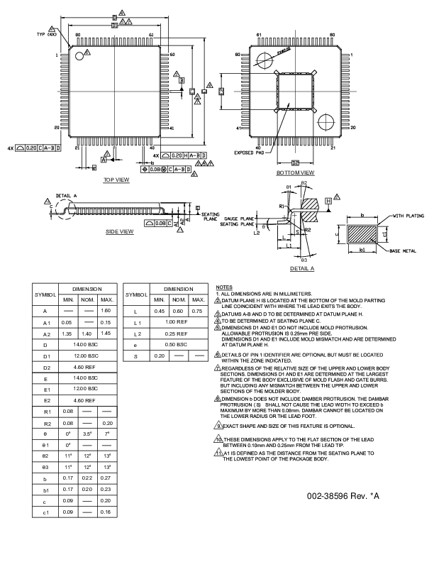
Figure 14.
E-LQFP-64, 10x10x1.6 mm
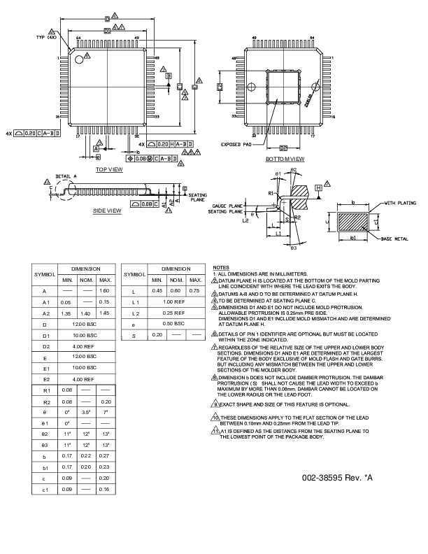
Figure 15.
VQFN-64, 8x8x0.9 mm
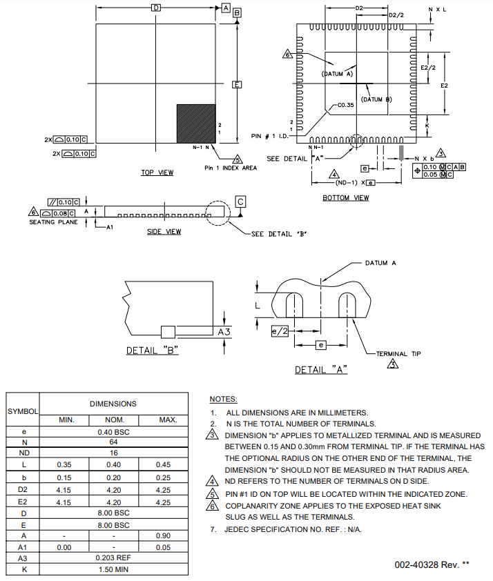
Figure 16.
E-LQFP-48, 7x7x1.6 mm
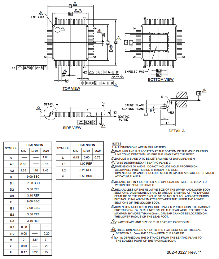
Figure 17.
VQFN-48, 6x6x0.9 mm
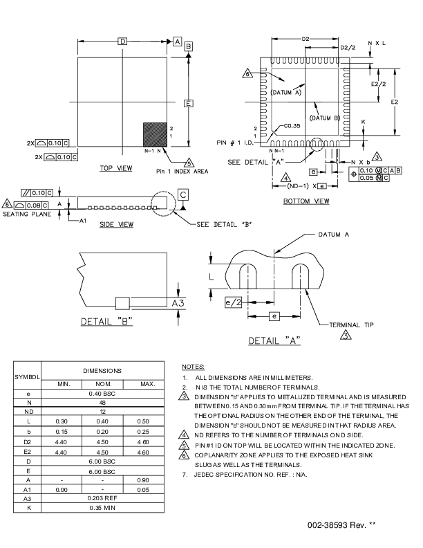
Errata
This section describes the errata for the
PSOC™ Control C3
MCU product line. Details include errata trigger conditions, scope of impact, available workarounds, and silicon revision applicability. For more details, contact
Infineon support
.
Part numbers affected
Part number | Device characteristics |
|---|---|
All | PSOC™ Control C3 MCU product line |
PSOC™ Control C3 qualification status
Production silicon
PSOC™ Control C3 errata summary
The following table defines the errata applicability of available product line devices.
Note:
Click on any item entry to view its description.
| |
|---|---|
Problem definition | FLL may not start properly after waking up from Deep Sleep in ULP (VCCD = 0.9 V) and MF (VCCD = 1.0 V) power profiles. |
Parameters affected | FLL output frequency. |
Trigger condition | Deep Sleep wake up in ULP and MF power profiles with FLL enabled. |
Scope of impact | FLL operation in ULP and MF modes after wake up from Deep Sleep. |
Workaround | Set the SRSS.PWR_TRIM_WAKE_CTL register to 1 after selecting ULP or MF power profiles. |
Fix status | Fix planned. |
| |
|---|---|
Problem definition | Device is permanently non-responsive if Flash row 0 contains uncorrectable ECC errors. |
Parameters affected | Device cannot be used. |
Trigger conditions |
|
Scope of impact | Device becomes permanently non-responsive |
Workaround |
|
Fix status | Fix planned. |
| |
|---|---|
Problem definition | For VDDD < 2.3 V, Deep Sleep wake-up operation may lead to a system reset. |
Parameters affected | MCU wake up from Deep Sleep or Deep Sleep-RAM modes. |
Trigger condition | When device VDDD < 2.3 V, device is in Deep Sleep and a wake-up interrupt is triggered. |
Scope of impact | Device is reset. |
Workaround | Use VDDD ≥ 2.3 V when using Deep Sleep and Deep Sleep-RAM modes. |
Fix status | Fix not planned. |
| |
|---|---|
Problem definition | If LPComp interrupt is configured as wake up source for Deep Sleep-RAM or Deep Sleep-OFF mode, MCU cannot wake up when LPComp interrupt is asserted. |
Parameters affected | MCU wake up from Deep Sleep-RAM or Deep Sleep-OFF modes. |
Trigger condition | LPComp interrupt event for wake up from Deep Sleep-RAM or Deep Sleep-OFF modes. |
Scope of impact | LPComp peripheral cannot be used as a wakeup source for Deep Sleep-RAM or Deep Sleep-OFF modes. |
Workaround | Use Deep Sleep mode instead of Deep Sleep-RAM or Deep Sleep-OFF. |
Fix status | Fix not planned. |
| |
|---|---|
Problem definition | SCB: In I2C slave mode, the TXFIFO underflow interrupt is falsely triggered if an external master sends an ACK for the final byte read operation before the STOP or RESTART condition. |
Parameters affected | TXFIFO underflow interrupt during I2C slave transmit operation. |
Trigger condition | Triggered when an external I2C master sends an ACK for the final byte read transaction before STOP or RESTART. |
Scope of impact | SCB in I2C slave mode during normal read operation. |
Workaround | External I2C master needs to send a NACK for the last read operation before STOP or RESTART. |
Fix status | Fix not planned. |
| |
|---|---|
Problem definition | If SCB is configured as SPI master TI mode, transmit FIFO is configured with 8 bits per FIFO data element (MEM_WIDTH=0), and transmit data frame is configured for 5 bits (TX_CTRL width=4), TX_CTRL.MSB_FIRST=1, the data output is incorrect. |
Parameters affected | SPI data output is incorrect. |
Trigger condition | SCB is configured as SPI master TI mode with an 8-bit transmit FIFO data element and TX_WDTH=4. |
Scope of impact | Impacted in one specific configuration detailed above. |
Workaround | None. |
Fix status | Fix not planned. |
| |
|---|---|
Problem definition | MCWDT_LOWER_LIMIT.WDT_LOWER_LIMIT0 is only supported for the first two 16-bit counters. It is disabled when the third 32-bit counter is cascaded (MCWDT_CONFIG.WDT_CASCADE1_2 == 1). |
Parameters affected | Cascading of MCWDT counters beyond the first two 16-bit counters. |
Trigger condition | When MCWDT_CONFIG.WDT_CASCADE1_2 == 1. |
Scope of impact | MCWDT_LOWER_LIMIT.WDT_LOWER_LIMIT0 is only supported for the first two 16-bit counters. |
Workaround | None. |
Fix status | Fix not planned. |
| |
|---|---|
Problem definition | In timer mode, value of TCPWM0_GRPx_CNTx_CTRL.UP_DOWN_MODE may change when the counter is stopped. |
Parameters affected | Counter direction in timer mode. |
Trigger condition | After counter is stopped and then started again in timer mode, direction may change. |
Scope of impact | TCPWM in timer mode. |
Workaround | When the counter is stopped, update the TCPWM0_GRPx_CNTx_CTRL.UP_DOWN_MODE value as per intended direction before restarting the counter. |
Fix status | Fix not planned. |
| |
|---|---|
Problem definition | The KILL_STATUS bit is asserted falsely when the counter is not running. |
Parameters affected | Only the KILL_STATUS flag bit visibility in software. PWM outputs are not impacted. |
Trigger condition | Triggered when kill is enabled and the counter is not running due to:
|
Scope of impact | Only when the counter is not running. |
Workaround | Ignore the KILL_STATUS in the software when the counter is not running (TCPWM0_GRPx_CNTx_STATUS.RUNNING = 0). |
Fix status | Fix not planned. |
| |
|---|---|
Problem definition | PWM TC synchronous DT kill (PWM_TC_SYNC_KILL_DT=1) is not available in HRPWM mode. |
Parameters affected | TC synchronous DT kill feature availability in HRPWM mode. |
Trigger condition | When dead time is defined to be non-zero, PWM_TC_SYNC_KILL_DT=1 and HRPWM = 1. |
Scope of impact | If dead-time is defined to be non-zero, the HRPWM line_out does not wait for dead-time after TC event when killed in PWM_TC_SYNC_KILL_DT mode. |
Workaround | None. |
Fix status | Fix not planned. |
| |
|---|---|
Problem definition | CC0 match not generated at reload for count down mode when HRPWM duty cycle is set to 100%. |
Parameters affected | HRPWM duty cycle |
Trigger condition | HRPWM in count down mode (TCPWM0_GRP0_CNTx_CTRL.UP_DOWN_MODE=1) and duty set to 100% (CC0 = period). |
Scope of impact | HRPWM output in TCPWM0_GRP0_CNTx_CTRL.UP_DOWN_MODE=1 does not generate 100% duty cycle after reload when CC0 = period. |
Workaround | Program CC0 to period-2 and CC0_BUFF to period and enable compare swap. |
Fix status | Fix not planned. |
Acronyms
Acronym | Description |
|---|---|
ADC | analog-to-digital converter |
AES | advanced encryption standard |
AMUX | analog multiplexer |
BLDC | brushless direct current |
BOD | brown-out detect |
CAN | controller area network |
CORDIC | coordinate rotation digital computer |
CSV | clock supervision |
DAC | digital to analog converter |
DFU | device firmware upgrade |
DSI | digital signal interconnect |
DSP | digital signal processor |
DMA | direct memory access |
ECC | error correcting code |
ECO | external crystal oscillators |
ETB | embedded trace buffer |
ETM | embedded trace macrocell |
FET | field effect transistor |
FIFO | first in, first out |
FOC | field-oriented control |
FPU | floating point unit |
GPIO | general-purpose input/output |
HPPASS | high-performance programmable analog subsystem |
HRPWM | high-resolution pulse width modulator |
HSIOM | high-speed I/O matrix |
I-cache | instruction-cache |
I2C | inter-integrated circuit |
IHO | internal high-speed oscillator |
ILO | low-speed oscillator |
IMO | internal main oscillator |
IPC | inter-processor communication |
IRQ | interrupt request |
ISR | interrupt service routine |
LPComp | low-power comparator |
LUT | lookup table |
LVD | low-voltage detection |
LVTTL | low-voltage transistor-transistor logic |
MCWDT | multi-counter watchdog timer |
MPU | memory protection unit |
NVIC | nested vectored interrupt controller |
PAL | programmable array logic |
PLD | programmable logic device |
PLL | phase-locked loops |
POR | power-on reset |
ROM | read-only memory |
RSA | rivest-shamir-adleman, a public-key cryptography algorithm |
RTC | real-time clock |
RWW | read-while-write |
S/H | sample/hold |
SAR | successive approximation register |
SAU | secure attribution unit |
SCB | serial communication blocks |
SHA | secure hash algorithm |
SPI | serial peripheral interface |
SRAM | static random access memory |
SRSS | system resources subsystem |
TCPWM | timer/counter pulse-width modulator |
TRNG | true random number generator |
UART | universal asynchronous transmitter receiver |
WCO | watch crystal oscillator |
WIC | wakeup interrupt controller |
XRES | external reset input pin |
Document conventions
Units of measure
Symbol | Unit of measure |
|---|---|
°C | degree Celsius |
KB | 1024 bytes |
kHz | kilohertz |
Mbps | megabits per second |
Msps | million samples per second |
MHz | megahertz |
ns | nanosecond |
% | percent |
V | volt |
Revision history
Document version | Date of release | Description of changes |
|---|---|---|
** | 2022-09-26 | Initial release |
*A | 2023-08-30 | Updated the document title Added the gxg1730181873132.html#mfy1698739677971 section Added the Low-power comparator (LPComp) section Updated the Block functional description section Updated TCPWM for HRPWM support Added the gxg1730181873132.html#lqc1681475602142 section Added the Electrical specifications section |
*B | 2024-01-25 | Updated the document title Added short product description Updated the Features section Updated the Potential applications section Updated the Description section Added chip symbol and marketing block diagram Added the Introduction section Updated Figure 1 Added the Chip-level functional description section Updated the Block functional description (previously "Functional description") Updated the gxg1730181873132.html#mfy1698739677971 section Updated the Electrical specifications section Added the gxg1730181873132.html#bcm1697083377157 section Added the Errata section |
*C | 2024-03-11 | Added additional package images on first page Updated the Electrical specifications section Updated the gxg1730181873132.html#lqc1681475602142 section Updated the gxg1730181873132.html#bcm1697083377157 section |
*D | 2024-05-29 | Updated package images on first page Updated Figure 1 Updated the Detailed features section Added the Device firmware update (DFU) section Updated the gxg1730181873132.html#mfy1698739677971 section Updated the Electrical specifications section Updated the gxg1730181873132.html#bcm1697083377157 section Updated the Errata section |
*E | 2024-12-20 | Updated image and features on first page Updated Figure 1 Updated the Detailed features section Updated the Chip-level functional description section Updated the Clock system section Updated the 12-bit SAR analog-to-digital converter (ADC) section Updated the Serial communication block (SCB) section Updated the Trigger multiplexer (Trigger MUX) section Updated the Device firmware update (DFU) section Added the Serial wire JTAG debug port/Embedded trace macrocell section Updated the gxg1730181873132.html#mfy1698739677971 section Updated the GPIO alternate functions tables section Updated the Electrical specifications section Updated the gxg1730181873132.html#lqc1681475602142 section Updated the gxg1730181873132.html#bcm1697083377157 section Updated the Errata section Publish to web |
*F | 2025-04-15 | Updated features on first page Updated the Device firmware update (DFU) section Updated the Serial wire JTAG debug port/Embedded trace macrocell section Updated the gxg1730181873132.html#mfy1698739677971 section Updated the GPIO alternate functions tables section Updated the gxg1730181873132.html#bcm1697083377157 section Updated the Document conventions section |
Trademarks
PSOC™, formerly known as PSoC™, is a trademark of Infineon Technologies. Any references to PSoC™ in this document or others shall be deemed to refer to PSOC™.