AN-G2-ASSEMBLY Assembly instructions for the HybridPACK™ Drive G2 power module
About this document
Scope and purpose
This application note describes the recommended process for assembling the HybridPACK™ Drive G2 power module into the inverter system and also includes the integration of differential Hall-based phase current sensors from Swoboda Technologies
10
.
This application note also provides the best practices on how to assemble the HybridPACK™ Drive G2 modules to get a robust system design.
Moreover, this application note cannot cover every type of application, condition, and system combination. Therefore, it cannot replace a detailed evaluation and examination by your technical divisions of the suitability for the targeted applications and mounting processes.
In addition, the maximum permissible values in the corresponding product datasheet are absolute limits, which generally, even for short times, may not be exceeded as this may lead to destruction, pre-damage, and accelerated aging of the component.
The application note will, therefore, under no circumstances become part of any supplier agreed warranty, unless the supply agreement determines otherwise in writing.
Intended audience
This document is primarily intended for engineers and operators involved in the assembly of the HybridPACK™ Drive G2 power module into power electronics systems.
The semiconductor power modules are electrostatic components. Therefore, follow appropriate electrostatic discharge (ESD) safety instructions at all time during the assembly processes.
General information
The HybridPACK™ Drive G2 power module (see
Figure 1
) is the next generation of well-established HybridPACK™ Drive power modules and has a compatible mechanical outline to support a modular and scalable inverter system approach.
HybridPACK™ Drive G2 modules come with an improved frame material for enabling higher temperatures and currents. The guiding elements for power module positioning and alignment are optimized for fully automated assembly lines. The module baseplate is a PinFin baseplate for direct fluid-cooled systems and support the highest power densities.
Signal pins are optimized press-fit pins, which are qualified according to the following latest standards:
IPC-9797:May2020, "Press-Fit Standard for Automotive Requirements"
IEC 60352-5:2020, "Solderless connections"
The gate driver boards can be fixed by the heat stake process or alternatively, by self-tapping screws. The power module is also prepared for coreless phase current sensors (see
Figure 2
). The power module has a pocket in the frame and a slotted AC tab, which enables differential Hall sensors for precise measurement of the motor phase currents. For details for the sensor integration, see Section
10
.
Figure 1. HybridPACK™ Drive G2 power module
Figure 2. Differential Hall phase current sensors (CSM510HP2S or CSM510HP2D) for the HybridPACK™ Drive G2 power modules. For detailed information, see the product website [10]
shows the scope of this application note for the following products:
Type designation | Product description | Remarks | Status |
|---|---|---|---|
FSxxxRxxA7Pxyyy | HybridPACK™ Drive G2 IGBT module | – | In production |
FSxxxxRxxA8Pxyyy | HybridPACK™ Drive G2 enhanced IGBT module | – | In production |
FSxxMRxxA8MAxyyy | HybridPACK™ Drive G2 SiC MOSFET module | – | In production |
FSxxxRxxA7FUxxyyy | HybridPACK™ Drive G2 Si/SiC Fusion module | – | In production |
CSM510HP2S | Differential Hall phase current sensor module with single-ended output | To order this product, see 10 Samples are available under Infineon order number SP005861812 | For product status, see 10 |
CSM510HP2D | Differential Hall phase current sensor module with differential output | To order this product, see 10 Samples are available under Infineon order number SP005861817 | For product status, see 10 |
If your product is not listed, contact Infineon support or your local sales representative.
Power module mounting
Datasheet drawings specify the power module at the state of delivery (before the assembly) in case not otherwise specified. Minor deformations on the product will occur during the assembly processes. To ensure a seamless mounting, it is recommended to follow the mounting order. More details about the process are described in the later sections.
Align PCB (gate driver boards) to the power module. See Section 3
If phase current sensors are implemented, see Section 10 for detailed information
Press in the PCB. See Section 4
Prepare the cooling system with the sealing ring and attach the power module to the cooling system. See Section 5
Fix the module baseplate on the cooler by screws. See Section 6
Fix the PCB on the power module by heat stake process or alternatively by screws. See Section 7
Connect the module power tabs to the busbar, capacitor, etc. See Section 8
Module alignment and x,y guiding holes
HybridPACK™ Drive G2 power modules come with a new coordinate reference system, which is defined by two 4 mm holes in the baseplate. The x-hole is at the side of the six DC power tabs and the slotted y-hole is at the side of the three AC power tabs. The holes are designed to mate with alignment domes that can be implemented by the customer.
You can use one of the following options:
In cooler/inverter housing (see Figure 4 B)
Note that you can use either option A or B; you cannot use both the options together.
Option 1 has the alignment domes only in the manufacturing equipment and provides the lowest system BOM cost. Option 2 requires you to adjust the press-tool; see
Figure 6
. The alignment dome (noted in Element 1 of
Figure 6
) must be replaced by a hollow cylinder with a 4.1 mm inner diameter to avoid collisions.
Figure 3. Reference coordinate system defined by x-hole and slotted y-hole in the baseplate. See the product datasheet 2 for detailed information
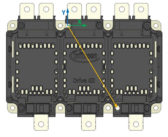
Figure 4. Principal view: Alignment of the power module, cooler, and PCB by alignment domes in handling and press-tools (a) or by alignment domes in cooler/inverter housing (b). The alignment domes are indicated by light blue color. For detailed information about current sensor alignment, see Section
10Press-fit signal contacts
PCB requirements
The press-fit signal pin technology used in HybridPACK™ Drive G2 power modules is designed for standard FR4 printed circuit boards (PCBs) with immersion tin plating. This technology is qualified according the following standards:
Is qualified according to IPC 9797:May2020, "Press-Fit Standard for Automotive Requirements"
Passes the conditions and criteria according to IEC 60352-5:2020
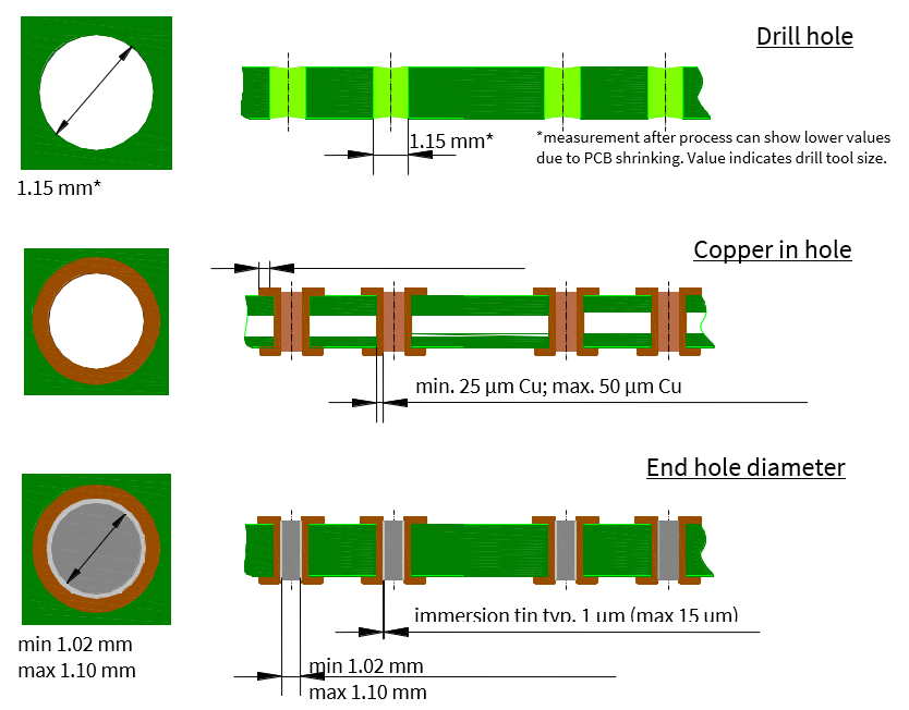
The PCB material must be compliant with IEC 60249-2-4 or IEC 60249-2-5 for double-sided PCBs and IEC 60249-2-11 or IEC 60249-2-12 for multilayer PCBs. The requirements for the PCB are shown in
Table 2
. If the requirements are not met, there is risk of a not gas-tight signal pin connection or of damage to pin and PCB via.
Note that press-fit hole specifications are valid only for assembled PCBs. In the case of unassembled PCBs (e.g., for testing purposes), it is recommended to perform a standard reflow solder process before starting the power module assembly process.
No. | Description | Unit | Min. | Typ. | Max. | Notes/conditions and known errors |
|---|---|---|---|---|---|---|
1 | Drill tool diameter | mm | 1.12 | 1.15 | – | Wrong drill tool applied. Clearly specify the press-fit hole positions and required drill tool size to the PCB manufacturer |
2 | Copper thickness in the hole | μm | 25 | – | 50 | If the via metallization is lower than the specification, there is risk of a damaged/cracked via |
3 | End-hole diameter | mm | 1.02 | – | 1.10 | End-hole diameters lower than the specification may lead to increased press-in forces and may damage the pins. Larger holes than the specification may lead to low press-in forces and can cause not gas-tight connections |
4 | Copper thickness of conductors | μm | 35 | 70 105 | 400 | – |
5 | Hole to hole pattern tolerance | μm | – | – | ±100 | In typical PCB manufacturing, the hole-to-hole pattern is lower than ±80 μm |
6 | Recommended PCB thickness | mm | – | 1.6 | – | Target value with ±10% tolerance for thickness |
7 | Metallization of circuit board | – | Immersion tin (Sn chemically) | Immersion tin has typically 1 μm to 5 μm metallization in the hole. Other metallization types should be avoided as these can lead to strong deviation in press-in forces. For example, HAL leadless shows high variations in press-in forces and has the risk of a not gas-tight pin connection, which can fail over the application lifetime. PCB with ENIG (Ni Au) plating can lead to increased press-in forces due to hard surfaces. OSP-plated PCBs were not considered during the development phase. Surfaces other than Immersion Tin will not be considered at Infineon module qualification tests | ||
8 | Metallization of pin | – | Ni/Sn (galvanic) | The Sn plated pin with nickel under layer avoids potential whisker growth out of the upper galvanic tin layer | ||
Note that the PCB press-fit holes should not be specified just by the finished end-hole diameter. The risk is that the wrong processes are applied by the PCB manufacturer. Ensure that you provide your PCB manufacturer the information that all holes for the signal pins must be manufactured according to
Table 2
. As PCB design tools typically do not differentiate between normal and press-fit holes, it is a well-known workaround to use a unique hole size, for example, 1.06 mm in the PCB design for all press-fit holes. In this case, the press-fit holes are separate in the NC drill files. Therefore, the PCB manufacturer knows exactly the positions where to apply the specification according to
Table 2
.
A structure of a PCB according to the specification in
Table 2
is illustrated in
Figure 5
. The hole in the PCB is drilled with a drill tool size of 1.15 mm. It is normal that the PCB material shrinks after drilling. Therefore, the hole size shown with 1.15 mm should not be taken as a check gauge after drilling; you should take this as an illustration for understanding the PCB stack.
Later in the process, the holes will be plated. Holes must have a minimum 25 μm copper in the hole. Otherwise, press-in forces may damage/crack the via. According to experience, larger annular rings are typically more robust to mechanical forces. Therefore, large annular rings (e.g., 0.5 mm) should be used wherever possible in the design.
The metallization/plating in the holes must be manufactured in an immersion tin (i.e., chemical tin) process. This process is known to generate uniform layer thicknesses (typically about 1 μm) and ensures correct press-in forces as well as an appropriate contact surface for achieving gas-tight press-fit connections.
Figure 5. Structure of a PCB according to the specification in Table 2
PCB footprint recommendations
PCB footprint typically depends on PCB manufacturing processes and customer-specific design rules. Table 3 shows a few best practices and gives a starting point for your system design.
No | Type | PCB implementation |
|---|---|---|
1 | X hole | Hole at 0/0 mm position End-hole diameter: 4.10 mm ±0.1 Optional: Plated hole with 4.7 mm annular ring
diameter |
2 | Y hole | Hole at 49.274/-82 mm position End-hole diameter: 4.10 mm ±0.1 slotted length 4.5 mm Slot rotation (59° top view) Optional: Plated hole with 5.1 mm annular ring
diameter |
3 | Signal press-fit pin holes | See Table 2 |
4 | Components keepout around press-fit pins | Uncritical packages like SO, TSSOP, QFP, or not safety-relevant SMD resistors: ≥3 mm radius from the hole center Others: ≥4 mm radius from the hole center |
5 | PCB heat stake fixing 1 | 6x holes at positions: (HS1: -46.2/0 mm; HS3: 31.47/0 mm; HS4: 78.8/0mm) (HS5: 78.8/-82 mm; HS7: 1.13/-82 mm; HS8: -46.2/-82 mm) End hole diameter: 3.60 mm ±0.1 mm Optional: Plated hole with annular ring diameter
top layer 6.6 mm; mid layer 4.2 mm; bottom layer 7.0
mm |
6 | Optional PCB screw fixing | Optional 6x holes:
End-hole
diameter: 3.60 mm �±0.1 mm Optional: Plated hole with annular ring diameter
top layer 7.0 mm; mid layer 4.2 mm; bottom layer 6.6
mm |
Press-tools
This section describes a sample press tool that can be adapted to project-specific needs such as PCB assembly locations and maximum height of other PCB parts to avoid mechanical collisions during the press-in process. The press tool is made of two parts and changeable alignment domes (see
Figure 6
).
A mechanical drawing of the sample press-tools is shown in
Figure 7
and
Figure 10
. A 3D step model can be obtained from Infineon Technologies on request.
The press tool can be used in a simple toggle lever press for engineering purpose or in a controlled press-machine for serial production (for example, see
3
).
Figure 6. Press-tool (principle view)
The top tool implements:
Changeable X/Y alignment domes that provide a poka-yoke that no wrong assembly orientation of power module and press tools are possible (two alignment domes)
Punch for the signal pins designed as hollow cylinders ('n' times for all 'n' signal pins)
Optional punch for the phase current sensor (three times)
Distance keeper (six times at heat stake dome position), which simplifies the press-stop criteria
The elements 2 to 4 are in the same common zone. The top tool height (height of the cylinders) must be adjusted according to the maximum PCB assembly height.
The alignment domes are implemented in the sample tool as changeable inserts. In case of equipment crash or other incidents, the domes can be easily replaced (M4x18 DIN 7991) in the service interval without the need of a completely new production tool.
The bottom tool implements the following:
Locating the surface for the power module baseplate
Groove to protect the PinFin baseplate structure from scratches and damage
Changeable guide element for power module positioning in the bottom tool
Poka-yoke element to avoid incorrect assembly orientation. The element can be designed also with a tactile sensor which locks the press-machine operation
Drill holes for X/Y alignment domes of the top press tool
The material and/or plating of the bottom part of the tool must be selected to avoid scratches and damage of the baseplate sealing area during the press-in process.
Press tool IGBT signal pinning
Figure 7. Sample press tool IGBT signal pinning (top tool)
Infineon drawing number: W00210353
Edges: ISO 13715; tolerance: ISO 2768 – mK; surface: EN ISO 1302; material: 1.4301 (V2A)
Press tool SiC MOSFET signal pinning
Figure 8. Sample press tool SiC MOSFET signal pinning (top tool)
Infineon drawing number: W00208361
Edges: ISO 13715; tolerance: ISO 2768 – mK; surface: EN ISO 1302; material: 1.4301 (V2A)
Press tool Si/SiC Fusion signal pinning
Figure 9. Sample press tool Si/SiC Fusion signal pinning (top tool)
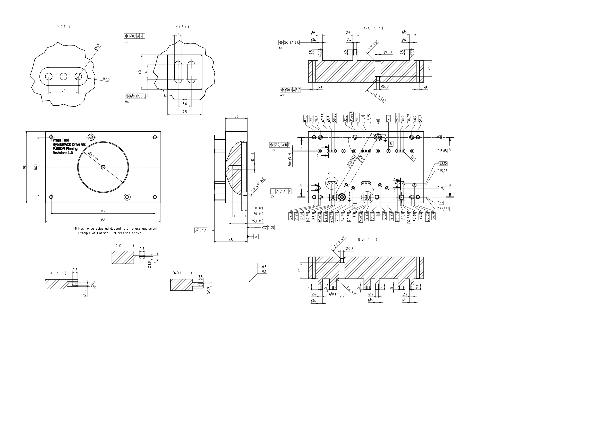
Infineon drawing number: W00273471
Edges: ISO 13715; tolerance: ISO 2768 – mK; surface: EN ISO 1302; material: 1.4301 (V2A)
Bottom press tool and alignment dome (all versions)
Figure 10. Sample press tool (bottom tool)
Infineon drawing number: W00209424 (alignment element W00209432)
Edges: ISO 13715; tolerance: ISO 2768 – mK; surface: EN ISO 1302;
Material bottom tool: 1.4301 (V2A)
Material alignment nobs: ABS plastic
Figure 11. X/Y alignment domes of the sample press tool (two times for the top tool). The alignment domes can be fixed by metric M4x18 DIN7991 screws in the top tool
Infineon drawing number: W00209433
Edges: ISO 13715; tolerance: ISO 2768 – mK; surface: EN ISO 1302; material: 1.4301 (V2A)
Press-in process
The press-in process is recommended with a controlled force-distance method for serial production. For testing under laboratory conditions, a manual toggle-press also typically gives good results.
shows an example of a HybridPACK™ Drive G2 press-in process with a typical PCB according to
Table 2
. The PCB thickness in this test was 1.6 mm (±10%).
Note that the press-in equipment is designed for the expected high forces. During the press-in process, the bottom and top press-tool must be parallel to each other and should be mechanically fixed without tilt.
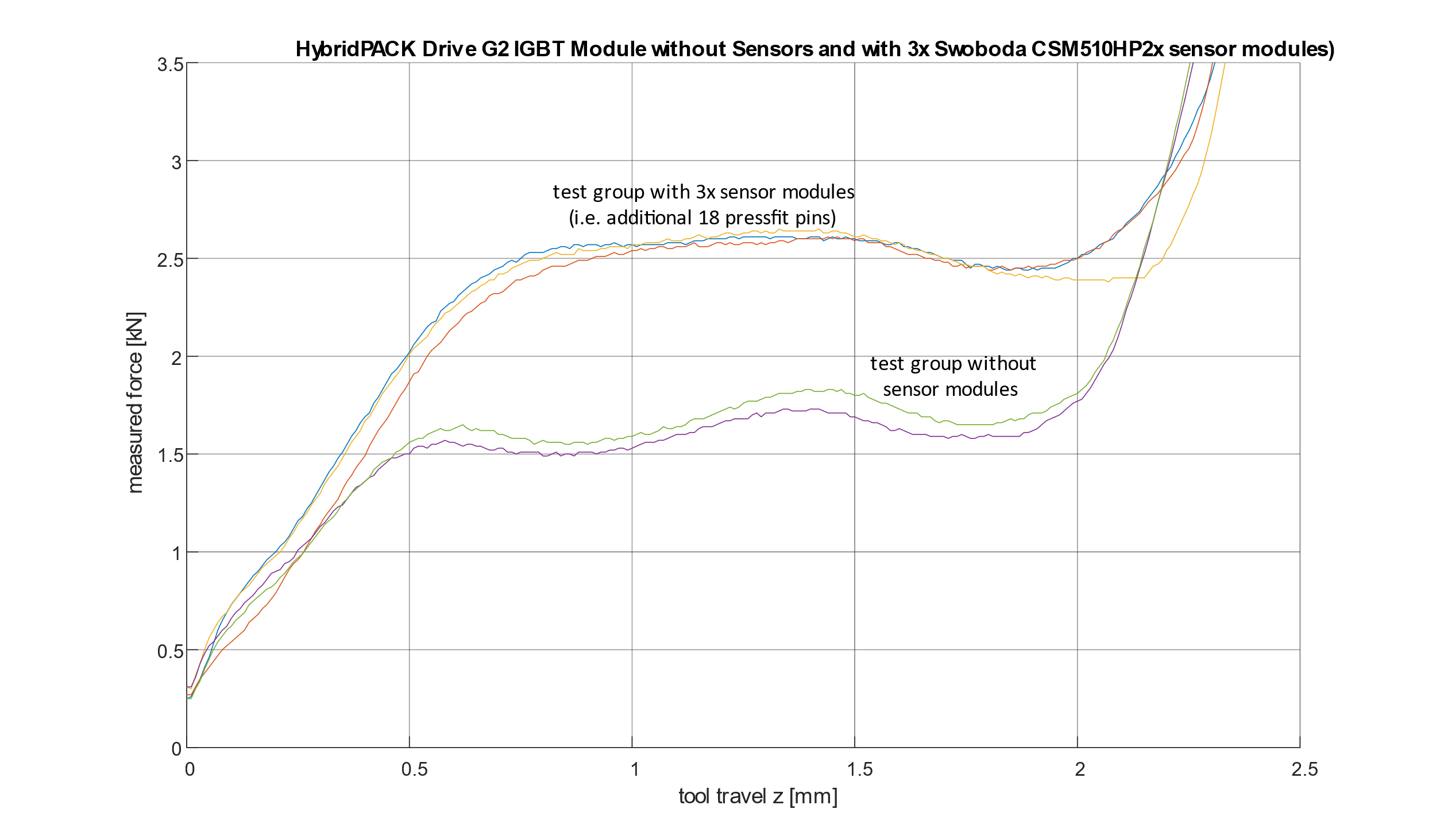
Figure 12. Typical way-force press-in diagram with HybridPACK™ Drive G2 module. The power module in this example is an IGBT module with 27 signal pins. The Swoboda CSM510HP2S or CSM510HP2D sensor has six signal pins per sensor and three sensors are used per system
No | Description | Unit | Min. | Typ. | Max. | Notes/conditions |
|---|---|---|---|---|---|---|
1 | Press-in speed | mm/s | 0.4 | 2 .. 4 | 8 | During the press-in process, it is not recommended to come under the minimum speed. The maximum press-in speed is typically limited by press equipment limitations |
2.1 | Max allowed press force on module (power module with three sensor modules CSM510HP2S or CSM510HP2D) | kN | – | 2 .. 3 | 3.5 | Exceeding the maximum allowed force can lead to increased signal pin mechanical stress and can also damage the frame and baseplate of the power module |
2.2 | Max allowed press force on module Bare module (no sensors) | kN | – | 1.2 .. 2 | 3.0 | Exceeding the maximum allowed force can lead to increased signal pin mechanical stress and can also damage the frame and baseplate of the power module. |
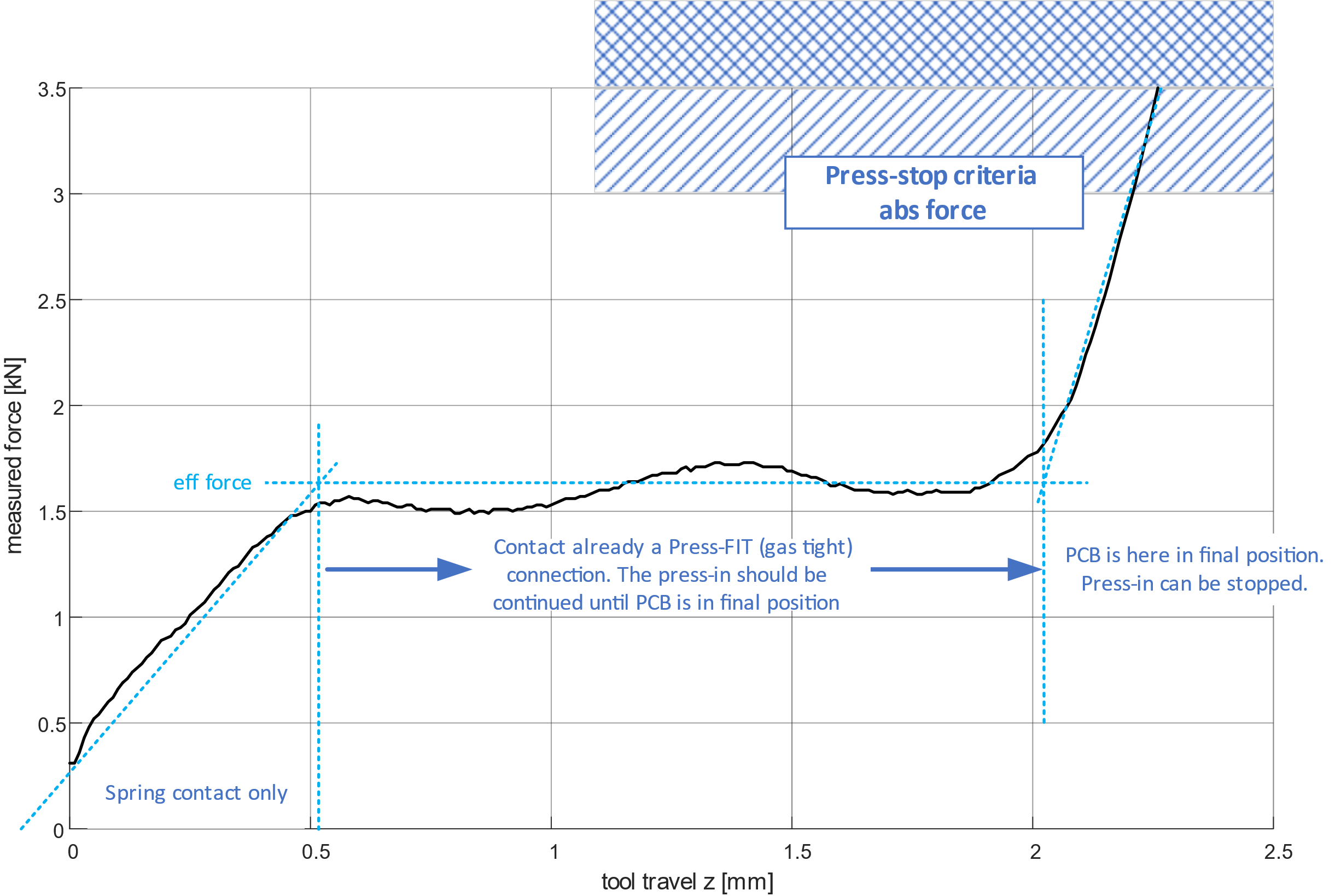
shows typical process parameters. At the beginning, the pin slides into the PCB holes and gets deformed. In the beginning, the contact is a spring contact only. The pin itself will limit the effective force to prevent damage in PCB vias. At the end of the process, the PCB will attach to the power module frame and the force will be introduced into the frame. At this point, the process is already finished and the press-in can be stopped. Some press machines provide the option to stop the process by slope changing points (dF criteria). Such a stop-criteria is the most advanced and can be applied, but is not mandatory for HybridPACK™ Drive G2 power modules. For qualification tests at Infineon Technologies where a PCB assembly was required, a press-stop criteria by absolute force according to
Table 4
is applied.
Figure 13. Typical way-force press-in diagram with indication of the typical process parameters
Power module cooling system
The module power losses must be dissipated in order not to exceed the maximum permissible operating temperature specified in the datasheet
2
. Therefore, the design of a cooling system/heat sink is of great importance.
The HybridPACK™ Drive G2 module has a PinFin array on the baseplate, which makes liquid cooling very effective. The baseplate is made of copper (Cu) material with nickel (Ni) plating. The PinFin structure is suitable for cooling fluids like water and ethylene glycol mixture. The fluid mixture also requires an appropriate corrosion protection; see
Cooling fluid
for details.
During the assembly process, avoid damage to the nickel plating or mechanical deformation of the PinFin structure as well as contamination, scratches, or other damages in the sealing area.
Reference cooler design
The cooler design has a great impact on the overall cooling performance, which means the combination of thermal resistance/impedance, pressure drop, and cooling flow rate. Thus, for all of these thermal-related product specifications, a reference cooling system is required where the given specification values are valid.
The cooler can be designed differently if other tradeoffs of thermal resistance/impedance, pressure drop, and flow rates must be achieved. Therefore, the reference cooler should be regarded as a design example, where the values from the corresponding product datasheet can be achieved.
Figure 14. Reference cooler design for HybridPACK™™ Drive G2 with PinFin cooling structure
Infineon drawing number: W00203206; DIN ISO 13715; ISO 2768-mK; DIN EN ISO1302; AlMgSi0.5
The 2x guiding holes for the reference system are drawn as through-holes in the example but can be adjusted to project-specific needs like 8 mm depth blind holes or similar.
Consider the following requirements when designs other than the reference cooler is used:
Roughness of the cooler: ≤ RZ25 (DIN EN ISO 1302) in area of the sealing
Cooler flatness at the module area: ≤ 50 µm
Exceeding these requirements may lead to damage of the power module.
The cooler material should be AlMgSi0.5 or alternative, which is compatible to copper baseplate with nickel plating and can withstand the mechanical stress required from a specific customer application.
For prototyping purposes, the reference cooler with a matching sealing ring can be ordered from
Hitex GmbH
.
Plastic coolers are already demonstrated for HybridPACK™ Drive Generation 1 products by
6
,
5
. Such coolers can also be applied to HybridPACK™ Drive G2 power modules.
Sealing ring recommendations
The power module baseplate is designed with a flat region of 6.5 mm surrounding the entire PinFin area, which is called the "sealing area".
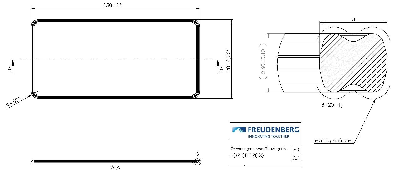
Several power module qualification tests like power cycling tests require the assembly on a cooler. For these tests, OR-SF-19023 sample sealing rings from Freudenberg Sealing Technologies
4
were applied. This sealing ring type is already a known design from HybridPACK™ Drive power modules of the first-generation where all reliability tests from AQG324 were finished with PASS result. Nevertheless, it is necessary to perform a system qualification test (e.g., according to LV124) to ensure that the final system design and final assembly processes meet the project-specific application needs. The system qualification is also mandatory if other sealing rings and/or coolers must be used in applications.
Figure 15. OR-SF-19023 sealing ring from Freudenberg Sealing Technologies
Depending on system assembly processes, the so-called assembly nobs at the sealing rings can be useful. Such a design is shown in
Figure 16
. Besides the assembly nob feature, it provides the same sealing characteristics.
Figure 16. OR-SF-21004 sealing ring from Freudenberg Sealing Technologies
An incorrect placement of the sealing ring in the cooler grove can lead to deformation of the power module baseplate and fluid leakage as a consequence. Note that repair/rework after a wrong assembly is not possible.
For prototyping purposes, the reference cooler with a matching sealing ring can be ordered from
Hitex GmbH
.
Cooling fluid
A general recommendation for a specific cooling fluid cannot be provided, because the power module is only one single part in the entire cooling system. Consider the following at the system supplier to find the appropriate coolant fluid:
Coolant fluid with its corrosion protection must be compatible with the aluminum alloy of the cooler material and the nickel-overplated copper baseplate from the power module
Other parts in the coolant system must be compatible to the fluid type (e.g., Zn screws and chrome parts are typically not allowed in the cooling system)
The fluid mixture must provide enough antifreeze for the application conditions and must avoid freezing events of the fluid. Freezing fluid will lead to plastic deformation of the power module baseplate and will lead to fluid leakage and/or isolation failure consequently
For power module tests at Infineon where cooling is required (e.g., thermal characterization, power cycling tests), typically BASF Glysantin G30 with an organic-acid-technology (OAT) silicate-free corrosion protection is applied.
Baseplate mounting on the cooler
The power module baseplate is designed to be fixed on the cooling system by means of screws. Using the correct screw types, torques, screw orders, and module clamping is essential to avoid damage of the power module during the assembly steps.
Baseplate mounting with metric screw types
In case of power module baseplate mounting by metric screws, consider the following from
Baseplate mounting with metric screw types
.
No. | Description | Unit | Min. | Typ. | Max. | Notes/conditions |
|---|---|---|---|---|---|---|
1 | Metric screw type (recommended) | – | – | ISO 7380-2 A2 (TX) M4x10 | – | Recommended metric screw |
1.1 | Metric screw type (option) | – | – | ISO 4762 (screw) ISO 7090 (washer) M4x10 | – | Due to production complexity/cost only for lab testing recommended |
2 | Mounting torque | Nm | 1.8 | 2.0 | 2.2 | – |
3 | Maximum mounting speed | rpm | – | – | 400 | – |
4 | Effective length of screw in cooler | mm | 6 | – | – | AlMgSi0.5 cooler material. Typical M4x10 screws are used |
5 | Screw order | – | – | According to the section Screw order and module clamping during baseplate screw process | – | Correct screw order is mandatory |
6 | Module clamping during screw process | kN | – | 2 According to Screw order and module clamping during baseplate screw process | – | Clamping or multi-step mounting. See Screw order and module clamping during baseplate screw process |
Baseplate mounting by self-tapping screws
Self-tapping screws avoid drilling and thread cutting as well as corresponding cleaning processes of the cooler/inverter housings. Therefore, it leads to significant reduction in cost and process time at high production volumes. Furthermore, such self-tapping screws are known to be extremely rugged during vibration stress.
No. | Description | Unit | Min. | Typ. | Max. | Notes/conditions |
|---|---|---|---|---|---|---|
1 | Self-tapping screw type (recommended) | – | – | EJOT ALtracs Plus WN5152 AP 40x12/10 | – | Recommended screw |
2 | Mounting torque M eff | Nm | 1.6 | 1.8 | 2.0 | Approx. Mw = 2 Nm torque is required for the self-tapping. This torque is not effective for the mounting force Ft. Self-tapping force strongly depends on the cooler material |
3 | Recommended mounting speed | rpm | 400 | – | 600 | Lower than 200 rpm is not recommended |
4 | Screw holes in cooler | – | – | See Figure 17 | – | Self-tapping screws should not be used in standard M4 threads |
5 | Screw order | – | – | See Screw order and module clamping during baseplate screw process | – | Screw order crosswise from inside to outside is mandatory (Typ. example, see Screw order and module clamping during baseplate screw process ) |
6 | Module clamping during screw process | kN | 1.8 | 2 kN According to Screw order and module clamping during baseplate screw process | 4 | Self-tapping screws require single-step mounting and appropriate module clamping |
Figure 17. Typical appearance of the self-tapping EJOT ALtracs Plus WN5152 AP 40x12/10. A principal torque and mounting force diagram and the required fixing holes in the cooler. The holes can also be drilled with a standard drill tool (3.7 mm 0°)
To avoid burrs and flakes in the final system:
The fixing holes in the cooler must be blind holes, not clearance holes
Only one-time mounting is feasible
The geometry of the EJOT screw is designed such that the burrs and flakes are generated only at the bottom of the screw thread.
The self-tapping screw torque depends on the cooler (housing) material. Infineon recommends performing mounting experiments with the final cooler material and recording the screw torque. The cooler material-specific self-tapping torque can be observed from the recorded data as shown in the example with the reference cooler made of AlMgSi0.5 material.
Figure 18. Recorded screw torque in CNC machined cooler from AlMgSi0.5 material. The self-tapping torque at several experiments was in average 2.0 Nm. For this part, a total screw torque of 3.8 Nm would lead to an effective screw torque of the required Meff = 1.8 Nm
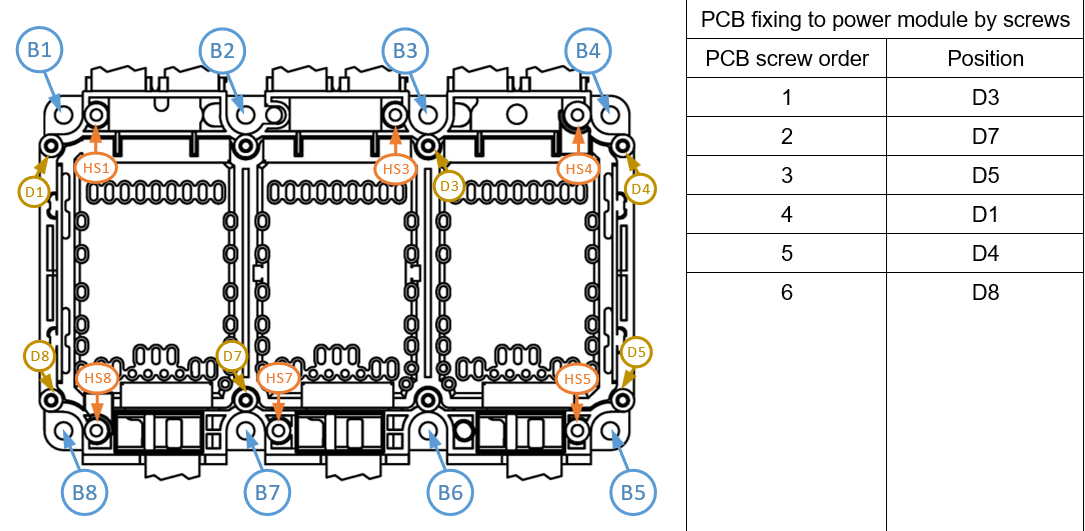
Screw order and module clamping during baseplate screw process
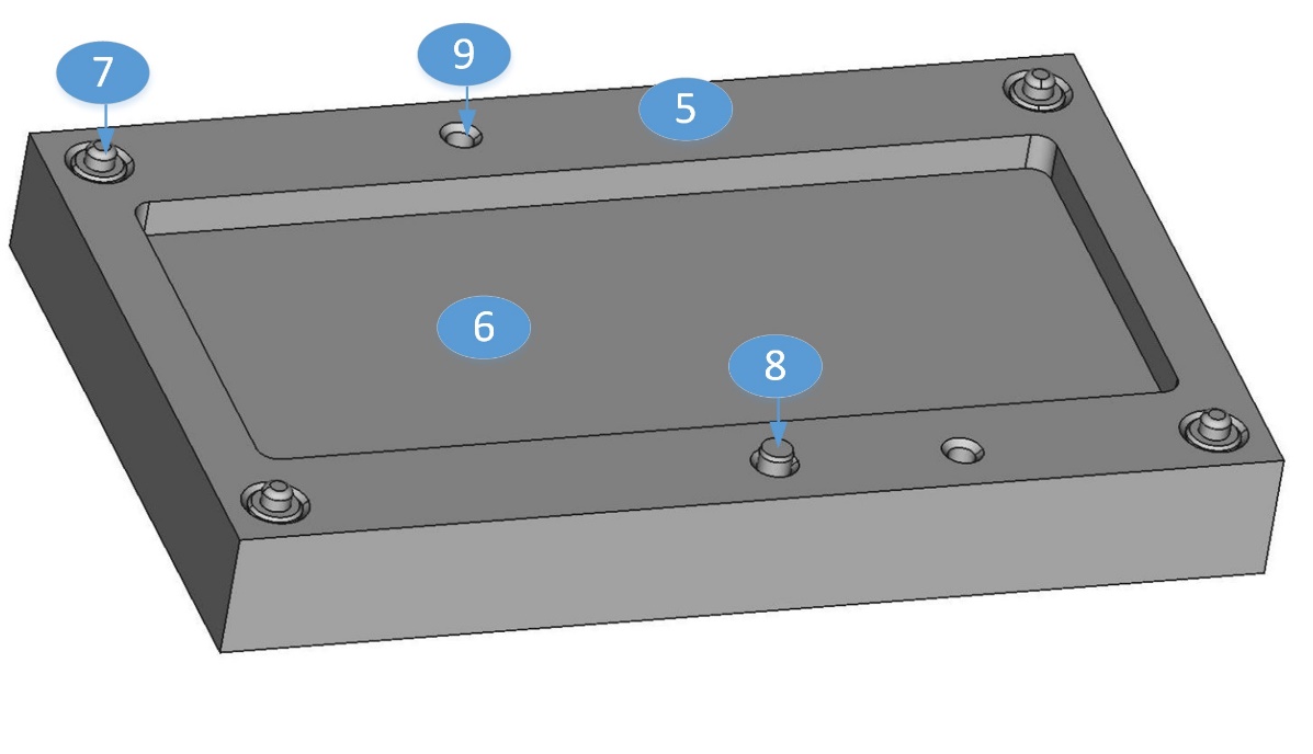
A correct screw order is required to avoid damage on the part. The eight baseplate holes are labeled in
Figure 19
(or see product datasheet
2
). Tighten the screws crosswise from inside to outside. The start position B2 is one possible example. The crosswise inside to outside mandatory method can also be modified to B3, B7, B6 as the start position.
Figure 19. Positions of baseplate screws (Bx) with correct screw order list
It is required to properly fix the power module to the cooler during the screwing process to avoid tilting of the module with possible damage (i.e., plastic deformation of the baseplate).
The following methods are preferred for module fixation during the screw process:
Multi-step screw mounting (only possible with metric screws): Place first and second screws, and fix with the lowest torque (this avoids only module tilting and will not provide a high clamping force). Fix third to eighth screws with a low torque (e.g., 0.4 Nm to 0.6 Nm). The clamping force of the third to eighth screws will ensure that the sealing ring is already finally compressed. Fix all screws with the final torque as specified
Module clamping (all recommended screw types): After the power module (with PCB) is placed onto the cooling system, the module should be clamped in the Z axis of the module with a total force of Fc = 2 kN to ensure that the sealing ring is fully compressed during the screwing process. The clamping can be performed by hollow cylinders (outer diameter 6 mm; inner diameter 3.6 mm) in the area of the heat stake domes (HS1, HS3, HS4, HS5, HS7, HS8. See Figure 19 ). The clamping force will be introduced in the seating location of the heat stake domes. If the screw domes (D1, D3, D4, D5, D7, D8) are used for clamping, it is important that the PCB is not further pushed down during the clamping process
PCB mounting on the module housing
The HybridPACK™ Drive G2 power module has implemented two options for fixing the PCB on the power module. The primary option is fixing via the heat stake domes, which brings the advantage of minimum inverter BOM. The second option is via self-tapping screws, which is a process known from the established first generation of HybridPACK™ Drive power modules.
Note that fixing the PCB to the module (either by heat stake process or by screws) is recommended only after the power module is attached and fixed to the cooling system.
PCB mounting by heat stake process
The heat stake method for fixing PCBs to the plastic frame can enable the lowest system BOM cost. For general information about the heat stake method, see
[8]
. The heat stake process can be easily adjusted to project-specific needs by different thermode geometries, heating/cooling profiles, and different force profiles. Table 7 specifies the maximum allowed boundary conditions of the power module during the heat stake process. This section describes the heat stake process within the specification of
Table 7
which was selected for evaluation tests.
No. | Description | Unit | Min. | Typ. | Max. | Notes/conditions |
|---|---|---|---|---|---|---|
1 | Maximum force on heat stake dome at start of the process | kN | – | – | 0.5 | This force is allowed onto the undeformed dome at the beginning of the heat stake process |
2 | Maximum force on heat stake dome at end of the process | kN | – | – | 1.8 | This force is allowed at the end of the process where the dome was already deformed |
3 | Simultaneous heat stake process on all 6 domes | – | – | Allowed | – | – |
4 | Maximum temperature during heat stake process | °C | – | – | 280 | Limited to a maximum of 10 s |
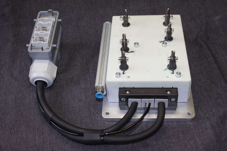
Example heat stake process
This section describes an exemplary heat stake process, which was developed by Hartmann Feinwerkbau GmbH
9
together with Infineon Technologies AG for evaluation and reference purpose. The example shows the process on one single dome, but simultaneous processing all six domes is also possible (see
Figure 23
).
Figure 20. Power module dome before (a) and after (b) the heat stake process
Figure 21. Example thermode design and setup of the evaluation tests 9
Figure 22. Example heat stake process. See the short description in Table 8
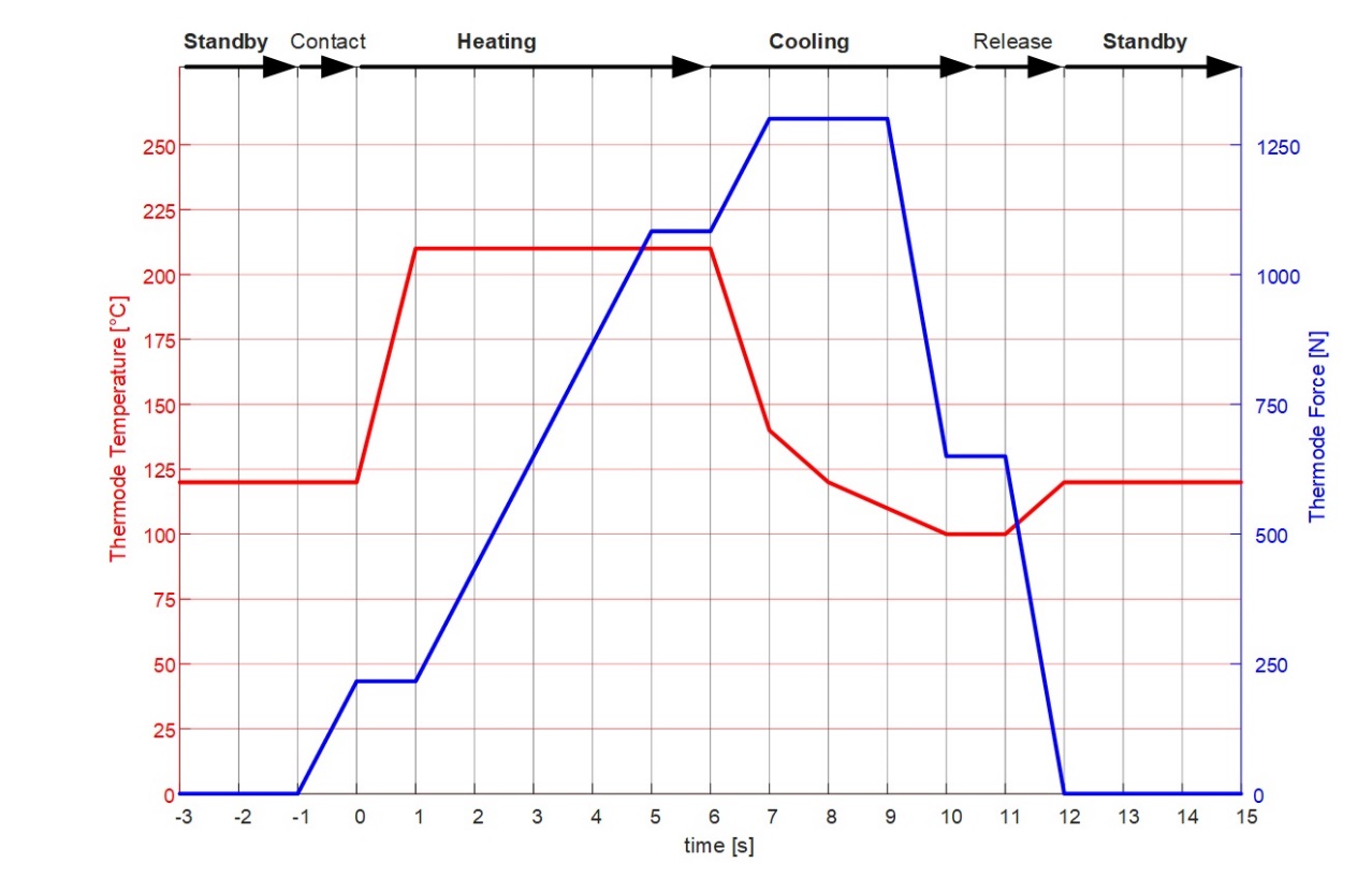
Phase | Description |
|---|---|
Standby | The equipment is in standby and ready for the process |
Contact | The thermode is located on the power module heat stake dome. A low contact force can be applied |
Heating | The thermode is heated up and the force increases together with the temperature to deform the plastic dome. The force can be applied by a hydraulic or compressed air system |
Cooling | At the beginning of the cooling phase, the force is further increased to the final end value. The dome is already deformed during the cooling phase. In the second phase of cooling, the force is quite rapidly ramped down to prepare the next release phase |
Release | The force is released. At the same time, the thermode can be already controlled to the standby temperature |
Standby | The tool is ready for the next heat stake process |
Figure 23. Tooling example for heat stake process of all six domes at the same time [8]
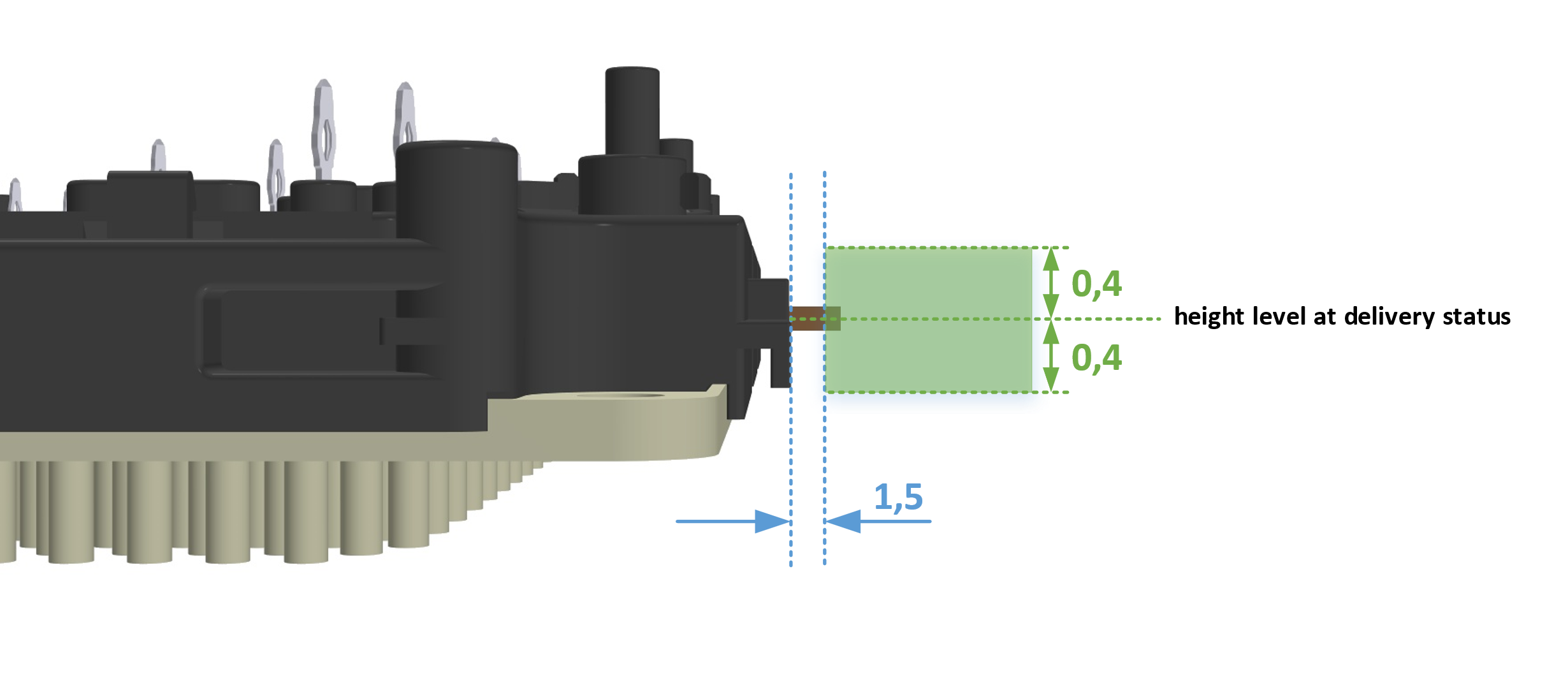
PCB mounting by self-tapping screws
PCB mounting by screws is an alternative method to the heat stake method. Select one mounting option. PCB fixing by both (heat stake and screws) was not tested and therefore is not recommended. The power module PCB screw domes were designed for the following screw type and process.
No. | Description | Unit | Min. | Typ. | Max. | Notes/conditions |
|---|---|---|---|---|---|---|
1 | Self-tapping screw type | – | – | EJOT Delta PT WN5451 30x10 | – | Recommended screw Screw tests at Infineon were performed with Zn5 plated screws |
2 | Mounting torque Meff (see product datasheet 2 ) Meff + Mw (for 1.6 mm PCB) | Nm | 0.45 1.1 | 0.50 1.2 | 0.55 1.3 | Mw ≈ 0.7 Nm torque is required for self-tapping of the 10 mm screw length, 1.6 mm PCB thickness, and 500 rpm mounting speed. This self-tapping torque is not effective for the mounting force and varies with the PCB thickness and effective screw length |
3 | Recommended mounting speed | rpm | 400 | 500 | 800 | Lower than 400 rpm is not recommended and can lead to dome crack or damage on the screw The maximum rpm mainly depends on the applied screw equipment |
4 | Screw order | – | – | Crosswise from inside to outside | – | For preferred order, see Figure 25 |
The initial 1.5 mm (approximately) of the mounting stand-off serves as guidance and cannot take any force. The thread in the plastics will form itself by driving in the EJOT screws. It is important to have an appropriate minimum turn-in speed, which causes a self-heating of the screw to have a proper thread forming in the plastic housing without splitting and cracking. Within the screwing process, there are no pauses recommended, like screw tightening in several steps (see also the smooth torque waveform over the time in
Figure 24
). An electronically speed-controlled screwdriver is the preferred aid for this purpose. Furthermore, a straight insertion of the screw into the stand-off must be observed during assembly.
Figure 24. EJOT Delta PT screw (a), measured screw torque until failure (b)
Figure 25. Positions of PCB screws (Dx) with correct screw order
Connecting to the power tabs (terminals)
The copper power tabs are tin-plated and are well suited for screw-type connections and welding processes. The allowed forces/movement of the power tabs (see
Forces on power tabs and allowed bending area
) during assembly must be considered for screw and welding processes.
In general, the power tabs can be connected from the top side and bottom side to the counterparts, like the DC-Link capacitor. There is also no restriction if three or more busbars are connected in the stack together. To have the best system compatibility between HybridPACK™ Drive G2 power modules with A7 and A8 and the Drive Generation 1 power modules with A6 (1.0 mm or 1.5 mm thick power tabs), it is recommended to have a connection from top side. The power tab top side has always the same location to the housing independent of the product variant.
Power tab connecting by screws
Several mounting options and screws or nuts are suitable like the following examples:
screw – power tab – busbar – nut
nut – power tab – busbar – screw
screw – busbar - power tab – busbar – nut
describes only the interface screw/nut to the power tab. The interfaces from busbar to screw/nuts must be evaluated.
Table 10
provides only a rough overview on the screw types. Different types may be possible with the same mounting torque if the base of the head or the spot face are comparable to the given types and the busbar material is suitable for such mounting.
Option | Screw/nut type | Mounting torque | Notes/conditions | |||
|---|---|---|---|---|---|---|
Unit | Min. | Typ. | Max. | |||
1 | M5 ISO 7380-2-A2-(TX) screw | Nm | 3.6 | 4.0 | 4.4 | – |
2 | M5 ISO 6923 nut | Nm | 3.6 | 4.0 | 4.4 | – |
3 | M5 ISO 4762 screw (M5 ISO 7090 washer) | Nm | 3.6 | 4.0 | 4.4 | Only considered for low-volume production and lab testing |
4 | M5 ISO 4032 nut | Nm | 3.6 | 4.0 | 4.4 | |
5 | M4 ISO 7380-2-A2-(TX) screw | Nm | 1.8 | 2.0 | 2.2 | For continuous terminal currents >500 Arms recommended are M5 screw options |
6 | M4 ISO 6923 nut | Nm | 1.8 | 2.0 | 2.2 | |
Power tab connecting by welding
The different variants of HybridPACK™ Drive G2 power modules have the same power tab material but variants with the following ending in the type designation have no screw holes and are well suited for welding the power tabs:
FSxxxRxxA7PxYYY or FSxxxxRxxA8PxYYY or FSxxMRxxA8MAxYYY (YYY => Power tab variant)
YYY= ___ (no ending) : Short tabs DC and AC without holes
YYY= LBC : Short DC tabs without holes, long AC tabs with holes
shows an example of power module without hole. These plain power tabs can be connected by means of welding processes. Evaluate the welding process with its specific parameters. A general recommendation to the process type or parameters is not possible as it is also depending on the companion material of the busbar and the available welding equipment. Studies of institutes give a comprehensive guide for the pre-selection of applicable welding process types. For example, see
7
,
8
.
Material property of the power tabs for selecting the welding process:
Copper type: Oxygen free copper type
Plating: Galvanic tin
Note that the power module frame must be limited to 185°C during the welding process.
A laser welding equipment supplier, which has already successfully performed pre-tests on HybridPACK™ Drive power tabs is listed in
8
. A weld line result is shown in
Figure 26
b.
Figure 26. HybridPACK™ Drive power module without holes at DC tab side suitable for welding (a). A weld line result on the power tabs (b)
Forces on power tabs and allowed bending area
During assembly, forces will be applied on the power tabs due to position tolerances of power tabs and the counterpart, like capacitor busbars. As forces cannot be directly measured during assembly, it can be hardly used as criteria for system design validation. HybridPACK™ Drive G2 modules have an allowed bending room of the power tabs (see
Figure 27
).
Note that the bending room must be a single event during assembly. The room can be applied simultaneously to all power tabs. A cyclic bending within the room during the application lifetime is not allowed.
Figure 27. Allowed bending room of the power tabs. Principal view can be applied to all power tabs of the module
System assembly clearance and creepage distances
The datasheet
2
of the HybridPACK™ Drive power module specifies the clearance and creepage distances of the product. It is known that external parts can modify these distances in the system. Therefore, it is mandatory to check the clearance and creepage distances of the entire final system assembly.
Check the distance between the cooler and housing (all external parts). This can be done only at the system level. Appropriate keepout or covering with isolating parts (plastic) can typically increase critical distances in the system design.
For systems with high DC working voltages, it is recommended to use the mounting method according to
Figure 4
a, where the alignment domes are within the assembly tools. The alignment domes will be removed after the assembly steps and will not limit the final clearance creepage distances of the product.
The mounting method according to
Figure 4
b, where the alignment dome is within the cooler housing, can reduce the creepage distances to 8.8 mm within the system setup. This method can be used for lower DC working voltages and/or if the alignment dome is made with an isolating material.
Phase current sensor integration
The HybridPACK™ Drive G2 power module is prepared for the coreless phase current sensor powered by Infineon XENSIV™ TLE4973 differential Hall sensor. This sensor is implemented in Swoboda CSM510HP2S or CSM510HP2D sensor modules, which fit into the sensor pocket and power tab slot of the power module. The sensor modules are available at Swoboda Technologies
10
. A limited number of samples for the evaluation purpose can be ordered also at Infineon (see
Table 1
for order numbers).
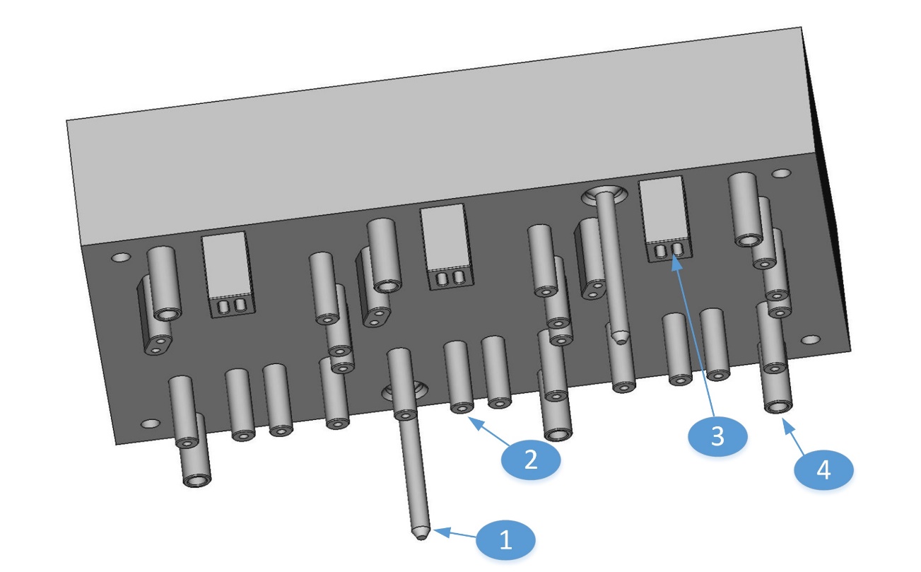
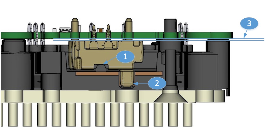
A vertical cross-section through the power module, sensor, and PCB is shown in
Table 1
. After the press-in processes, the sensor is located on the rotation-bar of the module (see 1 in
Figure 28
). The module sensor pocket and power tab slot is designed slightly wider than the Swoboda CSM510HP2S or CSM510HP2D sensor (see 2 in
Figure 28
). The remaining gap between the sensor and PCB (see 3 in
Figure 28
) was intended by design to compensate for mechanical tolerances.
Figure 28. Vertical cross-section of Swoboda CSM510HP2x sensor in HybridPACK™ Drive G2 power module
PCB footprint
The correct placement of the three sensors in the PCB design is shown in
Figure 29
. The PCB holes for the sensor and the power module can be designed with the same hole size and PCB specification. See
Table 2
for the PCB holes of the sensors. For more details of the PCB footprint, see
Figure 30
, which shows the sensor part in the same top view in
Figure 29
.
Figure 29. Sensor integration Swoboda CSM510HP2x. PCB footprint recommendation
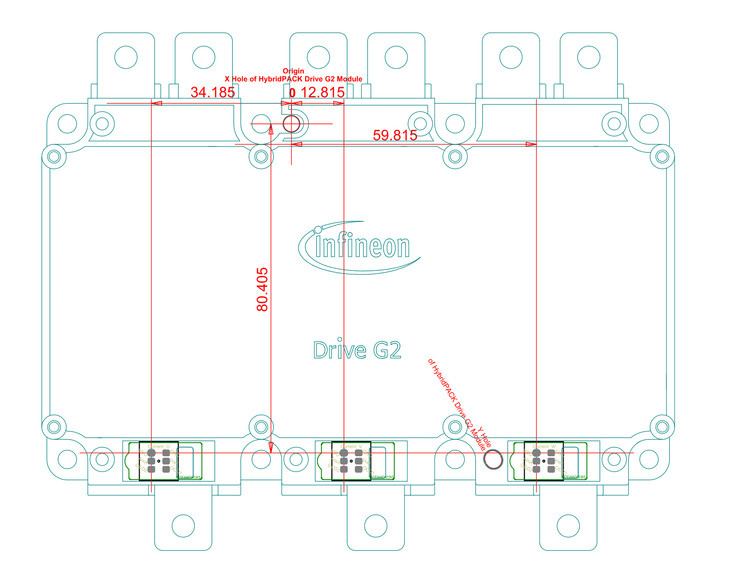
Figure 30. Sensor integration Swoboda CSM510HP2x. PCB footprint recommendation
Recommended non-plated guiding holes with 2.2 mm diameter
Press-fit holes; see Table 2
System design guidelines for magnetic parts close to the sensor
The phase current sensor detects a differential magnetic field above and below the AC power tab. This differential field is caused by the current flowing in the AC tabs. Any magnetic parts in the near field of the sensor can disturb the sensor signal. Therefore, do not place magnetic parts too close to the sensors in the system design.
Follow system design guidelines to avoid unintended signal disturbances.
Figure 31
indicates the different location areas for component placement and Table 11 lists the examples of allowed/restricted
2
parts in these areas.
Figure 31. Area categorization in the surrounding of the sensor module. The area is indicated with dimensions in X-Y but the same dimensions can be applied to the Z direction (center is the AC tab). Allowed/restricted parts in the individual areas are noted in Table 11
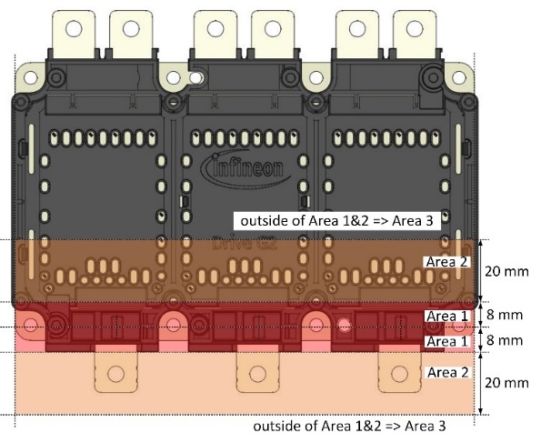
Area | Allowed parts examples 2 | Restricted parts examples 2 |
|---|---|---|
1 | All non-magnetic parts (plastics, aluminum, copper, etc.) PCB with Cu traces Standard components on PCB like ceramic capacitors, resistors, ICs (opamps, LDOs, etc.) Baseplate fixing screws according to Baseplate mounting on the cooler PCB fixing to the module according to PCB mounting on the module housing | Any type of shields or other ferromagnetic parts like Ni-plated busbars Transformers and chokes with larger than 10 mm edge length Avoid other screw types that are not recommended in this application note |
2 | All non-magnetic parts (plastics, aluminum, copper, etc.) PCBs with Cu traces Standard components on the PCB including SMD chokes and transformers Baseplate fixing screws according to section Baseplate mounting on the cooler PCB fixing to the module according to section PCB mounting on the module housing Power tab screws/nuts according to Connecting to the power tabs (terminals) or weld lines | Avoid any type of shields or other ferromagnetic parts with the exception: Cu busbars with Ni plating can be typically connected to the AC tabs in area 2 Avoid other screw types that are not recommended in this application note |
3 | All | None |
Assembly process of the phase current sensor
The phase current sensor modules can be assembled by two different concepts:
The assembly concept via self-alignment on the power module rotation bar allows to place the sensors first into the power module and subsequent the gate driver board is aligned and pressed onto the power module. This concept is described in Sensor assembly via self-alignment on power module rotation bar
For the alternative concept via two-step press-in process, the sensors must be pre-pressed into the gate driver board with an appropriate gap. In a subsequent step, the gate driver board with pre-assembled sensors will be aligned and pressed onto the power module. The concept is described in Sensor assembly via two-step press-in process
Independent of the applied assembly process, there is no need to adjust heights or tools when HybridPACK™ Drive G2 A7 or A8 with different AC tab thicknesses are used for a wide range of inverter platforms. The rotation bar in the module is designed in such a way that the co-developed differential Hall sensor is always positioned in the correct Z height. One sensor will fit to the entire HybridPACK™ Drive G2 platform, independent of the product derivate (A7 vs. A8, voltage classes, current levels).
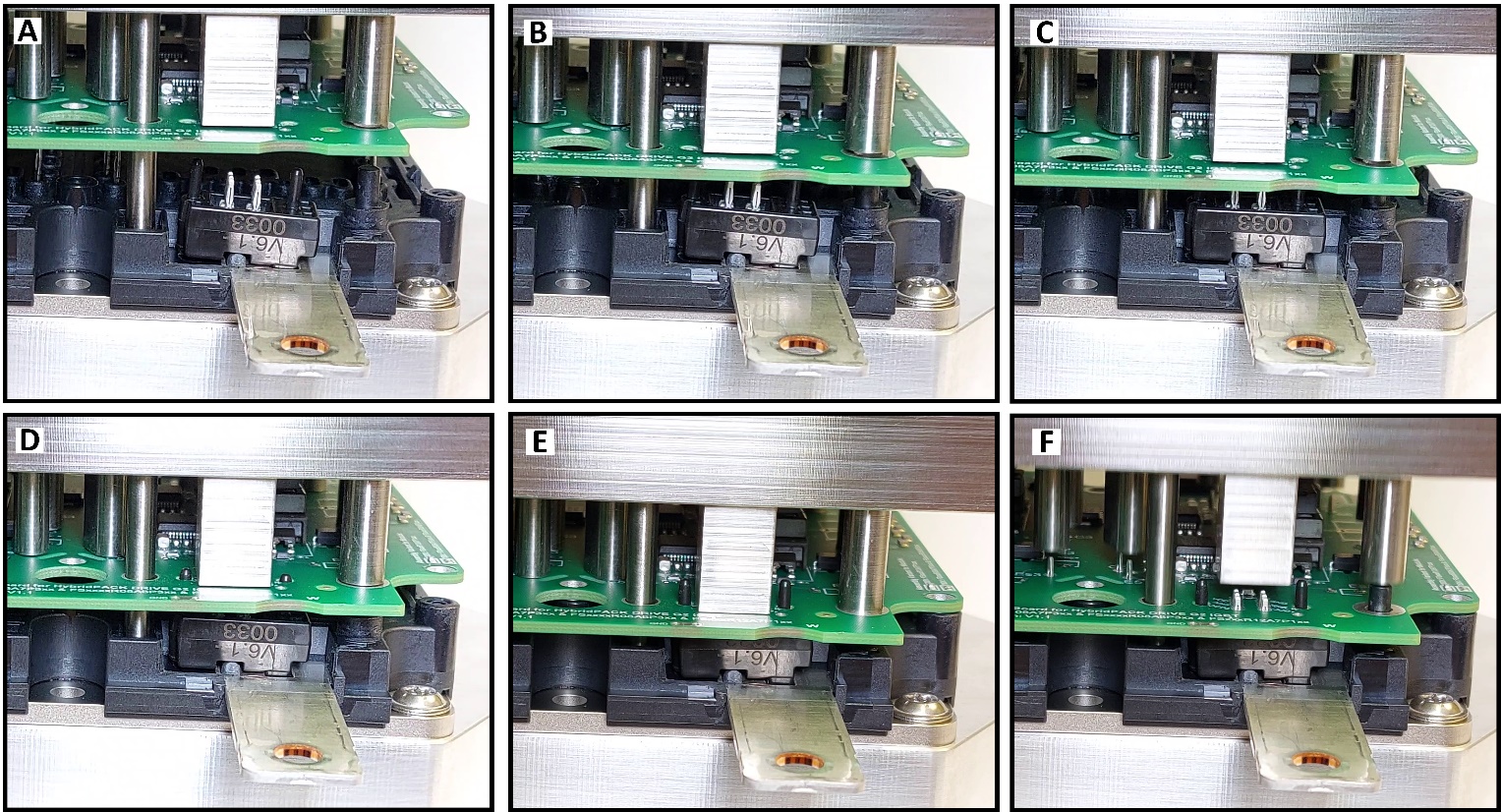
Sensor assembly via self-alignment on power module rotation bar
Place the three sensors directly into the power module sensor pockets. The shape of the power module sensor pocket and the shape of the sensor modules prevent incorrect assembly orientation (i.e., poka-yoke).
Figure 32
demonstrates a self-alignment feature. Note that
Figure 32
uses a special modified power module with a cut-out of the sensor pocket to make the sensor visible in this example. The sensor module was also specially prepared for an overscaled sensor tilt angle. This demonstrates the self-alignment feature in a scenario that exceeds worst-case tolerances.
A: It is normal for the sensor modules to be slightly tilted after they are placed into power module sensor pockets. For illustration purpose, an overscaled extreme tilted example is shown in Figure 32
B: It is normal for the sensor modules to be slightly tilted after they are placed into the power module sensor pockets. For illustration purpose, an overscaled extreme tilted example is shown in Figure 32
C: The alignment dome of the sensor module slides on the PCB. At the same time, the sensor rotates on the power module rotation bar and the sensor alignment domes automatically align with the PCB holes as shown in Figure 32
D: The PCB is self-aligned and all signal pins of the power modules and the sensors are located in the PCB holes. The press-tool further moves in the Z direction and applies press-in forces to the part as shown in Figure 32
E: The press-in process is the stop criteria, where the PCB is in its final position located on the heat stake/screw domes as shown in Figure 32
F: The press-tool is released. The PCB and sensors are in the final position as shown in Figure 32
Figure 32. Sensor assembly option uses self-alignment on the power module rotation bar. Note that the picture shows an overscaled extreme example for illustration purposes only
Sensor assembly via two-step press-in process
In this assembly concept, sensor modules are first positioned to the gate driver board and partially pressed-in with a certain distance. The final press-in process is the second step.
Pre-press-in process
illustrates the pre-press-in process.
An example of a sensor pre-press-in bottom tool
Positioning of the sensor modules on to the bottom tool
The gate driver board is aligned by guiding domes in the bottom tool
The gate driver board is already positioned on the sensors and all 18 sensor signal pins are in the PCB holes. The system is now ready for the pre-press-in process
The top tool is aligned and the press-equipment performs a press-in with a controlled way force method. The tools should have distance keepers to stop the press-process in such a way that about 1 mm gap between sensor and PCB is ensured
The status of the pre-pressed sensors in the PCB. The press-fit pins and sensors are not yet in the final position but the system has enough retention force for further handling (limited transport) purpose
The two-step press-in process described above shows the pre-mounting of three-phase current sensors simultaneously. It is also possible to use a pre-press concept by smaller tools, where only one sensor is pressed-in at a certain distance (e.g., by robot or manual with handling tools).
Figure 33. Sensor to PCB pre-press-in process
Final press-in process
illustrates the final press-in process.
The gate driver board with the pre-assembled sensors are aligned with the power module. See Module alignment and x,y guiding holes for detailed information about PCB to module alignment
The gate driver board including the sensors are pressed onto the module. See Press-tools and Press-in process for details. The sensors will position automatically to their correct final position during this process. A press-in curve with the three-phase current sensors is included and is shown in Figure 12
Figure 34. PCB with pre-assembled sensors pressed onto the module. The sensors will position automatically into their final correct positions due to the power module rotation bar
Sensor parameters
This section is not intended as a product specification of the TLE4973 sensor chip and/or the Swoboda sensor module.
Table 12
provides a short overview about typical settings in the use case of the HybridPACK™ Drive G2 power module.
Typical current rail transfer factor to the Hall sensor: 12.5 μT/A
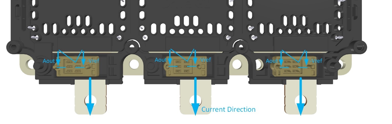
Figure 35. A positive current in this direction leads to a positive output voltage swing at the Aout pin and in case of full differential mode at the same time to negative output voltage swing at the Vref pin
Measurement range (Full scale) | Sensitivity range (Programmable) | Sensitivity (S) | Gain 1/S Fulldiff (semidiff) mode | Overcurrent detection (OCD) threshold setting (Setting: Current threshold) |
|---|---|---|---|---|
± 567 A | S6 (Code 24) | 3.17 mV/A | 158 (315) A/V | 6: ±678 A 10: ±901 A 14: ±1125 A 18: ±1348 A 22: ±1571 A 26: ±1795 A 30: ±2018 A 34: ±2241 A 38: ±2465 A 42: ±2688 A 60: ±3693 A |
± 756 A | S5.5 (Code 18) | 2.38 mV/A | 210 (420) A/V | |
± 850 A | S5 (Code 16) | 2.12 mV/A | 236 (472) A/V | |
± 972 A | S4.5 (Code 14) | 1.85 mV/A | 270 (541) A/V | |
± 1134 A | S4 (Code 12) | 1.59 mV/A | 314 (629) A/V | |
± 1361 A | S3.5 (Code 10) | 1.32 mV/A | 379 (758) A/V | 6: ±1695 A 9: ±2114 A 11: ±2393 A (default) 12: ±2532 A 30: ±5045 A 57: ±8814 A |
± 1701 A | S3 (Code 8) Default setting | 1.06 mV/A | 472 (943) A/V | |
± 2268 A | S2 (Code 6) | 0.79 mV/A | 633 (1266) A/V |
Traceability, data matrix, and part markings
Traceability of materials, equipment, and processes is mandatory for key automotive components. Therefore, the HybridPACK™ Drive G2 power modules are produced at Infineon in a seamless traceability environment. Nevertheless, traceability must not be aborted after the modules are shipped to the customer and assembled into the inverters. To reap the full benefit of a traceability chain, the unique module number (module ID) should be linked to the inverter ID at the customer side.
shows the module labels and where to find the DMX code necessary for tracing the module ID.
Figure 36. Module labels (typical appearance). For a seamless traceability the DMX code, which is the module ID (or the alternative type designation + date code + serial number) should be recorded and linked to the inverter ID
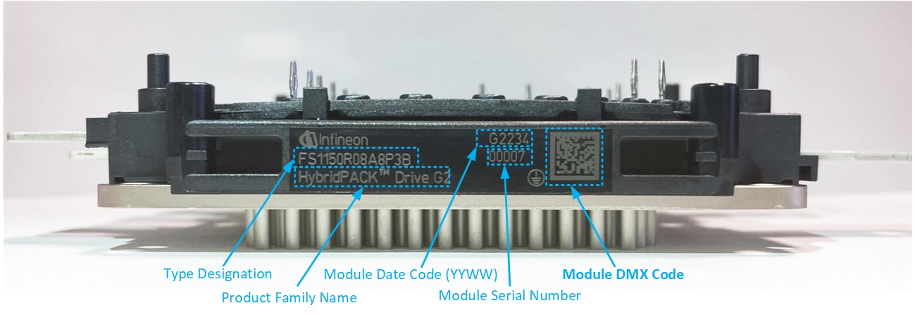
The content of the 23-digit code is as follows:
00007 | 049704 | 81592881 | 22 | 34 |
Serial No | Material No | Production order number | Date code Year | Week |
Engineers in the lab can also use free DMX code reader apps on their smartphones.
Android: QR Extreme, QR Droid, and many others supporting data matrix codes
iOS: i-nigma QR and many others supporting data matrix codes
Remark: Only productive parts without _ENG label have full traceability implemented. Prototypes and engineering samples (ES) can have different part markings; depending on development status none or just parts of the traceability measures are implemented.
Traceability of the shipping boxes (trays)
The
Figure 37
shows an example of the typical HybridPACK™ Drive shipping boxes, which is called "tray". A full tray contains six power modules. The power module gripper pockets are well accessible and should be used to pick the modules out of the boxes. The tray label codes are shown in
Figure 38
and the most relevant codes which can be used for traceability are explained in this section.
Figure 37. Power module trays (shipping boxes). The full tray contains six HybridPACK™ Drive G2 power modules
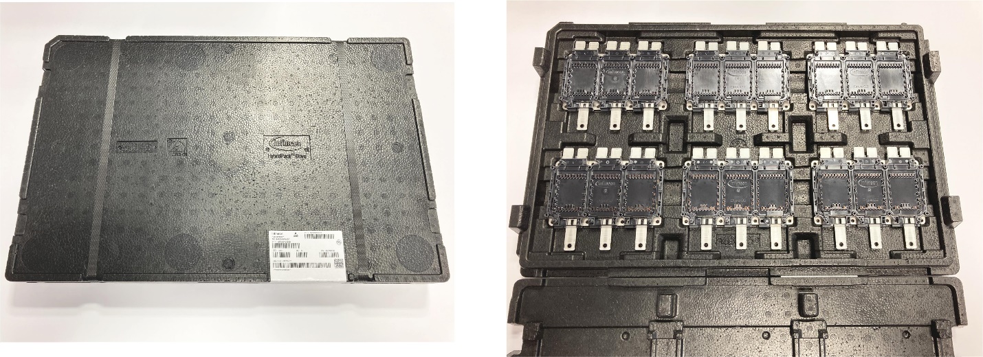
Figure 38. Tray label
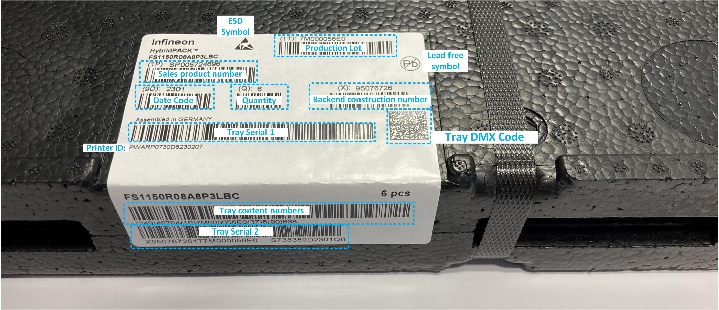
Date code: This has the format YYWW (YY = year, WW = production week)
Tray Serial 2: This number is the preferred option for traceability measures because it is also readable if trays are stored in a stack. The number is a composition of the back-end construction number, production lot, tray serial number, date code, and quantity. In this example, it contains the following data: X95076726 1T7M000056E0 S738389 D2301 Q6
Tray Serial 1: This number can be used for implementation of traceability measures. However, this bar code may not sometimes be readable if several trays are stored in a stack. The number is a composition of the back-end construction number, production lot, and tray serial number. In this example, it contains the following data:
X950767261T7M000056E0 S73838
Tray DMX code: This number can be used for implementation of traceability measures. However, it is not readable when trays are stored in a stack. The DMX code on the tray is a composition of all numbers stored in the other bar codes. In this example, it contains the following data (not relevant data is indicated with "#"):
∆## X95076726 1T7M000056E0 9D2301 Q6 1PSP005724696 ### ### ####FS1150R08P3LBC##### S73838∆ Back end construction number - production lot – date code - quantity - sales product number – product name (type designation) - tray serial number
Traceability of CSM510HP2x phase current sensor modules
The phase current sensor modules from Swoboda Technologies
10
have a 14 x 14 DMX code printed on the package. This code contains a 16-digit bijective number, which can be used for traceability of the package. The sensor has the TLE4973 chip implemented, which has a bijective chip ID number stored and is readable through the DCDI protocol from the microcontroller. See the
product datasheet
of the TLE4973 device for more information.
Figure 39. Tray label
Pin position and pin gauge
The HybridPACK™ Drive G2 power modules specifies the signal pin positions by gauge test (see corresponding product datasheets
2
). The gauge test ensures that pin positions and heat stake dome positions in the power module delivery state mate with customer PCBs.
The hole pattern specification of the pin gauge is shown in
Figure 40
. The signal pin pattern is adjusted to IGBT or SiC MOSFET power modules but the principle hole pattern specification from the drawing will remain the same. The real production equipment might have a different appearance but the hole pattern and test method remain the same as shown in
Figure 40
. The two 4 mm holes defining the coordinate system is only a marker of the power module coordinate system. The gauge is aligned by the heat stake domes to the power module. The parts are tested at the Infineon power module production line whether pin gauge can be applied to the module. A low force in module Z direction on the gauge is allowed (typical up to 10..20 N, which is uncritical for the module and its pins). When the pin gauge can be smoothly attached to the module, the test is rated as PASS.
The basic description of the test and pin gauge specification is placed only for information on how these modules are tested at Infineon production lines. It is not required at the customer side to test power modules at incoming inspection again.
Figure 40. Hole pattern specification of pin gauge. Hole pattern can be adjusted for another signal pinning (e.g., IGBT module vs. SiC MOSFET module) with the same hole size specification

Storage, transport, and handling
During transport and storage of the modules, avoid extreme forces through shock or vibration and extreme environmental influences. Storage of the modules at the limits of the temperature specified in the datasheet is possible, but not recommended. The recommended storage conditions are described in
1
.
Pre-drying of the power module prior to the press-in process (as is recommended for molded discrete components, such as microcontrollers, TO-cases, etc. designed for solder processes) is not required for the HybridPACK™ Drive G2 power modules.
For power module handling, use the implemented gripper pockets (see
Figure 41
and product datasheet package outline drawings). These 3 mm deep pockets are implemented in a functionally uncritical area. If it happens at all, abrasion or scratches from handling in this gripper pocket area does not have an influence on the power module function. Gripper tools can be designed as tight-fit and do not need much clamping force for handling the modules. Clamping forces of <20 N on each pocket is regarded as a very safe value.
Figure 41. Gripper pockets for power module handling (a). Typical handling gripper design principle view (b)
Power module appearance
This section explains frequent questions about the typical power module appearance.
Power tab tin plating
The power tabs are made of copper with a partial tin plating. The plating avoids visual discoloration and oxidation of the copper between power module production and mounting processes. After assembly, the tin plating has no function; the contact resistance is the same as an unplated pure copper power tab. To provide the maximum possible compatibility to various connecting techniques like screw type connections, clinching, and welding, it is mandatory to make the plating as soft as possible. Due to the desired compatibility and the required softness, visible scratches and/or not completely overplated edges due to the stamping process are of logical consequence (i.e., partial plating); it does not influence the product performance or quality.
Figure 42. Copper power tabs, which have a very soft tin plating and provides maximum compatibility to different mounting processes
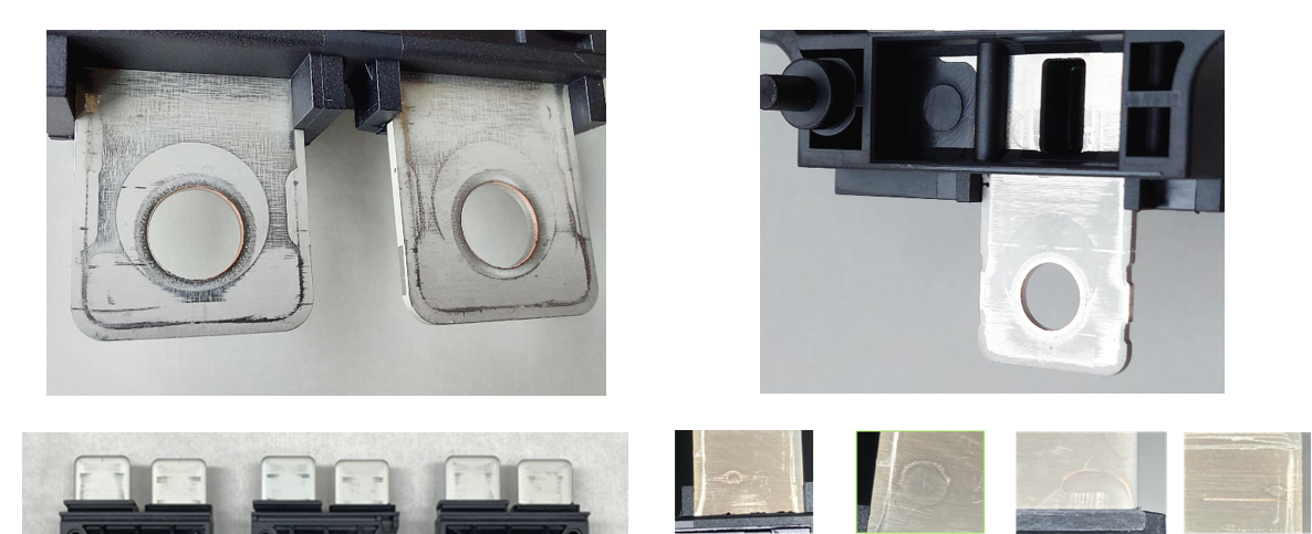
Baseplate surface
A typical appearance of the baseplate surface is called as "marbling" or "white spots" structure. This structure can be observed after the galvanic nickel and its cleaning process of the baseplates. The roughness of the baseplate, the chemical structure, and the thickness of the Ni layer is not different to baseplates, where this structure is not visible by the human eye. Such an appearance as shown in
Figure 43
is a normal appearance; it does not influence the product performance or quality.
Figure 43. Power module baseplate surface with a marbling or white spots structure
References
Infineon Technologies AG: Storage of products supplied by Infineon Technologies; Available online
Infineon Technologies AG: Product datasheet; Available online
HARTING Technology Group; Available online
Freudenberg Sealing Technologies; Available online
Infineon Technologies AG: PLASTIC COOLER HPD G1; Available online
Erwin Quarder Gruppe: HybridPACK Drive Kunststoff Kühler; Available online
Copper Development Association: Welding copper and copper alloys; Available online
Trumpf Laser- und Systemtechnik GmbH; Available online
Hartmann Feinwerkbau GmbH; Available online
Swoboda Technologies; Available online
Hitex GmbH: Reference cooler with sealing ring; Available online
Glossary
ESD
electrostatic discharge
ES
engineering samples
OAT
organic-acid-technology
OCD
overcurrent detection
PCB
printed circuit board
Revision history
Document revision | Date | Description of changes |
|---|---|---|
1.0 | 2024-02-20 | Initial release |
1.1 | 2025-02-26 | Template update; no content update |
1.2 | 2025-10-16 | Added Si/SiC Fusion tool |
1 The recommended press-tool uses the PCB area around the heat stake for press-stop. By design, plated holes with recommended annular rings ensure that the PCB thickness is the same at press-fit pins and press-stop areas.
2 The categorization of allowed and restricted parts in the areas is a non-binding recommendation based on best practice/experimental studies and must be validated in the individual system design.