AN-DC6i-ASSEMBLY Assembly instructions for the HybridPACK DC6i
About this document
Scope and purpose
This application note describes the recommended process for mounting the HybridPACK™ DC6i power module. To ensure a robust design meeting the high quality demands of the automotive industry, it is important to use the right mounting order and appropriate printed circuit board (PCB) material, screw types, and processes.
Intended audience
Engineers and operators involved in the assembly of the HybridPACK™ DC6i power module into power electronics systems.
General information
This application note provides mounting instructions for the HybridPACK™ DC6i module with recommendations how to screw the module, assemble the PCB, and mount the module onto the heatsink.
Ensure that the ground straps should be worn while working with the components and that the ESD safety instructions must be followed at all times, since IGBT modules are electronic-static sensitive components. In addition, this application note does not cover all types of applications or conditions. As a result, the application note cannot replace a detailed assessment and examination of the suitability of the targeted applications carried out by you or your technical divisions. In any event, the application note will not become part of any supplier-agreed warranty, unless the supply agreement determines otherwise in writing.
Recommended mounting order
All datasheet drawings specify the power module at the delivery point. When the power module is mounted to a cooling system, deformations can occur (that is, depending on the cooler flatness and screw torque). The following mounting order can be recommended:
Align PCB to the power module (the X-pins will support this process)
Press-in PCB (controlled way-force press-in process is recommended)
Prepare cooling system using the sealing ring
Attach the power module with PCB to the prepared cooling system
Fix the module baseplate on the cooler by screws
Fix the PCB on the power module by screws
Connect the module power tabs to busbar, capacitor, etc.
Press-fit assembly
Requirements for the PCB
The press-fit technology used in the HybridPACK™ DC6i is designed based on IEC 60352-5 for standard FR4 printed circuit boards with immersion tin plating. The PCB material must be compliant with IEC 60249-2-4 or IEC 60249-2-5 for double-sided printed circuit boards and IEC 60249-2-11 or IEC 60249-2-12 for multilayer printed circuit boards.
The PCB requirements are given in Table 1. If these requirements are not met, there is a risk of a not gas tight signal pin connection, or that the pin and/or the PCB may be damaged. The PCB recommendations for the X-pin holes are given in Table 2.
It should be noted that the press-fit hole specifications are valid only for assembled PCB. For unassembled PCBs, such as for testing purposes, a standard reflow solder process is recommended before the power module assembly process begins.
| No. | Description | Unit | Minimum | Typical | Maximum | Remarks and known common mistakes |
|---|---|---|---|---|---|---|
| 1 | Drill tool diameter | mm | 1.12 | 1.15 | Wrong drill tool used. Specify clearly the press-fit hole positions and required drill tool size to the PCB manufacturer | |
| 2 | Copper thickness in hole | μm | 25 | 50 | In case the via metallization is lower than the specification, the risk of a damaged/cracked via is high | |
| 3 | End hole diameter | mm | 1.02 | 1.10 | End-hole diameters lower than specification may lead to an increase in press-in forces (typically >115 N per pin,) which may damage the pins. Larger holes than specification may lead to low press-in forces (typically <40 N per pin) and can result in not gas tight connections | |
| 4 | Copper thickness of conductors | μm | 35 | 70 105 | 400 | No results are available for thinner or thicker copper layers |
| 5 | Hole-to-hole pattern tolerance | μm | ±100 | In a typical PCB manufacturing process, the hole-to-hole pattern is lower than ±80 μm | ||
| 6 | Recommended PCB thickness | mm | 1.6 | Target value with tolerance of ±10% thickness | ||
| 7 | Metallization of circuit board | Immersion tin (Sn chemically) | Immersion tin has type 1–5 μm metallization in the hole. Other metallization types should be avoided because they can lead to strong deviations in press-in forces. For example, HAL leadless materials show high variations in press-in forces and could result in a non-gas-tight connection, which can fail over the application lifetime. PCBs with ENIG plating can lead to increased press forces due to their hard surfaces; however, this PCB type was not tested in the Infineon module qualification tests | |||
| 8 | Metallization of pin | Ni/Sn (galvanic) | Sn-plated pin with nickel underlayer avoids potential whisker growth out of the upper galvanic tin layer | |||
| No. | Description | Unit | Minimum | Typical | Maximum | Remarks and known common mistakes |
|---|---|---|---|---|---|---|
| 1 | End hole diameter X-pin | mm | 5.9 | The hole should be drilled using a 6.0-mm drill tool and not milled to avoid unnecessary hole position tolerances | ||
| 2 | End hole diameter Y-pin1 | mm | 5.4 | The hole should be drilled using a 5.5-mm drill tool and not milled to avoid unnecessary tolerances of the hole position | ||
| 3 | Hole-to-hole pattern tolerance | μm | ±100 | Plated holes are preferred to achieve a minimum tolerance between the “X-pin hole” and “press-fit hole” pattern |
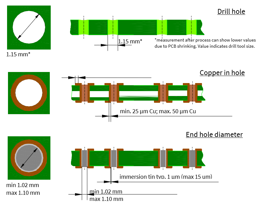
Figure 1 illustrates the structure of a PCB according to the specification in Table 1. The hole in the PCB is drilled using a 1.15-mm drill tool. It is normal for PCB material to shrink after drilling process. Therefore, a hole size of 1.15 mm should not be understood as a check gauge after drilling, but rather as an illustration for understanding the PCB stack.
Figure 1. Structure of a PCB according to the specification in Table 1
General hints for the PCB footprint
The footprint of PCBs usually depends on PCB manufacturing processes and customer-specific design rules. The best practices and starting point for system design are summarized in Table 3.
| No. | Type | PCB implementation hint |
|---|---|---|
| 1 | X-pin holes |
|
| 2 | Signal press-fit pin holes | See Table 1 |
| 3 | Components keep out of the press-fit pins |
Others:
|
| 4 | PCB fixing screw holes |
|
Press-in tools
This chapter describes a sample press-in tool, which can be adapted to project specific details such as PCB assembly locations, maximum height of other PCB parts, etc. to avoid mechanical collisions during the press-in process. The press-in tool is made of two parts (see Figure 2 and Figure 3).
Figure 2. Recommendation upper tool
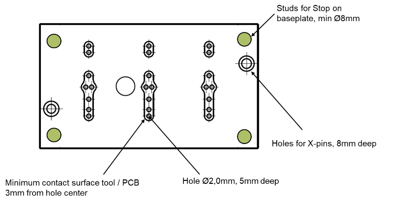
Figure 3. Recommendation lower tool
The lower tool supports the baseplate of the power module and must avoid damage to the pin-fin cooling area. In order to prevent scratches and damage to the baseplate sealing area, the material and/or plating of the bottom part of the tool must be selected. The holes for the X-pins prevent the wrong orientation of the power module in the press-tool by using the poka yoke concept.
The upper tool supports the PCB with cylindrical shapes around the press-fit pins during the press-in process. This part of the tool must be made of material capable of withstanding press-in forces. In order to avoid a press-in process with an incorrectly oriented tool or power module, the top tool also has cylindrical holes around the X-pins.
The following points must be taken into account when using the press tool:
Press-tool distance keeper (Studs) should be placed at the positions of the 4× module baseplate holes
Press-tool distance keeper (Studs) should have a minimum diameter of 8 mm
Maximum press-in force specified in Table 4
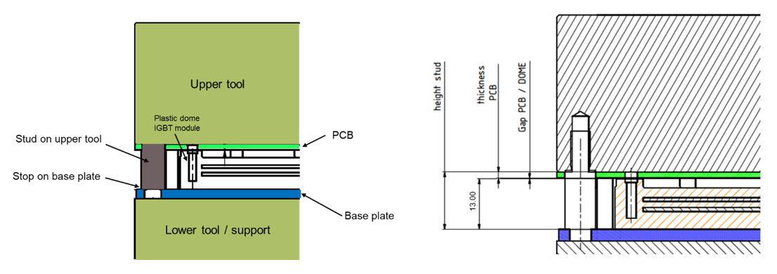
Press-tool distance keeper height: typically, the gap between the PCB and module housing domes should be 150 µm after the press-in process
The total hight of the distance keeper is 14,6 mm (typical dome height is 12,85 mm + 150 μm gap between the PCB and module domes + 1,6 mm)
Press-in process
For serial production, it is recommended to use a press-in process with a controlled force-distance.
Figure 4. Typical way-force press-in figure from a HybridPACK™ DC6i module with 21 signal pins
Figure 4 shows an example of a HybridPACK™ DC6i press-in process. When the force increases, the press-in process begins. The z-axis in this figure is set to 0 mm at this point. In case an initial high peak is detected, it may indicate a failure in the process, such as PCB hole plugged with solder, not properly inserted PCB before the process starts, machine collision with other external parts, etc.
The force curve increases smoothly when the PCB is pressed down (see Figure 4). Lower press-in speeds (see Table 4) are not allowed because the press-in forces may increase and damage the pin. High press-in speeds are not critical for the module.
A significant slope change can be detected at the end of the process considering the first derivative of the force-distance figure (see Figure 4). At this point, the PCB is fully pressed on the module housing and the effective part of the press-in process is completed.
At this point, the force should be at least 40 N per pin (that is, 840 N for HybridPACK™ DC6i with 21 pins).
It should be noted that the press-in equipment must be designed for the expected high forces. During the press-in process, the bottom and the top press tool must be parallel to each other and mechanically fixed without tilt.
| No. | Description | Unit | Minimum | Typical | Maximum | Remarks |
|---|---|---|---|---|---|---|
| 1 | Press-in speed | mm/s | 0.4 | 2–4 | 8 | During the press-in process, it is not allowed to exceed the minimum speed (no multistep press-in process). The maximum press-in speed is typically limited due to the non-ideal press machine |
| 2 | Maximum allowed press force | kN | 4 |
PCB design hint for high thermal cycle system robustness
In particular, in applications where high module ambient temperatures and/or high thermal cycle stress are expected, it is recommended that the system design be carefully designed to minimize pin-pull forces. The following parameters can be optimized in the system design:
PCB mounting positions (for example, see PCB design for module external mounting)
PCB design for module external mounting
Press-in tools describes the press-tool and the distance (gap) between the PCB and the dome.
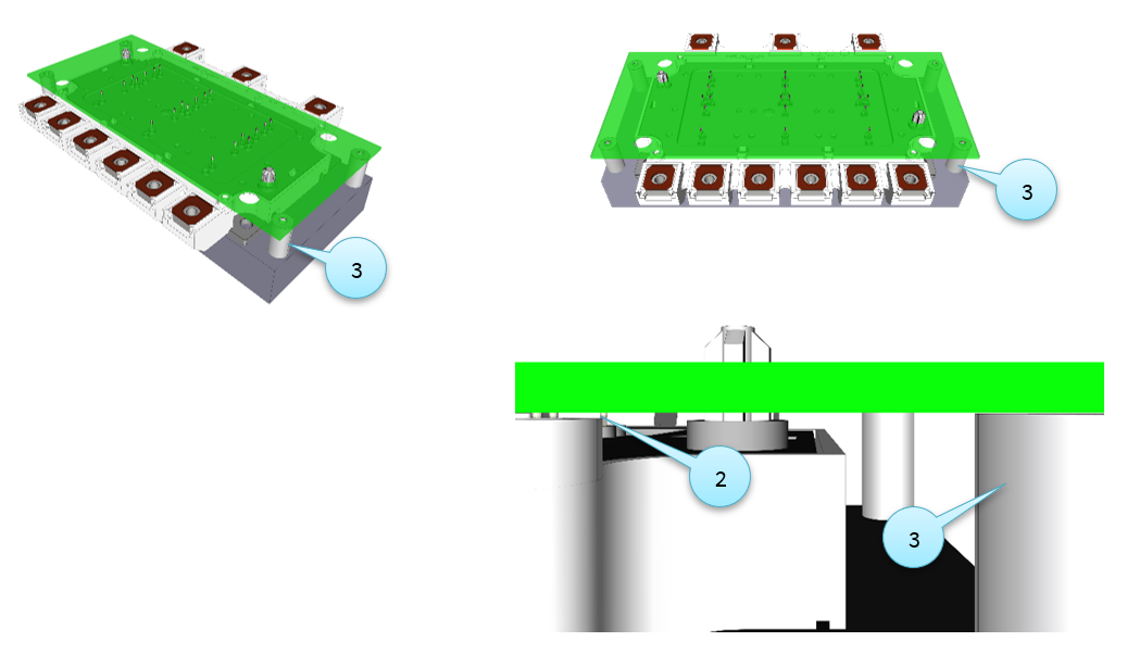
After press-in, a gap remains between the bottom side of the PCB and the housing domes of the power module (see area (2) in Figure 5). The inverter system designer can implement a PCB fixing point outside of the power module (see area (3) in Figure 5). The fixing point should be designed in such a way that a gap of 150 µm is achieved after pressing process (height of the fixing point is ~16 mm). After fixing the PCB with screws to the fixing point, no screws (that is, Ejot screws) are allowed at the module domes in the case of the external fixation method. There is a small gap between the module and PCB, which must remain after the final assembly.
Figure 5. Example module with externally mounted PCB. The distance keeper from the press tool ensures the distance between the PCB and the module dome (2). The PCB can be fixed externally of the module (3).
Power module cooling system
The cooler design has a significant impact on the overall cooling performance, which means the combination of thermal resistance/impedance, pressure drop, and cooling flow rate. For all of these thermal-related product specifications, a reference cooling system is therefore needed where the given specifications are valid.
Reference cooler design
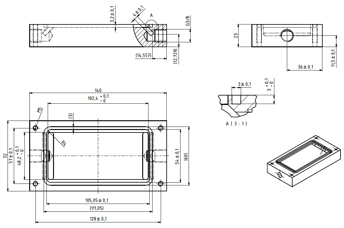
Figure 6. Reference cooler design for HybridPACK™ DC6i
Recommendation for the sealing ring
The power module baseplate is designed with a flat 7-mm region surrounding the entire wave area (see Figure 7).
Figure 7. Sealing region with 7 mm surrounding the wave area
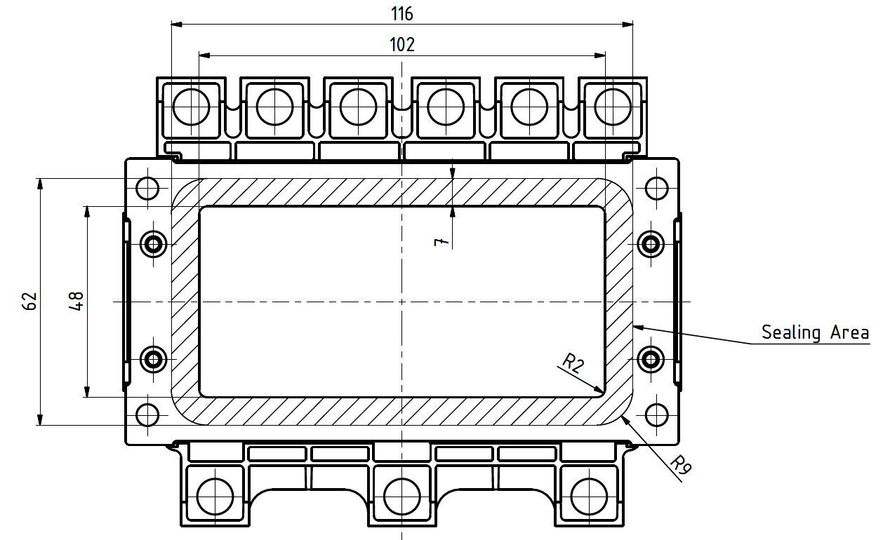
Figure 8. Drawing of sealing ring
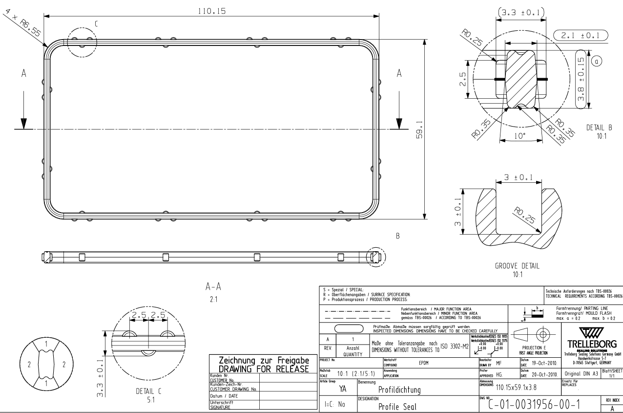
The HybridPACK™ DC6i module with a sealing ring from Trelleborg is recommended. Trelleborg designed a sealing ring with the article number: C-01-0031956-00-1.
Cooling fluid
It is not possible to provide a general recommendation for a specific cooling fluid as the power module is only one part of the entire cooling system. To find appropriate coolant fluid, the following items must be considered at the system supplier:
Coolant fluid with its corrosion protection must be compatible with the aluminum of the cooler material and with the nickel overplated copper baseplate of the module
Other parts of the coolant system must also be compatible with the fluid type (for example, Zn screws and chrome parts are generally not allowed in the cooling system)
The fluid mixture must have sufficient anti-freeze for the application conditions. Freezing of the fluid must be strictly avoided. Freezing fluid leads to plastic deformation of the baseplate of the power module and may lead to fluid leakage and/or isolation failure
Figure 9. Example of HybridPACK™ DC6i FS650R08A4P2 after long-term testing with G30™ fluid.
The aluminium cooling structure may appear black after the test. The organic corrosion protection reaction is a known effect and has no negative influence on the thermal performance or aging of modules.
Screw types and processes
Baseplate mounting screws
The clamping force of the module resulting from the assembly process to the heatsink depends on the torque applied and the heatsink material. The following torque values specified in the datasheet result from steel screws in aluminium heatsinks with a dry M5 thread.
The recommended screw order can be found in Screw orders (baseplate and PCB).
| No. | Description | Minimum | Typical | Maximum | Remarks |
|---|---|---|---|---|---|
| 1 | Mounting torque | 3 Nm | 6 Nm | ||
| 2 | Effective length of screw in cooler | 7 mm |
Fixation/clamping of the module during the baseplate screw process
To avoid tilting of the module with possible damage (that is, plastic deformation of the baseplate), it is necessary to properly fix the power module to the cooler during the screwing process.
The following methods are preferred for module fixation. Screw orders are listed in Screw orders (baseplate and PCB) as follows:
Multi-step screw mounting: Place screws 1 and 2 and fix with the lowest torque. This prevents only module tilting and does not provide a high clamping force. Fix screws 3 and 4 with low torque (for example, 0.4–0.6 Nm). Fix screws with the final torque as specified
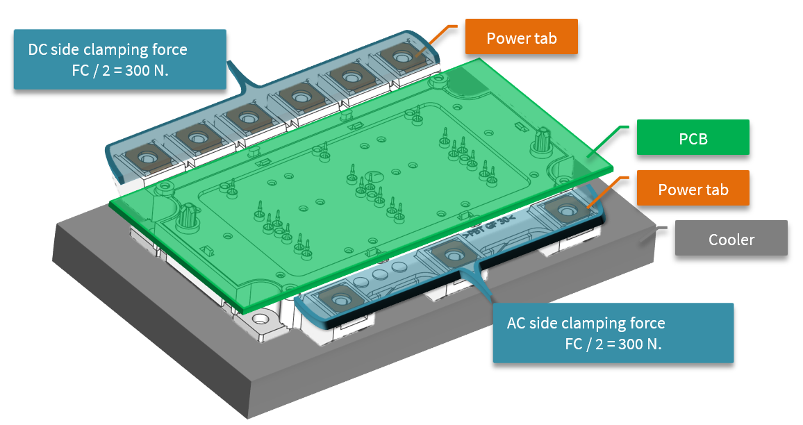
Module clamping: After placing the power module (with PCB) onto the cooling system, the module should be clamped along the z axis with a total force of Fc = 600 N (300 N per AC/DC side). Clamping can be performed in the area where the power tabs are located (see Figure 10). During clamping, it is important that the PCB or the pins are not further pushed down
Figure 10. Indicated area where the module can be normally clamped/hold down to the cooling system during the baseplate screw process
PCB mounting screws on the module housing
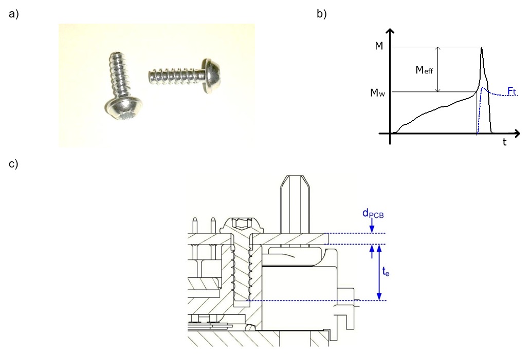
It should be noted that after the module is attached to the cooling system, it is recommended to attach the PCB to the module with screws. The module dome is designed for the following screw type:
EJOT Delta PT WN5451 30 × 10 (for 1.6 mm PCB thickness)
The thread in the plastics will form when the EJOT screws are driven. It is important to have an appropriate minimum turn-in speed, which causes self-heating of the screw, in order to form a proper thread in the plastic housing without splitting and cracking. For this purpose, an electronically speed controlled screwdriver is preferred. Furthermore, a straight insertion of the screw into the stand-off must be observed during assembly.
Figure 11. Typical appearance of the EJOT Delta PT (a), the basic mounting torque diagram (b), and a cross-section drawing of the PCB screw in the module dome (c)
| No. | Description | Unit | Minimum | Typical | Maximum | Remarks |
|---|---|---|---|---|---|---|
| 1 | Mounting torque Meff Meff + Mw (for 1.6 mm PCB) | Nm | 0.45 | 0.50 1.0 | 0.55 | Mw ≈ 0.45–0.5 Nm torque is required for the self-tapping of a 10-mm screw length and 1.6-mm PCB thickness. This torque is not effective for the mounting force Ft and may vary with screw length and PCB thickness |
| 2 | Recommended mounting speed | rpm | 400 | 600 | Lower than 200 rpm is not recommended | |
| 3 | Screw length in the module dome (te) | mm | 6 | 9 | Typical screw length of 10 mm for 1.6 mm thick PCBs |
Screw orders (baseplate and PCB)
The screw order shown in Figure 12 is crucial for avoiding damage to the part. Baseplate mounting screws and PCB mounting screws on the module housing specify the screw type and torque as well as the required processes, such as module fixation/clamping during the baseplate screw process.
Figure 12. Screw order for baseplate and PCB screws
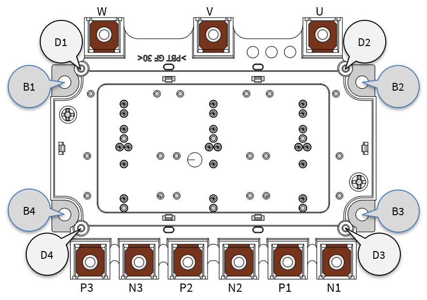
| Baseplate fixing after module assembly into cooler | PCB fixing after baseplate screwing | ||
|---|---|---|---|
| Baseplate screw order | Position | PCB screw order | Position |
| 1 | B1 | 1 | D1 |
| 2 | B3 | 2 | D3 |
| 3 | B2 | 3 | D2 |
| 4 | B4 | 4 | D4 |
Connecting to the power terminals
For the connection of power terminals, DIN M5 screws which comply at least with class 6.8 are required in combination with a suitable washer and spring washer or a complete combination screw.
When selecting the bolt length, the layer thickness of the connecting parts must be subtracted from the total length of the screws. The actual length of engagement into the module thread should not exceed the maximum specified depth of 10 mm.
As shown in Figure 13, the connected parts must be mounted to the power terminals in such a way that the specified static forces are not exceeded during assembly or later in operation.
Figure 13. Maximum permissible static pull-and-push forces at the power terminal
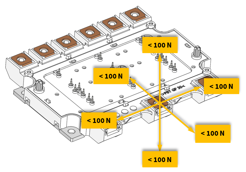
Table 8 show screws recommended for connecting the power terminals.
| No. | Description | Minimum | Typical | Maximum |
|---|---|---|---|---|
| 1 | Mounting torque | 3 Nm | 6 Nm |
Storage and transport
During transport and storage of modules, it is necessary to avoid extreme shocks or vibrations as well as extreme environmental influences.
It is possible to store modules at the temperature limits specified in the datasheet, but this is not recommended.
According to IEC60721-3-1, class 1K2, storage conditions should be ensured for a maximum storage time of 2 years.
Maximum air temperature: Tmaxair = +40°C
Minimum air temperature: Tminair = +5°C
Maximum relative humidity: 85%
Minimum relative humidity: 5%
Condensation: not permissible
Precipitation: not permitted
Icing: not permitted
The HybridPACK™ DC6i power modules do not require pre-drying of the power module prior to the press-in process (as is recommended for molded discrete components, such as microcontrollers, TO-cases, etc.
Traceability, data matrix, and part markings
The traceability of materials, equipment, and processes is essential for key automotive components. Therefore, HybridPACK™ DC6i is produced at Infineon in a seamless traceability environment. However, traceability must not be interrupted once the modules have been shipped to the customer and assembled in the inverters. In order to make full use of the traceability chain, a unique module number (module ID) must be linked to an inverter ID at the customer's side.
Figure 14 shows the module labels and where to locate the DMX-code necessary for tracing the module ID.
Figure 14. Typical module label appearance. In order to ensure seamless traceability, the DMX code, which is the module ID (or, alternatively, the type designation + date code + serial number), should be recorded and linked to the inverter ID.
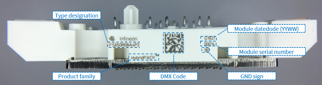
The DMX code can be read by all professional data matrix code scanners compatible with the IEC24720 and IEC16022 standard.
Engineers in the laboratory can also use free DMX code reader applications on smart phones:
Android: QR Extreme, QR Droid, and many other applications that support data matrix codes
iOS: i-nigma QR and many other applications that support data matrix codes
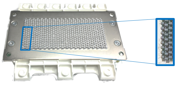
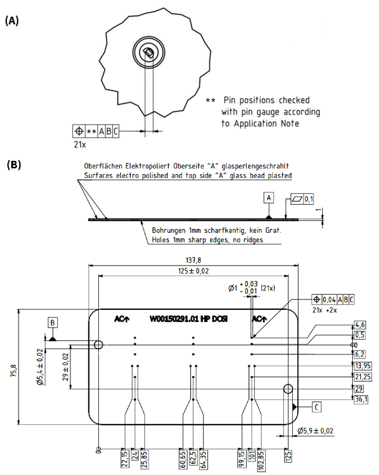
Pin position and pin gauge
A pin gauge test is implemented in the production line at Infineon for power modules that have a note in product specification, as shown in Figure 15A. Figure 15B shows the specifications of this pin gauge for pinning as implemented in FS650R08A4P2. In the production of the power module, the parts are tested to see if the pin gauge can be applied to the module. A low force in the z-direction of the module on the gauge (typically up to 10–20 N, which is uncritical for the module and its pins) is allowed. If the pin gauge can be easily attached to the module, the test is rated as PASS, which can be seen as a test if the customer is able to smoothly assemble the PCBs on the power module.
A basic description of the test and pin gauge specifications is provided only for information on how these modules are tested at Infineon production. At the customer side, it is not necessary to test the power modules again at the incoming inspection.
Figure 15. Extract of the datasheet regarding the pin positions for example FS650R08A4P2 (A). Infineon pin gauge specifications for the power module production test (B)
Power module appearance
This chapter explains frequently asked questions about typical power module appearance.
Pin rotation
The position tolerance is an important value and ensures that the PCB designed according to the recommendations fits the power module. The positions of the pins are clearly indicated in the product datasheet.
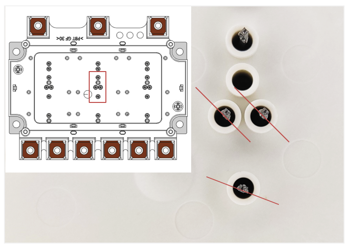
The pin rotation is not fixed because the interface (PCB via) is totally symmetric. The asymmetric pin geometry (that is, three contact press-fit pins) clearly indicates the pin rotation. Figure 16 shows an example, where the rotation is indicated: Typically about 45° pin rotations can be seen. However, there may be different angles in the final product, which does not give rise to objections and has no influence on the quality of the final contact.
Figure 16. Pins are not symmetrical (three contact press-fit pins) and a rotation angle is visible. Different angles may occur in the final product, but does not affect the contact quality and there is no reason for objection.
Revision history
| Document version | Date of release | Description of changes |
|---|---|---|
| 0.9 | 2019-09 |
|
| 0.95 | 2020-04 | Revised:
|
| 1.0 | 2020-09 | Added new chapters:
|
| 1.1 | 2023-12-07 |
|