XMC4500
XMC4000 Family
Microcontroller Series for Industrial Applications
ARM® Cortex®-M4
32-bit processor core
Datasheet
About this Document
This datasheet is addressed to embedded hardware and software developers. It provides the reader with detailed descriptions about the ordering designations, available features, electrical and physical characteristics of the XMC4500 series devices.
The document describes the characteristics of a superset of the XMC4500 series devices. For simplicity, the various device types are referred to by the collective term XMC4500 throughout this manual.
XMC4000 Family User Documentation
The set of user documentation includes:
- Reference Manual
describes the functionality of the superset of devices.
- Datasheets
list the complete ordering designations, available features and electrical characteristics of derivative devices.
- Errata Sheets
list deviations from the specifications given in the related Reference Manual or Datasheets. Errata Sheets are provided for the superset of devices.
Attention:
Please consult all parts
of the documentation set to attain consolidated knowledge about your device.
Application related guidance is provided by Users Guides and Application Notes .
Please refer to http://www.infineon.com/xmc4000 to get access to the latest versions of those documents.
Summary of Features
The XMC4500 devices are members of the XMC4000 Family of microcontrollers based on the ARM Cortex-M4 processor core. The XMC4000 is a family of high performance and energy efficient microcontrollers optimized for Industrial Connectivity, Industrial Control, Power Conversion, Sense & Control.
CPU Subsystem
CPU Core
High performance 32-bit ARM Cortex-M4 CPU
16-bit and 32-bit Thumb2 instruction set
DSP/MAC instructions
System timer (SysTick) for Operating System support
Floating Point Unit
Memory Protection Unit
Nested Vectored Interrupt Controller
Two General Purpose DMA with up-to 12 channels
Event Request Unit (ERU) for programmable processing of external and internal service requests
Flexible CRC Engine (FCE) for multiple bit error detection
On-Chip Memories
16 KB on-chip boot ROM
64 KB on-chip high-speed program memory
64 KB on-chip high speed data memory
32 KB on-chip high-speed communication
1024 KB on-chip Flash Memory with 4 KB instruction cache
Communication Peripherals
Ethernet MAC module capable of 10/100 Mbit/s transfer rates
Universal Serial Bus, USB 2.0 host, Full-Speed OTG, with integrated PHY
Controller Area Network interface (MultiCAN), Full-CAN/Basic-CAN with 3 nodes, 64 message objects (MO), data rate up to 1MBit/s
Six Universal Serial Interface Channels (USIC),providing 6 serial channels, usable as UART, double-SPI, quad-SPI, IIC, IIS and LIN interfaces
LED and Touch-Sense Controller (LEDTS) for Human-Machine interface
SD and Multi-Media Card interface (SDMMC) for data storage memory cards
External Bus Interface Unit (EBU) enabling communication with external memories and off-chip peripherals
Analog Frontend Peripherals
Four Analog-Digital Converters (VADC) of 12-bit resolution, 8 channels each, with input out-of-range comparators
Delta Sigma Demodulator with four channels, digital input stage for A/D signal conversion
Digital-Analogue Converter (DAC) with two channels of 12-bit resolution
Industrial Control Peripherals
Two Capture/Compare Units 8 (CCU8) for motor control and power conversion
Four Capture/Compare Units 4 (CCU4) for use as general purpose timers
Two Position Interfaces (POSIF) for servo motor positioning
Window Watchdog Timer (WDT) for safety sensitive applications
Die Temperature Sensor (DTS)
Real Time Clock module with alarm support
System Control Unit (SCU) for system configuration and control
Input/Output Lines
Programmable port driver control module (PORTS)
Individual bit addressability
Tri-stated in input mode
Push/pull or open drain output mode
Boundary scan test support over JTAG interface
On-Chip Debug Support
Full support for debug features: 8 breakpoints, CoreSight, trace
Various interfaces: ARM-JTAG, SWD, single wire trace
Ordering Information
The ordering code for an Infineon microcontroller provides an exact reference to a specific product. The code “XMC4<DDD>-<Z><PPP><T><FFFF>” identifies:
<DDD> the derivatives function set
<Z> the package variant
E: LFBGA
F: LQFP
Q: VQFN
<PPP> package pin count
<T> the temperature range:
F: -40°C to 85°C
X: -40°C to 105°C
K: -40°C to 125°C
<FFFF> the Flash memory size
For ordering codes for the XMC4500 please contact your sales representative or local distributor.
This document describes several derivatives of the XMC4500 series, some descriptions may not apply to a specific product.
For simplicity the term XMC4500 is used for all derivatives throughout this document.
Device Types
These device types are available and can be ordered through Infineon’s direct and/or distribution channels.
Derivative 1 | Package | Flash Kbytes | SRAM Kbytes |
|---|---|---|---|
XMC4500-E144x1024 | PG-LFBGA-144 | 1024 | 160 |
XMC4500-F144x1024 | PG-LQFP-144 | 1024 | 160 |
XMC4500-F100x1024 | PG-LQFP-100 | 1024 | 160 |
XMC4500-F144x768 | PG-LQFP-144 | 768 | 160 |
XMC4500-F100x768 | PG-LQFP-100 | 768 | 160 |
XMC4502-F100x768 | PG-LQFP-100 | 768 | 160 |
XMC4504-F144x512 | PG-LQFP-144 | 512 | 128 |
XMC4504-F100x512 | PG-LQFP-100 | 512 | 128 |
Device Type Features
The following table lists the available features per device type.
Derivative 2 | LEDTS Intf. | SDMMC Intf. | EBU Intf. 3 | ETH Intf. 4 | USB Intf. | USIC Chan. | MultiCAN Nodes, MO |
|---|---|---|---|---|---|---|---|
XMC4500-E144x1024 | 1 | 1 | SDM | MR | 1 | 3 x 2 | N0, N1, N2 MO[0..63] |
XMC4500-F144x1024 | 1 | 1 | SDM | MR | 1 | 3 x 2 | N0, N1, N2 MO[0..63] |
XMC4500-F100x1024 | 1 | 1 | M16 | R | 1 | 3 x 2 | N0, N1, N2 MO[0..63] |
XMC4500-F144x768 | 1 | 1 | SDM | MR | 1 | 3 x 2 | N0, N1, N2 MO[0..63] |
XMC4500-F100x768 | 1 | 1 | M16 | R | 1 | 3 x 2 | N0, N1, N2 MO[0..63] |
XMC4502-F100x768 | 1 | 1 | M16 | – | 1 | 3 x 2 | N0, N1, N2 MO[0..63] |
XMC4504-F144x512 | 1 | 1 | SDM | – | – | 3 x 2 | – |
XMC4504-F100x512 | 1 | 1 | M16 | – | – | 3 x 2 | – |
Derivative 5 | ADC Chan. | DSD Chan. | DAC Chan. | CCU4 Slice | CCU8 Slice | POSIF Intf. |
|---|---|---|---|---|---|---|
XMC4500-E144x1024 | 32 | 4 | 2 | 4 x 4 | 2 x 4 | 2 |
XMC4500-F144x1024 | 32 | 4 | 2 | 4 x 4 | 2 x 4 | 2 |
XMC4500-F100x1024 | 24 | 4 | 2 | 4 x 4 | 2 x 4 | 2 |
XMC4500-F144x768 | 32 | 4 | 2 | 4 x 4 | 2 x 4 | 2 |
XMC4500-F100x768 | 24 | 4 | 2 | 4 x 4 | 2 x 4 | 2 |
XMC4502-F100x768 | 24 | 4 | 2 | 4 x 4 | 2 x 4 | 2 |
XMC4504-F144x512 | 32 | 4 | 2 | 4 x 4 | 2 x 4 | 2 |
XMC4504-F100x512 | 24 | 4 | 2 | 4 x 4 | 2 x 4 | 2 |
Definition of Feature Variants
The XMC4500 types are offered with several memory sizes and number of available VADC channels. Table 4 describes the location of the available Flash memory, Table 5 describes the location of the available SRAMs, Table 6 the available VADC channels.
Total Flash Size | Cached Range | Uncached Range |
|---|---|---|
512 Kbytes | 0800 0000 – 0807 FFFF | 0C00 0000 – 0C07 FFFF |
768 Kbytes | 0800 0000 – 080B FFFF | 0C00 0000 – 0C0B FFFF |
1,024 Kbytes | 0800 0000 – 080F FFFF | 0C00 0000 – 0C0F FFFF |
Total SRAM Size | Program SRAM | System Data SRAM | Communication Data SRAM |
|---|---|---|---|
128 Kbytes | 1000 0000 – 1000 FFFF | 2000 0000 – 2000 FFFF | – |
160 Kbytes | 1000 0000 – 1000 FFFF | 2000 0000 – 2000 FFFF | 3000 0000 – 3000 7FFF |
Package | VADC G0 | VADC G1 | VADC G2 | VADC G3 |
|---|---|---|---|---|
PG-LQFP-144 PG-LFBGA-144 | CH0..CH7 | CH0..CH7 | CH0..CH7 | CH0..CH7 |
PG-LQFP-100 | CH0..CH7 | CH0..CH7 | CH0..CH3 | CH0..CH3 |
Identification Registers
The identification registers allow software to identify the marking.
Register Name | Value | Marking |
|---|---|---|
SCU_IDCHIP | 0004 5002 | EES-AA, ES-AA |
SCU_IDCHIP | 0004 5003 | ES-AB, AB |
SCU_IDCHIP | 0004 5004 | AC |
JTAG IDCODE | 101D B083 | EES-AA, ES-AA |
JTAG IDCODE | 101D B083 | ES-AB, AB |
JTAG IDCODE | 401D B083 | AC |
General Device Information
This section summarizes the logic symbols and package pin configurations with a detailed list of the functional I/O mapping.
Logic Symbols
Pin Configuration and Definition
The following figures summarize all pins, showing their locations on the four sides of the different packages.
Package Pin Summary
The following general scheme is used to describe each pin:
Function | Package A | Package B | ... | Pad Type | Notes |
|---|---|---|---|---|---|
Name | N | Ax | ... | A2 |
The table is sorted by the “Function” column, starting with the regular Port pins (Px.y), followed by the dedicated pins (i.e.
) and supply pins.
The following columns, titled with the supported package variants, lists the package pin number to which the respective function is mapped in that package.
The “Pad Type” indicates the employed pad type (A1, A1+, A2, special=special pad, In=input pad, AN/DIG_IN=analog and digital input, Power=power supply). Details about the pad properties are defined in the Electrical Parameters.
In the “Notes”, special information to the respective pin/function is given, that is deviations from the default configuration after reset. Per default the regular Port pins are configured as direct input with no internal pull device active.
Function | LQFP-144 | LFBGA-144 | LQFP-100 | Pad Type | Notes |
|---|---|---|---|---|---|
P0.0 | 2 | C4 | 2 | A1+ | |
P0.1 | 1 | C3 | 1 | A1+ | |
P0.2 | 144 | A3 | 100 | A2 | |
P0.3 | 143 | A4 | 99 | A2 | |
P0.4 | 142 | B5 | 98 | A2 | |
P0.5 | 141 | A5 | 97 | A2 | |
P0.6 | 140 | A6 | 96 | A2 | |
P0.7 | 128 | B7 | 89 | A2 | After a system reset, via HWSEL this pin selects the DB.TDI function. |
P0.8 | 127 | A8 | 88 | A2 | After a system reset, via HWSEL this pin selects the function, with a weak pull-down active. |
P0.9 | 4 | D4 | 4 | A2 | |
P0.10 | 3 | B4 | 3 | A1+ | |
P0.11 | 139 | E5 | 95 | A1+ | |
P0.12 | 138 | D5 | 94 | A1+ | |
P0.13 | 137 | C5 | - | A1+ | |
P0.14 | 136 | E6 | - | A1+ | |
P0.15 | 135 | C6 | - | A1+ | |
P1.0 | 112 | D9 | 79 | A1+ | |
P1.1 | 111 | E9 | 78 | A1+ | |
P1.2 | 110 | C11 | 77 | A2 | |
P1.3 | 109 | C12 | 76 | A2 | |
P1.4 | 108 | C10 | 75 | A1+ | |
P1.5 | 107 | D10 | 74 | A1+ | |
P1.6 | 116 | B9 | 83 | A2 | |
P1.7 | 115 | B10 | 82 | A2 | |
P1.8 | 114 | A10 | 81 | A2 | |
P1.9 | 113 | B11 | 80 | A2 | |
P1.10 | 106 | D12 | 73 | A1+ | |
P1.11 | 105 | D11 | 72 | A1+ | |
P1.12 | 104 | E11 | 71 | A2 | |
P1.13 | 103 | E12 | 70 | A2 | |
P1.14 | 102 | E10 | 69 | A2 | |
P1.15 | 94 | G12 | 68 | A2 | |
P2.0 | 74 | J11 | 52 | A2 | |
P2.1 | 73 | K12 | 51 | A2 | After a system reset, via HWSEL this pin selects the DB.TDO function. |
P2.2 | 72 | K11 | 50 | A2 | |
P2.3 | 71 | L11 | 49 | A2 | |
P2.4 | 70 | L10 | 48 | A2 | |
P2.5 | 69 | M10 | 47 | A2 | |
P2.6 | 76 | J9 | 54 | A1+ | |
P2.7 | 75 | K9 | 53 | A1+ | |
P2.8 | 68 | L9 | 46 | A2 | |
P2.9 | 67 | M9 | 45 | A2 | |
P2.10 | 66 | L8 | 44 | A2 | |
P2.11 | 65 | M8 | - | A2 | |
P2.12 | 64 | L7 | - | A2 | |
P2.13 | 63 | M7 | - | A2 | |
P2.14 | 60 | K7 | 41 | A2 | |
P2.15 | 59 | J6 | 40 | A2 | |
P3.0 | 7 | C1 | 7 | A2 | |
P3.1 | 6 | B2 | 6 | A2 | |
P3.2 | 5 | B3 | 5 | A2 | |
P3.3 | 132 | F7 | 93 | A1+ | |
P3.4 | 131 | E7 | 92 | A1+ | |
P3.5 | 130 | B6 | 91 | A2 | |
P3.6 | 129 | A7 | 90 | A2 | |
P3.7 | 14 | E4 | - | A1+ | |
P3.8 | 13 | E3 | - | A1+ | |
P3.9 | 12 | F5 | - | A1+ | |
P3.10 | 11 | F6 | - | A1+ | |
P3.11 | 10 | D3 | - | A1+ | |
P3.12 | 9 | D2 | - | A2 | |
P3.13 | 8 | C2 | - | A2 | |
P3.14 | 134 | D6 | - | A1+ | |
P3.15 | 133 | D7 | - | A1+ | |
P4.0 | 124 | B8 | 85 | A2 | |
P4.1 | 123 | A9 | 84 | A2 | |
P4.2 | 122 | E8 | - | A1+ | |
P4.3 | 121 | F8 | - | A1+ | |
P4.4 | 120 | C7 | - | A1+ | |
P4.5 | 119 | D8 | - | A1+ | |
P4.6 | 118 | C8 | - | A1+ | |
P4.7 | 117 | C9 | - | A1+ | |
P5.0 | 84 | H9 | 58 | A1+ | |
P5.1 | 83 | H8 | 57 | A1+ | |
P5.2 | 82 | H7 | 56 | A1+ | |
P5.3 | 81 | J10 | - | A2 | |
P5.4 | 80 | K10 | - | A2 | |
P5.5 | 79 | J8 | - | A2 | |
P5.6 | 78 | K8 | - | A2 | |
P5.7 | 77 | J7 | 55 | A1+ | |
P5.8 | 58 | H6 | - | A2 | |
P5.9 | 57 | K6 | - | A2 | |
P5.10 | 56 | H5 | - | A1+ | |
P5.11 | 55 | J5 | - | A1+ | |
P6.0 | 101 | G10 | - | A2 | |
P6.1 | 100 | F9 | - | A2 | |
P6.2 | 99 | H10 | - | A2 | |
P6.3 | 98 | G9 | - | A1+ | |
P6.4 | 97 | F10 | - | A2 | |
P6.5 | 96 | F11 | \ - | A2 | |
P6.6 | 95 | F12 | - | A2 | |
P14.0 | 42 | L3 | 31 | AN/DIG_IN | |
P14.1 | 41 | L2 | 30 | AN/DIG_IN | |
P14.2 | 40 | K3 | 29 | AN/DIG_IN | |
P14.3 | 39 | J4 | 28 | AN/DIG_IN | |
P14.4 | 38 | K1 | 27 | AN/DIG_IN | |
P14.5 | 37 | K2 | 26 | AN/DIG_IN | |
P14.6 | 36 | J3 | 25 | AN/DIG_IN | |
P14.7 | 35 | J2 | 24 | AN/DIG_IN | |
P14.8 | 52 | M5 | 37 | AN/DAC/DIG_IN | |
P14.9 | 51 | L5 | 36 | AN/DAC/DIG_IN | |
P14.12 | 34 | J1 | 23 | AN/DIG_IN | |
P14.13 | 33 | H4 | 22 | AN/DIG_IN | |
P14.14 | 32 | H3 | 21 | AN/DIG_IN | |
P14.15 | 31 | H2 | 20 | AN/DIG_IN | |
P15.2 | 30 | H1 | 19 | AN/DIG_IN | |
P15.3 | 29 | G2 | 18 | AN/DIG_IN | |
P15.4 | 28 | G4 | - | AN/DIG_IN | |
P15.5 | 27 | G3 | - | AN/DIG_IN | |
P15.6 | 26 | G5 | - | AN/DIG_IN | |
P15.7 | 25 | G6 | - | AN/DIG_IN | |
P15.8 | 54 | M6 | 39 | AN/DIG_IN | |
P15.9 | 53 | L6 | 38 | AN/DIG_IN | |
P15.12 | 50 | K5 | - | AN/DIG_IN | |
P15.13 | 49 | M4 | - | AN/DIG_IN | |
P15.14 | 44 | L4 | - | AN/DIG_IN | |
P15.15 | 43 | K4 | - | AN/DIG_IN | |
USB_DP | 16 | E1 | 9 | special | |
USB_DM | 15 | D1 | 8 | special | |
HIB_IO_0 | 21 | F4 | 14 | A1 special | At the first power-up and with every reset of the hibernate domain this pin is configured as open-drain output and drives "0". As output the medium driver mode is active. |
HIB_IO_1 | 20 | F3 | 13 | A1 special | At the first power-up and with every reset of the hibernate domain this pin is configured as input with no pull device active. As output the medium driver mode is active. |
TCK | 93 | G8 | 67 | A1 | Weak pull-down active. |
TMS | 92 | G7 | 66 | A1+ | Weak pull-up active. As output the strong-soft driver mode is active. |
91 | G11 | 65 | special | Weak pull-up permanently active, strong pull-down controlled by EVR. | |
XTAL1 | 87 | H11 | 61 | clock_IN | |
XTAL2 | 88 | H12 | 62 | clock_O | |
RTC_XTAL1 | 22 | F2 | 15 | clock_IN | |
RTC_XTAL2 | 23 | F1 | 16 | clock_O | |
VBAT | 24 | G1 | 17 | Power | When VDDP is supplied VBAT has to be supplied as well. |
VBUS | 17 | E2 | 10 | special | |
VAREF | 46 | M3 | 33 | AN_Ref | |
VAGND | 45 | M2 | 32 | AN_Ref | |
VDDA | 48 | L1 | 35 | AN_Power | |
VSSA | 47 | M1 | 34 | AN_Power | |
VDDC | 19 | - | 12 | Power | |
VDDC | 61 | - | 42 | Power | |
VDDC | 90 | - | 64 | Power | |
VDDC | 125 | - | 86 | Power | |
VDDC | - | A2 | - | Power | |
VDDC | - | B12 | - | Power | |
VDDC | - | M11 | - | Power | |
VDDP | 18 | - | 11 | Power | |
VDDP | 62 | - | 43 | Power | |
VDDP | 86 | - | 60 | Power | |
VDDP | 126 | - | 87 | Power | |
VDDP | - | A11 | - | Power | |
VDDP | - | B1 | - | Power | |
VDDP | - | L12 | - | Power | |
VSS | 85 | - | 59 | Power | |
VSS | - | A1 | - | Power | |
VSS | - | A12 | - | Power | |
VSS | - | M12 | - | Power | |
VSSO | 89 | J12 | 63 | Power | |
VSS | Exp. Pad | - | Exp. Pad | Power | Exposed Die Pad The exposed die pad is connected internally to VSS. For proper operation, it is mandatory to connect the exposed pad directly to the common ground on the board. For thermal aspects, please refer to the Datasheet. Board layout examples are given in an application note. |
Port I/O Functions
The following general scheme is used to describe each Port pin:
Function | Outputs | Inputs | ||||
|---|---|---|---|---|---|---|
ALT1 | ALTn | HWO0 | HWI0 | Input | Input | |
P0.0 | MODA.OUT | MODB.OUT | MODB.INA | MODC.INA | ||
Pn.y | MODA.OUT | MODA.INA | MODC.INB | |||
Pn.y is the port pin name, defining the control and data bits/registers associated with it. As GPIO, the port is under software control. Its input value is read via Pn_IN.y, Pn_OUT defines the output value.
Up to four alternate output functions (ALT1/2/3/4) can be mapped to a single port pin, selected by Pn_IOCR.PC. The output value is directly driven by the respective module, with the pin characteristics controlled by the port registers (within the limits of the connected pad).
The port pin input can be connected to multiple peripherals. Most peripherals have an input multiplexer to select between different possible input sources.
The input path is also active while the pin is configured as output. This allows to feedback an output to on-chip resources without wasting an additional external pin.
By Pn_HWSEL it is possible to select between different hardware “masters” (HWO0/HWI0, HWO1/HWI1). The selected peripheral can take control of the pin(s). Hardware control overrules settings in the respective port pin registers.
Port I/O Function Table
Function | Outputs | Inputs | ||||||||||||||
|---|---|---|---|---|---|---|---|---|---|---|---|---|---|---|---|---|
ALT1 | ALT2 | ALT3 | ALT4 | HWO0 | HWO1 | HWI0 | HWI1 | Input | Input | Input | Input | Input | Input | Input | Input | |
P0.0 | CAN. N0_TXD | CCU80. OUT21 | LEDTS0. COL2 | U1C1. DX0D | ETH0. CLK_RMIIB | ERU0. 0B0 | ETH0. CLKRXB | |||||||||
P0.1 | USB. DRIVEVBUS | U1C1. DOUT0 | CCU80. OUT11 | LEDTS0. COL3 | ETH0. CRS_DVB | ERU0. 0A0 | ETH0. RXDVB | |||||||||
P0.2 | U1C1. SELO1 | CCU80. OUT01 | U1C0. DOUT3 | EBU. AD0 | U1C0. HWIN3 | EBU. D0 | ETH0. RXD0B | ERU0. 3B3 | ||||||||
P0.3 | CCU80. OUT20 | U1C0. DOUT2 | EBU. AD1 | U1C0. HWIN2 | EBU. D1 | ETH0. RXD1B | ERU1. 3B0 | |||||||||
P0.4 | ETH0. TX_EN | CCU80. OUT10 | U1C0. DOUT1 | EBU. AD2 | U1C0. HWIN1 | EBU. D2 | U1C0. DX0A | ERU0. 2B3 | ||||||||
P0.5 | ETH0. TXD0 | U1C0. DOUT0 | CCU80. OUT00 | U1C0. DOUT0 | EBU. AD3 | U1C0. HWIN0 | EBU. D3 | U1C0. DX0B | ERU1. 3A0 | |||||||
P0.6 | ETH0. TXD1 | U1C0. SELO0 | CCU80. OUT30 | U1C0. DX2A | ERU0. 3B2 | CCU80. IN2B | ||||||||||
P0.7 | WWDT. SERVICE_OUT | U0C0. SELO0 | EBU. AD6 | DB. TDI | EBU. D6 | U0C0. DX2B | DSD. DIN1A | ERU0. 2B1 | CCU80. IN0A | CCU80. IN1A | CCU80. IN2A | CCU80. IN3A | ||||
P0.8 | SCU. EXTCLK | U0C0. SCLKOUT | EBU. AD7 | EBU. D7 | U0C0. DX1B | DSD. DIN0A | ERU0. 2A1 | CCU80. IN1B | ||||||||
P0.9 | U1C1. SELO0 | CCU80. OUT12 | LEDTS0. COL0 | ETH0. MDO | ETH0. MDIA | U1C1. DX2A | USB. ID | ERU0. 1B0 | ||||||||
P0.10 | ETH0. MDC | U1C1. SCLKOUT | CCU80. OUT02 | LEDTS0. COL1 | U1C1. DX1A | ERU0. 1A0 | ||||||||||
P0.11 | U1C0. SCLKOUT | CCU80. OUT31 | ETH0. RXERB | U1C0. DX1A | ERU0. 3A2 | |||||||||||
P0.12 | U1C1. SELO0 | CCU40. OUT3 | U1C1. DX2B | ERU0. 2B2 | ||||||||||||
P0.13 | U1C1. SCLKOUT | CCU40. OUT2 | U1C1. DX1B | ERU0. 2A2 | ||||||||||||
P0.14 | U1C0. SELO1 | CCU40. OUT1 | U1C1. DOUT3 | U1C1. HWIN3 | CCU42. IN3C | |||||||||||
P0.15 | U1C0. SELO2 | CCU40. OUT0 | U1C1. DOUT2 | U1C1. HWIN2 | CCU42. IN2C | |||||||||||
P1.0 | DSD. CGPWMN | U0C0. SELO0 | CCU40. OUT3 | ERU1. PDOUT3 | U0C0. DX2A | ERU0. 3B0 | CCU40. IN3A | |||||||||
P1.1 | DSD. CGPWMP | U0C0. SCLKOUT | CCU40. OUT2 | ERU1. PDOUT2 | SDMMC. SDWC | U0C0. DX1A | POSIF0. IN2A | ERU0. 3A0 | CCU40. IN2A | |||||||
P1.2 | CCU40. OUT1 | ERU1. PDOUT1 | U0C0. DOUT3 | EBU. AD14 | U0C0. HWIN3 | EBU. D14 | POSIF0. IN1A | ERU1. 2B0 | CCU40. IN1A | |||||||
P1.3 | U0C0. MCLKOUT | CCU40. OUT0 | ERU1. PDOUT0 | U0C0. DOUT2 | EBU. AD15 | U0C0. HWIN2 | EBU. D15 | POSIF0. IN0A | ERU1. 2A0 | CCU40. IN0A | ||||||
P1.4 | WWDT. SERVICE_OUT | CAN. N0_TXD | CCU80. OUT33 | CCU81. OUT20 | U0C0. DOUT1 | U0C0. HWIN1 | U0C0. DX0B | CAN. N1_RXDD | ERU0. 2B0 | CCU41. IN0C | ||||||
P1.5 | CAN. N1_TXD | U0C0. DOUT0 | CCU80. OUT23 | CCU81. OUT10 | U0C0. DOUT0 | U0C0. HWIN0 | U0C0. DX0A | CAN. N0_RXDA | ERU0. 2A0 | ERU1. 0A0 | CCU41. IN1C | DSD. DIN2B | ||||
P1.6 | U0C0. SCLKOUT | SDMMC. DATA1_OUT | EBU. AD10 | SDMMC. DATA1_IN | EBU. D10 | DSD. DIN2A | ||||||||||
P1.7 | U0C0. DOUT0 | DSD. MCLK2 | SDMMC. DATA2_OUT | EBU. AD11 | SDMMC. DATA2_IN | EBU. D11 | DSD. MCLK2A | |||||||||
P1.8 | U0C0. SELO1 | DSD. MCLK1 | SDMMC. DATA4_OUT | EBU. AD12 | SDMMC. DATA4_IN | EBU. D12 | CAN. N2_RXDA | DSD. MCLK1A | ||||||||
P1.9 | CAN. N2_TXD | SDMMC. DATA5_OUT | EBU. AD13 | SDMMC. DATA5_IN | EBU. D13 | DSD. MCLK0A | ||||||||||
P1.10 | ETH0. MDC | U0C0. SCLKOUT | CCU81. OUT21 | CCU41. IN2C | ||||||||||||
P1.11 | U0C0. SELO0 | CCU81. OUT11 | ETH0. MDO | ETH0. MDIC | CCU41. IN3C | |||||||||||
P1.12 | ETH0. TX_EN | CAN. N1_TXD | CCU81. OUT01 | SDMMC. DATA6_OUT | EBU. AD16 | SDMMC. DATA6_IN | EBU. D16 | |||||||||
P1.13 | ETH0. TXD0 | U0C1. SELO3 | CCU81. OUT20 | SDMMC. DATA7_OUT | EBU. AD17 | SDMMC. DATA7_IN | EBU. D17 | CAN. N1_RXDC | ||||||||
P1.14 | ETH0. TXD1 | U0C1. SELO2 | CCU81. OUT10 | EBU. AD18 | EBU. D18 | |||||||||||
P1.15 | SCU. EXTCLK | DSD. MCLK2 | CCU81. OUT00 | EBU. AD19 | EBU. D19 | DSD. MCLK2B | ERU1. 1A0 | |||||||||
P2.0 | CCU81. OUT21 | DSD. CGPWMN | LEDTS0. COL1 | ETH0. MDO | EBU. AD20 | ETH0. MDIB | EBU. D20 | ERU0. 0B3 | CCU40. IN1C | |||||||
P2.1 | CCU81. OUT11 | DSD. CGPWMP | LEDTS0. COL0 | DB.TDO/ TRACESWO | EBU. AD21 | EBU. D21 | ETH0. CLK_RMIIA | ERU1. 0B0 | CCU40. IN0C | ETH0. CLKRXA | ||||||
P2.2 | VADC. EMUX00 | CCU81. OUT01 | CCU41. OUT3 | LEDTS0. LINE0 | LEDTS0. EXTENDED0 | EBU. AD22 | LEDTS0. TSIN0A | EBU. D22 | ETH0. RXD0A | U0C1. DX0A | ERU0. 1B2 | CCU41. IN3A | ||||
P2.3 | VADC. EMUX01 | U0C1. SELO0 | CCU41. OUT2 | LEDTS0. LINE1 | LEDTS0. EXTENDED1 | EBU. AD23 | LEDTS0. TSIN1A | EBU. D23 | ETH0. RXD1A | U0C1. DX2A | ERU0. 1A2 | POSIF1. IN2A | CCU41. IN2A | |||
P2.4 | VADC. EMUX02 | U0C1. SCLKOUT | CCU41. OUT1 | LEDTS0. LINE2 | LEDTS0. EXTENDED2 | EBU. AD24 | LEDTS0. TSIN2A | EBU. D24 | ETH0. RXERA | U0C1. DX1A | ERU0. 0B2 | POSIF1. IN1A | CCU41. IN1A | |||
P2.5 | ETH0. TX_EN | U0C1. DOUT0 | CCU41. OUT0 | LEDTS0. LINE3 | LEDTS0. EXTENDED3 | EBU. AD25 | LEDTS0. TSIN3A | EBU. D25 | ETH0. RXDVA | U0C1. DX0B | ERU0. 0A2 | POSIF1. IN0A | CCU41. IN0A | ETH0. CRS_DVA | ||
P2.6 | U2C0. SELO4 | CCU80. OUT13 | LEDTS0. COL3 | U2C0. DOUT3 | U2C0. HWIN3 | DSD. DIN1B | CAN. N1_RXDA | ERU0. 1B3 | CCU40. IN3C | |||||||
P2.7 | ETH0. MDC | CAN. N1_TXD | CCU80. OUT03 | LEDTS0. COL2 | DSD. DIN0B | ERU1. 1B0 | CCU40. IN2C | |||||||||
P2.8 | ETH0. TXD0 | CCU80. OUT32 | LEDTS0. LINE4 | LEDTS0. EXTENDED4 | EBU. AD26 | LEDTS0. TSIN4A | EBU. D26 | DAC. TRIGGER5 | CCU40. IN0B | CCU40. IN1B | CCU40. IN2B | CCU40. IN3B | ||||
P2.9 | ETH0. TXD1 | CCU80. OUT22 | LEDTS0. LINE5 | LEDTS0. EXTENDED5 | EBU. AD27 | LEDTS0. TSIN5A | EBU. D27 | DAC. TRIGGER4 | CCU41. IN0B | CCU41. IN1B | CCU41. IN2B | CCU41. IN3B | ||||
P2.10 | VADC. EMUX10 | DB. ETM_TRACEDATA3 | EBU. AD28 | EBU. D28 | ||||||||||||
P2.11 | ETH0. TXER | CCU80. OUT22 | DB. ETM_TRACEDATA2 | EBU. AD29 | EBU. D29 | |||||||||||
P2.12 | ETH0. TXD2 | CCU81. OUT33 | ETH0. TXD0 | DB. ETM_TRACEDATA1 | EBU. AD30 | EBU. D30 | CCU43. IN3C | |||||||||
P2.13 | ETH0. TXD3 | ETH0. TXD1 | DB. ETM_TRACEDATA0 | EBU. AD31 | EBU. D31 | CCU43. IN2C | ||||||||||
P2.14 | VADC. EMUX11 | U1C0. DOUT0 | CCU80. OUT21 | DB. ETM_TRACECLK | U1C0. DX0D | CCU43. IN0B | CCU43. IN1B | CCU43. IN2B | CCU43. IN3B | |||||||
P2.15 | VADC. EMUX12 | CCU80. OUT11 | LEDTS0. LINE6 | LEDTS0. EXTENDED6 | LEDTS0. TSIN6A | ETH0. COLA | U1C0. DX0C | CCU42. IN0B | CCU42. IN1B | CCU42. IN2B | CCU42. IN3B | |||||
P3.0 | U2C1. SELO0 | U0C1. SCLKOUT | CCU42. OUT0 | U0C1. DX1B | CCU80. IN2C | CCU81. IN0C | ||||||||||
P3.1 | U0C1. SELO0 | U0C1. DX2B | ERU0. 0B1 | CCU80. IN1C | ||||||||||||
P3.2 | USB. DRIVEVBUS | CAN. N0_TXD | LEDTS0. COLA | ERU0. 0A1 | CCU80. IN0C | |||||||||||
P3.3 | U1C1. SELO1 | CCU42. OUT3 | SDMMC. LED | DSD. DIN3B | CCU42. IN3A | CCU80. IN3B | ||||||||||
P3.4 | U2C1. MCLKOUT | U1C1. SELO2 | CCU42. OUT2 | DSD. MCLK3 | SDMMC. BUS_POWER | U2C1. DX0B | DSD. MCLK3B | CCU42. IN2A | CCU80. IN0B | |||||||
P3.5 | U2C1. DOUT0 | U1C1. SELO3 | CCU42. OUT1 | U0C1. DOUT0 | SDMMC. CMD_OUT | EBU. AD4 | SDMMC. CMD_IN | EBU. D4 | U2C1. DX0A | ERU0. 3B1 | CCU42. IN1A | |||||
P3.6 | U2C1. SCLKOUT | U1C1. SELO4 | CCU42. OUT0 | U0C1. SCLKOUT | SDMMC. CLK_OUT | EBU. AD5 | SDMMC. CLK_IN | EBU. D5 | U2C1. DX1B | ERU0. 3A1 | CCU42. IN0A | |||||
P3.7 | CAN. N2_TXD | CCU41. OUT3 | LEDTS0. LINE0 | U2C0. DX0C | ||||||||||||
P3.8 | U2C0. DOUT0 | U0C1. SELO3 | CCU41. OUT2 | LEDTS0. LINE1 | CAN. N2_RXDB | POSIF1. IN2B | ||||||||||
P3.9 | U2C0. SCLKOUT | CAN. N1_TXD | CCU41. OUT1 | LEDTS0. LINE2 | POSIF1. IN1B | |||||||||||
P3.10 | U2C0. SELO0 | CAN. N0_TXD | CCU41. OUT0 | LEDTS0. LINE3 | U0C1. DOUT3 | U0C1. HWIN3 | POSIF1. IN0B | |||||||||
P3.11 | U2C1. DOUT0 | U0C1. SELO2 | CCU42. OUT3 | LEDTS0. LINE4 | U0C1. DOUT2 | U0C1. HWIN2 | CAN. N1_RXDB | CCU81. IN3C | ||||||||
P3.12 | U0C1. SELO1 | CCU42. OUT2 | LEDTS0. LINE5 | U0C1. DOUT1 | U0C1. HWIN1 | CAN. N0_RXDC | U2C1. DX0D | CCU81. IN2C | ||||||||
P3.13 | U2C1. SCLKOUT | U0C1. DOUT0 | CCU42. OUT1 | LEDTS0. LINE6 | U0C1. DOUT0 | U0C1. HWIN0 | U0C1. DX0D | CCU80. IN3C | CCU81. IN1C | |||||||
P3.14 | U1C0. SELO3 | U1C1. DOUT1 | U1C1. HWIN1 | U1C1. DX0B | CCU42. IN1C | |||||||||||
P3.15 | U1C1. DOUT0 | U1C1. DOUT0 | U1C1. HWIN0 | U1C1. DX0A | CCU42. IN0C | |||||||||||
P4.0 | DSD. MCLK1 | SDMMC. DATA0_OUT | EBU. AD8 | SDMMC. DATA0_IN | EBU. D8 | U1C1. DX1C | DSD. MCLK1B | U0C1. DX0E | U2C1. DX0C | |||||||
P4.1 | U2C1. SELO0 | DSD. MCLK0 | U0C1. SELO0 | SDMMC. DATA3_OUT | EBU. AD9 | SDMMC. DATA3_IN | EBU. D9 | U2C1. DX2B | DSD. MCLK0B | U2C1. DX2A | ||||||
P4.2 | U2C1. SELO1 | U1C1. DOUT0 | U2C1. SCLKOUT | U1C1. DX0C | U2C1. DX1A | CCU43. IN1C | ||||||||||
P4.3 | U2C1. SELO2 | U0C0. SELO5 | CCU43. OUT3 | CCU43. IN3A | ||||||||||||
P4.4 | U0C0. SELO4 | CCU43. OUT2 | U2C1. DOUT3 | U2C1. HWIN3 | CCU43. IN2A | |||||||||||
P4.5 | U0C0. SELO3 | CCU43. OUT1 | U2C1. DOUT2 | U2C1. HWIN2 | CCU43. IN1A | |||||||||||
P4.6 | U0C0. SELO2 | CCU43. OUT0 | U2C1. DOUT1 | U2C1. HWIN1 | CAN. N2_RXDC | CCU43. IN0A | ||||||||||
P4.7 | CAN. N2_TXD | U2C1. DOUT0 | U2C1. HWIN0 | U0C0. DX0C | CCU43. IN0C | |||||||||||
P5.0 | U2C0. DOUT0 | DSD. CGPWMN | CCU81. OUT33 | U2C0. DOUT0 | U2C0. HWIN0 | U2C0. DX0B | ETH0. RXD0D | U0C0. DX0D | CCU81. IN0A | CCU81. IN1A | CCU81. IN2A | CCU81. IN3A | ||||
P5.1 | U0C0. DOUT0 | DSD. CGPWMP | CCU81. OUT32 | U2C0. DOUT1 | U2C0. HWIN1 | U2C0. DX0A | ETH0. RXD1D | CCU81. IN0B | ||||||||
P5.2 | U2C0. SCLKOUT | CCU81. OUT23 | U2C0. DX1A | ETH0. CRS_DVD | CCU81. IN1B | ETH0. RXDVD | ||||||||||
P5.3 | U2C0. SELO0 | CCU81. OUT22 | EBU. CKE | EBU. A20 | U2C0. DX2A | ETH0. RXERD | CCU81. IN2B | |||||||||
P5.4 | U2C0. SELO1 | CCU81. OUT13 | EBU. A21 | ETH0. CRSD | CCU81. IN3B | |||||||||||
P5.5 | U2C0. SELO2 | CCU81. OUT12 | EBU. A22 | ETH0. COLD | ||||||||||||
P5.6 | U2C0. SELO3 | CCU81. OUT03 | EBU. BFCLKO | EBU. A23 | EBU. BFCLKI | |||||||||||
P5.7 | CCU81. OUT02 | LEDTS0. COLA | U2C0. DOUT2 | U2C0. HWIN2 | ||||||||||||
P5.8 | U1C0. SCLKOUT | CCU80. OUT01 | EBU. SDCLKO | ETH0. RXD2A | U1C0. DX1B | |||||||||||
P5.9 | U1C0. SELO0 | CCU80. OUT20 | ETH0. TX_EN | EBU. BFCLKO | ETH0. RXD3A | U1C0. DX2B | ||||||||||
P5.10 | U1C0. MCLKOUT | CCU80. OUT10 | LEDTS0. LINE7 | LEDTS0. EXTENDED7 | LEDTS0. TSIN7A | ETH0. CLK_TXA | ||||||||||
P5.11 | U1C0. SELO1 | CCU80. OUT00 | ETH0. CRSA | |||||||||||||
P6.0 | ETH0. TXD2 | U0C1. SELO1 | CCU81. OUT31 | DB. ETM_TRACECLK | EBU. A16 | |||||||||||
P6.1 | ETH0. TXD3 | U0C1. SELO0 | CCU81. OUT30 | DB. ETM_TRACEDATA3 | EBU. A17 | U0C1. DX2C | ||||||||||
P6.2 | ETH0. TXER | U0C1. SCLKOUT | CCU43. OUT3 | DB. ETM_TRACEDATA2 | EBU. A18 | U0C1. DX1C | ||||||||||
P6.3 | CCU43. OUT2 | U0C1. DX0C | ETH0. RXD3B | |||||||||||||
P6.4 | U0C1. DOUT0 | CCU43. OUT1 | EBU. SDCLKO | EBU. A19 | EBU. SDCLKI | ETH0. RXD2B | ||||||||||
P6.5 | U0C1. MCLKOUT | CCU43. OUT0 | DB. ETM_TRACEDATA1 | DSD. DIN3A | ETH0. CLK_RMIID | ETH0. CLKRXD | ||||||||||
P6.6 | DSD. MCLK3 | DB. ETM_TRACEDATA0 | DSD. MCLK3A | ETH0. CLK_TXB | ||||||||||||
P14.0 | VADC. G0CH0 | |||||||||||||||
P14.1 | VADC. G0CH1 | |||||||||||||||
P14.2 | VADC. G0CH2 | VADC. G1CH2 | ||||||||||||||
P14.3 | VADC. G0CH3 | VADC. G1CH3 | CAN. N0_RXDB | |||||||||||||
P14.4 | VADC. G0CH4 | VADC. G2CH0 | ||||||||||||||
P14.5 | VADC. G0CH5 | VADC. G2CH1 | POSIF0. IN2B | |||||||||||||
P14.6 | VADC. G0CH6 | POSIF0. IN1B | G0ORC6 | |||||||||||||
P14.7 | VADC. G0CH7 | POSIF0. IN0B | G0ORC7 | |||||||||||||
P14.8 | DAC. OUT_0 | VADC. G1CH0 | VADC. G3CH2 | ETH0. RXD0C | ||||||||||||
P14.9 | DAC. OUT_1 | VADC. G1CH1 | VADC. G3CH3 | ETH0. RXD1C | ||||||||||||
P14.12 | VADC. G1CH4 | |||||||||||||||
P14.13 | VADC. G1CH5 | |||||||||||||||
P14.14 | VADC. G1CH6 | G1ORC6 | ||||||||||||||
P14.15 | VADC. G1CH7 | G1ORC7 | ||||||||||||||
P15.2 | VADC. G2CH2 | |||||||||||||||
P15.3 | VADC. G2CH3 | |||||||||||||||
P15.4 | VADC. G2CH4 | |||||||||||||||
P15.5 | VADC. G2CH5 | |||||||||||||||
P15.6 | VADC. G2CH6 | |||||||||||||||
P15.7 | VADC. G2CH7 | |||||||||||||||
P15.8 | VADC. G3CH0 | ETH0. CLK_RMIIC | ETH0. CLKRXC | |||||||||||||
P15.9 | VADC. G3CH1 | ETH0. CRS_DVC | ETH0. RXDVC | |||||||||||||
P15.12 | VADC. G3CH4 | |||||||||||||||
P15.13 | VADC. G3CH5 | |||||||||||||||
P15.14 | VADC. G3CH6 | |||||||||||||||
P15.15 | VADC. G3CH7 | |||||||||||||||
USB_DP | ||||||||||||||||
USB_DM | ||||||||||||||||
HIB_IO_0 | HIBOUT | WWDT. SERVICE_OUT | WAKEUPA | |||||||||||||
HIB_IO_1 | HIBOUT | WWDT. SERVICE_OUT | WAKEUPB | |||||||||||||
TCK | DB.TCK/ SWCLK | |||||||||||||||
TMS | DB.TMS/ SWDIO | |||||||||||||||
XTAL1 | U0C0. DX0F | U0C1. DX0F | U1C0. DX0F | U1C1. DX0F | U2C0. DX0F | U2C1. DX0F | ||||||||||
XTAL2 | ||||||||||||||||
RTC_XTAL1 | ERU0. 1B1 | |||||||||||||||
RTC_XTAL2 | ||||||||||||||||
Power Connection Scheme
Figure 9 shows a reference power connection scheme for the XMC4500.
Every power supply pin needs to be connected. Different pins of the same supply need also to be externally connected. As example, all V DDP pins must be connected externally to one V DDP net. In this reference scheme one 100 nF capacitor is connected at each supply pin against V SS . An additional 10 µF capacitor is connected to the V DDP nets and an additional 10 uF capacitor to the V DDC nets.
The XMC4500 has a common ground concept, all V SS , V SSA and V SSO pins share the same ground potential. In packages with an exposed die pad it must be connected to the common ground as well.
V AGND is the low potential to the analog reference V AREF . Depending on the application it can share the common ground or have a different potential.
When V DDP is supplied, V BAT must be supplied as well. If no other supply source (e.g. battery) is connected to V BAT , the V BAT pin can also be connected directly to V DDP .
Electrical Parameters
General Parameters
Parameter Interpretation
The parameters listed in this section partly represent the characteristics of the XMC4500 and partly its requirements on the system. To aid interpreting the parameters easily when evaluating them for a design, they are marked with a two-letter abbreviation in column “Symbol”:
- CC
Such parameters indicate C ontroller C haracteristics, which are a distinctive feature of the XMC4500 and must be regarded for system design
- SR
Such parameters indicate S ystem R equirements, which must be provided by the application system in which the XMC4500 is designed in
Absolute Maximum Ratings
Stresses above the values listed under “Absolute Maximum Ratings” may cause permanent damage to the device. This is a stress rating only and functional operation of the device at these or any other conditions above those indicated in the operational sections of this specification is not implied. Exposure to absolute maximum rating conditions may affect device reliability.
Parameter | Symbol | Values | Unit | Note/Test Condition | ||
|---|---|---|---|---|---|---|
Min. | Typ. | Max. | ||||
Storage temperature | T ST SR | -65 | – | 150 | °C | – |
Junction temperature | T J SR | -40 | - | 150 | °C | – |
Voltage at 3.3 V power supply pins with respect to V SS | V DDP SR | – | – | 4.3 | V | – |
Voltage on any Class A and dedicated input pin with respect to V SS | V IN SR | -1.0 | – | V DDP + 1.0 or max. 4.3 | V | whichever is lower |
Voltage on any analog input pin with respect to V AGND | V AIN V AREF SR | -1.0 | – | V DDP + 1.0 or max. 4.3 | V | whichever is lower |
Input current on any pin during overload condition | I IN SR | -10 | – | +10 | mA | |
Absolute maximum sum of all input circuit currents for one port group during overload condition 7 | Σ I IN SR | -25 | – | +25 | mA | |
Absolute maximum sum of all input circuit currents during overload condition | Σ I IN SR | -100 | – | +100 | mA | |
Figure 10 explains the input voltage ranges of V IN and V AIN and its dependency to the supply level of V DDP . The input voltage must not exceed 4.3 V, and it must not be more than 1.0 V above V DDP . For the range up to V DDP + 1.0 V also see the definition of the overload conditions in Section 3.1.3 .
Pin Reliability in Overload
When receiving signals from higher voltage devices, low-voltage devices experience overload currents and voltages that go beyond their own IO power supplies specification.
Table 13 defines overload conditions that will not cause any negative reliability impact if all the following conditions are met:
full operation life-time is not exceeded
Operating Conditions
are met for
pad supply levels ( V DDP or V DDA )
temperature
If a pin current is outside of the Operating Conditions but within the overload conditions, then the parameters of this pin as stated in the Operating Conditions can no longer be guaranteed. Operation is still possible in most cases but with relaxed parameters.
Note:
An overload condition on one or more pins does not require a reset.
Note:
A series resistor at the pin to limit the current to the maximum permitted overload current is sufficient to handle failure situations like short to battery.
Parameter | Symbol | Values | Unit | Note/Test Condition | ||
|---|---|---|---|---|---|---|
Min. | Typ. | Max. | ||||
Input current on any port pin during overload condition | I OV SR | -5 | – | 5 | mA | |
Absolute sum of all input circuit currents for one port group during overload condition 8 | I OVG SR | – | – | 20 | mA | Σ| I OVx |, for all I OVx < 0 mA |
– | – | 20 | mA | Σ| I OVx |, for all I OVx > 0 mA | ||
Absolute sum of all input circuit currents during overload condition | I OVS SR | – | – | 80 | mA | Σ I OVG |
Figure 11 shows the path of the input currents during overload via the ESD protection structures. The diodes against V DDP and ground are a simplified representation of these ESD protection structures.
Table 14 and Table 15 list input voltages that can be reached under overload conditions. Note that the absolute maximum input voltages as defined in the Absolute Maximum Ratings must not be exceeded during overload.
| Pad Type | I OV = 5 mA, T J = -40°C | I OV = 5 mA, T J = 150°C |
|---|---|---|
| A1/A1+ | V IN = V DDP + 1.0 V | V IN = V DDP + 0.75 V |
| A2 | V IN = V DDP + 0.7 V | V IN = V DDP + 0.6 V |
| AN/DIG_IN | V IN = V DDP + 1.0 V | V IN = V DDP + 0.75 V |
| Pad Type | I OV = 5 mA, T J = -40°C | I OV = 5 mA, T J = 150°C |
|---|---|---|
| A1/A1+ | V IN = V SS - 1.0 V | V IN = V SS - 0.75 V |
| A2 | V IN = V SS - 0.7 V | V IN = V SS - 0.6 V |
| AN/DIG_IN | V IN = V DDP - 1.0 V | V IN = V DDP - 0.75 V |
Group | Pins |
|---|---|
1 | P0.[15:0], P3.[15:0] |
2 | P14.[15:0], P15.[15:0] |
3 | P2.[15:0], P5.[11:0] |
4 | P1.[15:0], P4.[7:0], P6.[6:0] |
Pad Driver and Pad Classes Summary
This section gives an overview on the different pad driver classes and their basic characteristics.
Class | Power Supply | Type | Sub-Class | Speed Grade | Load | Termination |
|---|---|---|---|---|---|---|
| A | 3.3 V | LVTTL I/O | A1 (e.g. GPIO) | 6 MHz | 100 pF | No |
A1+ (e.g. serial I/Os) | 25 MHz | 50 pF | Series termination recommended | |||
A2 (e.g. ext. Bus) | 80 MHz | 15 pF | Series termination recommended |
Figure 12 is a qualitative display of the resulting output slope performance with different output driver modes. The detailed input and output characteristics are listed in Section 3.2.1 .
Operating Conditions
The following operating conditions must not be exceeded in order to ensure correct operation and reliability of the XMC4500. All parameters specified in the following sections refer to these operating conditions, unless noted otherwise.
Parameter | Symbol | Values | Unit | Note/Test Condition | ||
|---|---|---|---|---|---|---|
Min. | Typ. | Max. | ||||
Ambient Temperature | T A SR | -40 | – | 85 | °C | Temp. Range F |
-40 | – | 105 | °C | Temp. Range X | ||
-40 | – | 125 | °C | Temp. Range K | ||
Digital supply voltage | V DDP SR | 3.13 | 3.3 | 3.63 | V | |
Core Supply Voltage | V DDC CC | – 9 | 1.3 | – | V | Generated internally |
Digital ground voltage | V SS SR | 0 | – | – | V | |
Analog supply voltage | V DDA SR | 3.0 | 3.3 | 3.6 10 | V | |
Analog ground voltage for V DDA | V SSA SR | -0.1 | 0 | 0.1 | V | |
Battery Supply Voltage for Hibernate Domain | V BAT SR | 1.95 11 | – | 3.63 | V | When V DDP is supplied V BAT has to be supplied as well. |
System Frequency | f SYS SR | – | – | 120 | MHz | |
Short circuit current of digital outputs | I SC SR | -5 | – | 5 | mA | |
Absolute sum of short circuit currents per pin group 12 . | Σ I SC_PG SR | – | – | 20 | mA | |
Absolute sum of short circuit currents of the device | Σ I SC_D SR | – | – | 100 | mA | |
DC Parameters
Input/Output Pins
The digital input stage of the shared analog/digital input pins is identical to the input stage of the standard digital input/output pins.
The Pull-up on thepin is identical to the Pull-up on the standard digital input/output pins.
Note:
These parameters are not subject to production
test, but verified by design and/or characterization.
Parameter | Symbol | Values | Unit | Note/Test Condition | |
|---|---|---|---|---|---|
Min. | Max. | ||||
Pin capacitance (digital inputs/outputs) | C IO CC | – | 10 | pF | |
Pull-down current | | I PDL | CC | 150 | – | μA | V IN ≥ 0.6 × V DDP |
– | 10 | μA | V IN ≤ 0.36 × V DDP | ||
Pull-up current | | I PUH | CC | – | 10 | μA | 14 V IN ≥ 0.6 × V DDP |
100 | – | μA | 13 V IN ≤ 0.36 × V DDP | ||
Input Hysteresis for pads of all A classes 15 | HYSA CC | 0.1 × V DDP | – | V | |
spike filter always blocked pulse duration | t SF1 CC | – | 10 | ns | |
spike filter pass-through pulse duration | t SF2 CC | 100 | – | ns | |
pull-down current | | I PPD | CC | 13 | – | mA | V IN = 1.0 V |
Figure 13 visualizes the input characteristics with an active internal pull device:
in the cases “A” the internal pull device is overridden by a strong external driver;
in the cases “B” the internal pull device defines the input logical state against a weak external load
Parameter | Symbol | Values | Unit | Note/Test Condition | |
|---|---|---|---|---|---|
Min. | Max. | ||||
Input leakage current | I OZA1 CC | -500 | 500 | nA | 0 V ≤ V IN ≤ V DDP |
Input high voltage | V IHA1 SR | 0.6 × V DDP | V DDP + 0.3 | V | max. 3.6 V |
Input low voltage | V ILA1 SR | -0.3 | 0.36 × V DDP | V | |
Output high voltage, POD = weak | V OHA1 CC | V DDP - 0.4 | – | V | I OH ≥ -400 μA |
2.4 | – | V | I OH ≥ -500 μA | ||
Output high voltage, POD 16 = medium | V DDP - 0.4 | – | V | I OH ≥ -1.4 mA | |
2.4 | – | V | I OH ≥ -2 mA | ||
Output low voltage | V OLA1 CC | – | 0.4 | V | I OL ≤ 500 μA; POD 16 = weak |
– | 0.4 | V | I OL ≤ 2 mA; POD 16 = medium | ||
Fall time | t FA1 CC | – | 150 | ns | C L = 20 pF; POD 16 = weak |
– | 50 | ns | C L = 50 pF; POD 16 = medium | ||
Rise time | t RA1 CC | – | 150 | ns | C L = 20 pF; POD 16 = weak |
– | 50 | ns | C L = 50 pF; POD 16 = medium | ||
Parameter | Symbol | Values | Unit | Note/Test Condition | |
|---|---|---|---|---|---|
Min. | Max. | ||||
Input leakage current | I OZA1+ CC | -1 | 1 | µA | 0 V ≤ V IN ≤ V DDP |
Input high voltage | V IHA1+ SR | 0.6 × V DDP | V DDP + 0.3 | V | max. 3.6 V |
Input low voltage | V ILA1+ SR | -0.3 | 0.36 × V DDP | V | |
Output high voltage, POD = weak | V OHA1+ CC | VDDP - 0.4 | – | V | I OH ≥ -400 μA |
2.4 | – | V | I OH ≥ -500 μA | ||
Output high voltage, POD 17 = medium | V DDP - 0.4 | – | V | I OH ≥ -1.4 mA | |
2.4 | – | V | I OH ≥ -2 mA | ||
Output high voltage, POD 17 = strong | V DDP - 0.4 | – | V | I OH ≥ -1.4 mA | |
2.4 | – | V | I OH ≥ -2 mA | ||
Output low voltage | V OLA1+ CC | – | 0.4 | V | I OL ≤ 500 μA; POD 17 = weak |
– | 0.4 | V | I OL ≤ 2 mA; POD 17 = medium | ||
– | 0.4 | V | I OL ≤ 2 mA; POD 17 = strong | ||
Fall time | t FA1+ CC | – | 150 | ns | C L = 20 pF; POD 17 = weak |
– | 50 | ns | C L = 50 pF; POD 17 = medium | ||
– | 28 | ns | C L = 50 pF; POD 17 = strong; edge = slow | ||
– | 16 | ns | C L = 50 pF; POD 17 = strong; edge = soft; | ||
Rise time | t RA1+ CC | – | 150 | ns | C L = 20 pF; POD 17 = weak |
– | 50 | ns | C L = 50 pF; POD 17 = medium | ||
– | 28 | ns | C L = 50 pF; POD 17 = strong; edge = slow | ||
– | 16 | ns | C L = 50 pF; POD 17 = strong; edge = soft | ||
Parameter | Symbol | Values | Unit | Note/Test Condition | |
|---|---|---|---|---|---|
Min. | Max. | ||||
Input Leakage current | I OZA2 CC | -6 | 6 | µA | 0 V ≤ V IN < 0.5* V DDP - 1 V; 0.5* V DDP + 1 V < V IN ≤ V DDP |
-3 | 3 | µA | 0.5* V DDP - 1 V < V IN < 0.5* V DDP + 1 V | ||
Input high voltage | V IHA2 SR | 0.6 × V DDP | V DDP + 0.3 | V | max. 3.6 V |
Input low voltage | V ILA2 SR | -0.3 | 0.36 × V DDP | V | |
Output high voltage, POD = weak | V OHA2 CC | V DDP - 0.4 | – | V | I OH ≥ -400 μA |
2.4 | – | V | I OH ≥ -500 μA | ||
Output high voltage, POD = medium | V DDP - 0.4 | – | V | I OH ≥ -1.4 mA | |
2.4 | – | V | I OH ≥ -2 mA | ||
Output high voltage, POD = strong | V DDP - 0.4 | – | V | I OH ≥ -1.4 mA | |
2.4 | – | V | I OH ≥ -2 mA | ||
Output low voltage, POD = weak | V OLA2 CC | – | 0.4 | V | I OL ≤ 500 μA |
Output low voltage, POD = medium | – | 0.4 | V | I OL ≤ 2 mA | |
Output low voltage, POD = strong | – | 0.4 | V | I OL ≤ 2 mA | |
Fall time | t FA2 CC | – | 150 | ns | C L = 20 pF; POD = weak |
– | 50 | ns | C L = 50 pF; POD = medium | ||
– | 3.7 | ns | C L = 50 pF; POD = strong; edge = sharp | ||
– | 7 | ns | C L = 50 pF; POD = strong; edge = medium | ||
– | 16 | ns | C L = 50 pF; POD = strong; edge = soft | ||
Rise time | t RA2 CC | – | 150 | ns | C L = 20 pF; POD = weak |
– | 50 | ns | C L = 50 pF; POD = medium | ||
– | 3.7 | ns | C L = 50 pF; POD = strong; edge = sharp | ||
– | 7.0 | ns | C L = 50 pF; POD = strong; edge = medium | ||
– | 16 | ns | C L = 50 pF; POD = strong; edge = soft | ||
Analog to Digital Converters (VADC)
Note:
These parameters are not subject to production
test, but verified by design and/or characterization.
Parameter | Symbol | Values | Unit | Note/Test Condition | ||
|---|---|---|---|---|---|---|
Min. | Typ. | Max. | ||||
Analog reference voltage | V AREF SR | V AGND + 1 | – | V DDA + 0.05 19 | V | |
Analog reference ground 18 | V AGND SR | V SSM - 0.05 | – | V AREF - 1 | V | |
Analog reference voltage range 18 20 | V AREF - V AGND SR | 1 | – | V DDA + 0.1 | V | |
Analog input voltage | V AIN SR | V AGND | – | V DDA | V | |
Input leakage at analog inputs 21 | I OZ1 CC | -100 | – | 200 | nA | 0.03 × V DDA < V AIN < 0.97 × V DDA |
-500 | – | 100 | nA | 0 V ≤ V AIN ≤ 0.03 × V DDA | ||
-100 | – | 500 | nA | 0.97 × V DDA ≤ V AIN ≤ V DDA | ||
Input leakage current at V AREF | I OZ2 CC | -1 | – | 1 | μA | 0 V ≤ V AREF ≤ V DDA |
Input leakage current at V AGND | I OZ3 CC | -1 | – | 1 | μA | 0 V ≤ V AGND ≤ V DDA |
Internal ADC clock | f ADCI CC | 2 | – | 30 | MHz | V DDA = 3.3 V |
Switched capacitance at the analog voltage inputs 22 | C AINSW CC | – | 7 | 20 | pF | |
Total capacitance of an analog input | C AINTOT CC | – | 25 | 30 | pF | |
Switched capacitance at the positive reference voltage input 18 23 | C AREFSW CC | – | 15 | 30 | pF | |
Total capacitance of the voltage reference inputs 18 | C AREFTOT CC | – | 20 | 40 | pF | |
Total Unadjusted Error | TUE CC | -4 | – | 4 | LSB | 12-bit resolution; V DDA = 3.3 V; V AREF = V DDA 24 |
Differential Non-Linearity Error | EA DNL CC | -3 | – | 3 | LSB | |
Gain Error 25 | EA GAIN CC | -4 | – | 4 | LSB | |
Integral Non-Linearity 25 | EA INLCC | -3 | – | 3 | LSB | |
Offset Error 25 | EA OFF CC | -4 | – | 4 | LSB | |
RMS Noise 26 | EN RMS CC | – | 1 | 2 27 28 | LSB | |
Worst case ADC V DDA power supply current per active converter | I DDAA CC | – | 1.5 | 2 | mA | during conversion V DDP = 3.6 V, T J = 150°C |
Charge consumption on V AREF per conversion 18 | Q CONV CC | – | 30 | – | pC | 0 V ≤ V AREF ≤ V DDA 29 |
ON resistance of the analog input path | R AIN CC | – | 700 | 1700 | Ohm | |
ON resistance for the ADC test (pull down for AIN7) | R AIN7T CC | 180 | 550 | 900 | Ohm | |
Resistance of the reference voltage input path | R AREF CC | – | 700 | 1700 | Ohm | |
The power-up calibration of the VADC requires a maximum number of 4352 f ADCI cycles.
Conversion Time
Parameter | Symbol | Values | Unit | Note |
|---|---|---|---|---|
Conversion time | t C CC | 2 × T ADC + (2 + N + STC + PC + DM) × T ADCI | µs | N = 8, 10, 12 for N-bit conversion T ADC = 1/ f PERIPH T ADCI = 1/ f ADCI |
STC defines additional clock cycles to extend the sample time
PC adds two cycles if post-calibration is enabled
DM adds one cycle for an extended conversion time of the MSB
Conversion Time Examples
System assumptions:
f ADC = 120 MHz that is t ADC = 8.33 ns, DIVA = 3, f ADCI = 30 MHz that is t ADCI = 33.3 ns
According to the given formulas the following minimum conversion times can be achieved (STC = 0, DM = 0):
12-bit post-calibrated conversion (PC = 2):
t CN12C = (2 + 12 + 2) × t ADCI + 2 × t ADC = 16 × 33.3 ns + 2 × 8.33 ns = 550 ns
12-bit uncalibrated conversion:
t CN12 = (2 + 12) × t ADCI + 2 × t ADC = 14 × 33.3 ns + 2 × 8.33 ns = 483 ns
10-bit uncalibrated conversion:
t CN10 = (2 + 10) × t ADCI + 2 × t ADC = 12 × 33.3 ns + 2 × 8.33 ns = 417 ns
8-bit uncalibrated:
t CN8 = (2 + 8) × t ADCI + 2 × t ADC = 10 × 33.3 ns + 2 × 8.33 ns = 350 ns
Digital to Analog Converters (DAC)
Note:
These parameters are not subject to production
test, but verified by design and/or characterization.
Parameter | Symbol | Values | Unit | Note/Test Condition | ||
|---|---|---|---|---|---|---|
Min. | Typ. | Max. | ||||
RMS supply current | I DD CC | – | 2.5 | 4 | mA | per active DAC channel, without load currents of DAC outputs |
Resolution | RES CC | – | 12 | – | Bit | |
Update rate | f URATE_A CC | – | 2 | Msample/s | data rate, where DAC can follow 64 LSB code jumps to ± 1LSB accuracy | |
Update rate | f URATE_F CC | – | 5 | Msample/s | data rate, where DAC can follow 64 LSB code jumps to ± 4 LSB accuracy | |
Settling time | t SETTLE CC | – | 1 | 2 | μs | at full scale jump, output voltage reaches target value ± 20 LSB |
Slew rate | SR CC | 2 | 5 | – | V/μs | |
Minimum output voltage | V OUT_MIN CC | – | 0.3 | – | V | code value unsigned: 000 ; signed: 800 |
Maximum output voltage | V OUT_MAX CC | – | 2.5 | – | V | code value unsigned: FFF ; signed: 7FF |
Integral non-linearity | INL CC | -4 | ±2.5 | 4 | LSB | R L ≥ 5 kOhm, C L ≤ 50 pF |
Differential non-linearity | DNL CC | -2 | ±1 | 2 | LSB | R L ≥ 5 kOhm, C L ≤ 50 pF |
Offset error | ED OFF CC | ±20 | mV | |||
Gain error | ED G_IN CC | -6.5 | -1.5 | 3 | % | |
Startup time | t STARTUP CC | – | 15 | 30 | µs | time from output enabling till code valid ±16 LSB |
3dB Bandwidth of Output Buffer | f C1 CC | 2.5 | 5 | – | MHz | verified by design |
Output sourcing current | I OUT_SOURCE CC | – | -30 | – | mA | |
Output sinking current | I OUT_SINK CC | – | 0.6 | – | mA | |
Output resistance | R OUT CC | – | 50 | – | Ohm | |
Load resistance | R L SR | 5 | – | – | kOhm | |
Load capacitance | C L SR | – | – | 50 | pF | |
Signal-to-Noise Ratio | SNR CC | – | 70 | – | dB | examination bandwidth < 25 kHz |
Total Harmonic Distortion | THD CC | – | 70 | – | dB | examination bandwidth < 25 kHz |
Power Supply Rejection Ratio | PSRR CC | – | 56 | – | dB | to V DDA verified by design |
Conversion Calculation
Unsigned:
DACxDATA = 4095 × ( V OUT - V OUT_MIN ) / ( V OUT_MAX - V OUT_MIN )
Signed:
DACxDATA = 4095 × ( V OUT - V OUT_MIN ) / ( V OUT_MAX - V OUT_MIN ) - 2048
Out-of-Range Comparator (ORC)
The Out-of-Range Comparator (ORC) triggers on analog input voltages ( V AIN ) above the analog reference 30 ( V AREF ) on selected input pins (GxORCy) and generates a service request trigger (GxORCOUTy).
Note:
These parameters are not subject to
production test, but verified by design and/or characterization.
The parameters in Table 26 apply for the maximum reference voltage V AREF = V DDA + 50 mV.
Parameter | Symbol | Values | Unit | Note/Test Condition | ||
|---|---|---|---|---|---|---|
Min. | Typ. | Max. | ||||
DC Switching Level | V ODC CC | 100 | 125 | 200 | mV | V AIN ≥ V AREF + V ODC |
Hysteresis | V OHYS CC | 50 | – | V ODC | mV | |
Detection Delay of a persistent Overvoltage | t ODD CC | 55 | – | 450 | ns | V AIN ≥ V AREF + 200 mV |
45 | – | 105 | ns | V AIN ≥ V AREF
| ||
Always detected Overvoltage Pulse | t OPDD CC | 440 | – | – | ns | V AIN ≥ V AREF + 200 mV |
90 | – | – | ns | V AIN ≥ V AREF
| ||
Never detected Overvoltage Pulse | t OPDN CC | – | – | 49 | ns | V AIN ≥ V AREF + 200 mV |
– | – | 30 | ns | V AIN ≥ V AREF
| ||
Release Delay | t ORD CC | 65 | – | 105 | ns | V AIN ≤ V AREF |
Enable Delay | t OED CC | – | 100 | 200 | ns | |
Die Temperature Sensor
The Die Temperature Sensor (DTS) measures the junction temperature T J .
Note:
These parameters are not subject to production
test, but verified by design and/or characterization.
Parameter | Symbol | Values | Unit | Note/Test Condition | ||
|---|---|---|---|---|---|---|
Min. | Typ. | Max. | ||||
Temperature sensor range | T SR SR | -40 | – | 150 | °C | |
Linearity Error (to the below defined formula) | Δ T LE CC | – | ±1 | – | °C | per Δ T J ≤ 30°C |
Offset Error | Δ T OE CC | – | ±6 | – | °C | Δ T OE = T J - T DTS V DDP ≤ 3.3 V 31 |
Measurement time | t M CC | – | – | 100 | µs | |
Start-up time after reset inactive | t TSST SR | – | – | 10 | µs | |
The following formula calculates the temperature measured by the DTS in [°C] from the RESULT bit field of the DTSSTAT register.
Temperature T DTS = (RESULT - 605)/2.05 [°C]
This formula and the values defined in Table 27 apply with the following calibration values:
DTSCON.BGTRIM = 8
DTSCON.REFTRIM = 4
USB OTG Interface DC Characteristics
The Universal Serial Bus (USB) Interface is compliant to the USB Rev. 2.0 Specification and the OTG Specification Rev. 1.3. High-Speed Mode is not supported.
Note:
These parameters are not subject to production
test, but verified by design and/or characterization.
Parameter | Symbol | Values | Unit | Note/Test Condition | ||
|---|---|---|---|---|---|---|
Min. | Typ. | Max. | ||||
VBUS input voltage range | V IN CC | 0.0 | – | 5.25 | V | |
A-device VBUS valid threshold | V B1 CC | 4.4 | – | – | V | |
A-device session valid threshold | V B2 CC | 0.8 | – | 2.0 | V | |
B-device session valid threshold | V B3 CC | 0.8 | – | 4.0 | V | |
B-device session end threshold | V B4 CC | 0.2 | – | 0.8 | V | |
VBUS input resistance to ground | R VBUS_IN CC | 40 | – | 100 | kOhm | |
B-device VBUS pull-up resistor | R VBUS_PU CC | 281 | – | – | Ohm | Pull-up voltage = 3.0 V |
B-device VBUS pull-down resistor | R VBUS_PD CC | 656 | – | – | Ohm | |
USB.ID pull-up resistor | R UID_PU CC | 14 | – | 25 | kOhm | |
VBUS input current | I VBUS_IN CC | – | – | 150 | µA | 0 V ≤ V IN ≤ 5.25 V; T AVG = 1 ms |
Parameter | Symbol | Values | Unit | Note/Test Condition | ||
|---|---|---|---|---|---|---|
Min. | Typ. | Max. | ||||
Input low voltage | V IL SR | – | – | 0.8 | V | |
Input high voltage (driven) | V IH SR | 2.0 | – | – | V | |
Input high voltage (floating) 32 | V IHZ SR | 2.7 | – | 3.6 | V | |
Differential input sensitivity | V DIS CC | 0.2 | – | – | V | |
Differential common mode range | V CM CC | 0.8 | – | 2.5 | V | |
Output low voltage | V OL CC | 0.0 | – | 0.3 | V | 1.5 kOhm pull-up to 3.6 V |
Output high voltage | V OH CC | 2.8 | – | 3.6 | V | 15 kOhm pull-down to 0 V |
DP pull-up resistor (idle bus) | R PUI CC | 900 | – | 1575 | Ohm | |
DP pull-up resistor (upstream port receiving) | R PUA CC | 1425 | – | 3090 | Ohm | |
DP, DM pull-down resistor | R PD CC | 14.25 | – | 24.8 | kOhm | |
Input impedance DP, DM | Z INP CC | 300 | – | – | kOhm | 0 V ≤ V IN ≤ V DDP |
Driver output resistance DP, DM | Z DRV CC | 28 | – | 44 | Ohm | |
Oscillator Pins
Note:
It is strongly recommended to measure the
oscillation allowance (negative resistance) in the final target system (layout) to
determine the optimal parameters for the oscillator operation. Please refer to the limits
specified by the crystal or ceramic resonator supplier.
Note:
These parameters are not subject to production
test, but verified by design and/or characterization.
The oscillator pins can be operated with an external crystal (see Figure 20 ) or in direct input mode (see Figure 21 ).
| Parameter | Symbol | Values | Unit | Note/Test Condition | ||
|---|---|---|---|---|---|---|
| Min. | Typ. | Max. | ||||
| Input frequency | f OSC SR | 4 | – | 40 | MHz | Direct Input Mode selected |
| 4 | – | 25 | MHz | External Crystal Mode selected | ||
| Oscillator start-up time 33 | t OSCS CC | – | – | 10 | ms | |
| Input voltage at XTAL1 | V IX SR | -0.5 | – | V DDP + 0.5 | V | |
| Input amplitude (peak-to-peak) at XTAL1 34 35 | V PPX SR | 0.4 × VDDP | – | V DDP + 1.0 | V | |
| Input high voltage at XTAL1 | V IHBX SR | 1.0 | – | V DDP + 0.5 | V | |
| Input low voltage at XTAL1 36 | V ILBX SR | -0.5 | – | 0.4 | V | |
| Input leakage current at XTAL1 | I ILX1 CC | -100 | – | 100 | nA | Oscillator power down 0 V ≤ V IX ≤ V DDP |
Parameter | Symbol | Values | Unit | Note/Test Condition | ||
|---|---|---|---|---|---|---|
Min. | Typ. | Max. | ||||
Input frequency | f OSC SR | – | 32.768 | – | kHz | |
Oscillator start-up time 37 | t OSCS CC | – | – | 5 | s | |
Input voltage at RTC_XTAL1 | V IX SR | -0.3 | – | V BAT
| V | |
Input amplitude (peak-to-peak) at RTC_XTAL1 38 40 | V PPX SR | 0.4 | – | – | V | |
Input high voltage at RTC_XTAL1 | V IHBX SR | 0.6 × V BAT | – | V BAT
| V | |
Input low voltage at RTC_XTAL1 41 | V ILBX SR | -0.3 | – | 0.36 × V BAT | V | |
Input Hysteresis for RTC_XTAL1 41 42 | V HYSX CC | 0.1 × V BAT | – | V | 3.0 V ≤ V BAT < 3.6 V | |
0.03 × V BAT | – | V | V BAT < 3.0 V | |||
Input leakage current at RTC_XTAL1 | I ILX1 CC | -100 | – | 100 | nA | Oscillator power down 0 V ≤ V IX ≤ V BAT |
Power Supply Current
The total power supply current defined below consists of a leakage and a switching component.
Application relevant values are typically lower than those given in the following tables, and depend on the customer's system operating conditions (e.g. thermal connection or used application configurations).
Note:
These parameters are not subject to production
test, but verified by design and/or characterization.
If not stated otherwise, the operating conditions for the parameters in the following table are:
V DDP = 3.3 V, T A = 25°C
Parameter | Symbol | Values | Unit | Note/Test Condition | ||
|---|---|---|---|---|---|---|
Min. | Typ. | Max. | ||||
Active supply current 43 Peripherals enabled Frequency: f CPU / f PERIPH / f CCU in MHz | I DDPA CC | – | 122 | – | mA | 120/120/120 |
– | 110 | – | 120/60/60 | |||
– | 85 | – | 60/60/120 | |||
– | 65 | – | 24/24/24 | |||
– | 52 | – | 1/1/1 | |||
Active supply current Code execution from RAM Flash in Sleep mode | I DDPA CC | – | 98 | – | mA | 120/120/120 |
– | 80 | – | 120/60/60 | |||
Active supply current 45 Peripherals disabled Frequency: f CPU / f PERIPH / f CCU in MHz | I DDPA CC | – | 115 | – | mA | 120/120/120 |
– | 105 | – | 120/60/60 | |||
– | 80 | – | 60/60/120 | |||
– | 63 | – | 24/24/24 | |||
– | 50 | – | 1/1/1 | |||
Sleep supply current 46 Peripherals enabled Frequency: f CPU / f PERIPH / f CCU in MHz | I DDPS CC | – | 115 | – | mA | 120/120/120 |
– | 105 | – | 120/60/60 | |||
– | 83 | – | 60/60/120 | |||
– | 60 | – | 24/24/24 | |||
– | 48 | – | 1/1/1 | |||
f CPU / f PERIPH / f CCU in kHz | – | 46 | – | 100/100/100 | ||
Sleep supply current 47 Peripherals disabled Frequency: f CPU / f PERIPH / f CCU in MHz | I DDPS CC | – | 110 | – | mA | 120/120/120 |
– | 100 | – | 120/60/60 | |||
– | 77 | – | 60/60/120 | |||
– | 59 | – | 24/24/24 | |||
– | 48 | – | 1/1/1 | |||
f CPU / f PERIPH / f CCU in kHz | – | 46 | – | 100/100/100 | ||
Deep Sleep supply current 48 Flash in Sleep mode Frequency: f CPU / f PERIPH / f CCU in MHz | I DDPD CC | – | 20 | – | mA | 24/24/24 |
– | 12 | – | 4/4/4 | |||
– | 10 | – | 1/1/1 | |||
f CPU / f PERIPH / f CCU in kHz | – | 6 | – | 100/100/100 49 | ||
Hibernate supply current RTC on 50 | I DDPH CC | – | 10 | – | µA | V BAT = 3.3 V |
– | 7.5 | – | V BAT = 2.4 V | |||
– | 6.2 | – | V BAT = 2.0 V | |||
Hibernate supply current RTC off 51 | I DDPH CC | – | 9.2 | – | µA | V BAT = 3.3 V |
– | 6.7 | – | V BAT = 2.4 V | |||
– | 5.6 | – | V BAT = 2.0 V | |||
Worst case active supply current 44 | I DDPA CC | – | – | 180 52 | mA | V DDP = 3.6 V, T J = 150°C |
V DDA power supply current | I DDA CC | – | – | 53 | mA | |
I DDP current at Low | I DDP_PORST CC | – | – | 16 | mA | V DDP = 3.6 V, T J = 150°C |
Power Dissipation | P DISS CC | – | – | 1 | W | V DDP = 3.6 V, T J = 150°C |
Wake-up time from Sleep to Active mode | t SSA CC | – | 6 | – | cycles | |
Wake-up time from Deep Sleep to Active mode | – | – | – | ms | Defined by the wake-up of the Flash module, see Section 3.2.9 | |
Wake-up time from Hibernate mode | – | – | – | ms | Wake-up via power-on reset event, see Section 3.3.2 | |
Flash Memory Parameters
Note:
These parameters are not subject to production
test, but verified by design and/or characterization.
Parameter | Symbol | Values | Unit | Note/Test Condition | ||
|---|---|---|---|---|---|---|
Min. | Typ. | Max. | ||||
Erase Time per 256 Kbyte Sector | t ERP CC | – | 5 | 5.5 | s | |
Erase Time per 64 Kbyte Sector | t ERP CC | – | 1.2 | 1.4 | s | |
Erase Time per 16 Kbyte Logical Sector | t ERP CC | – | 0.3 | 0.4 | s | |
Program time per page 54 | t PRP CC | – | 5.5 | 11 | ms | |
Erase suspend delay | t FL_ErSusp CC | – | – | 15 | ms | |
Wait time after margin change | t FL_MarginDel CC | 10 | – | – | µs | |
Wake-up time | t WU CC | – | – | 270 | µs | |
Read access time | t a CC | 22 | – | – | ns | For operation with 1/ f CPU < t a wait states must be configured 55 |
Data Retention Time, Physical Sector | t RET CC | 20 | – | – | years | Max. 1000 erase/program cycles |
Data Retention Time, Logical Sector 56 57 | t RETL CC | 20 | – | – | years | Max. 100 erase/program cycles |
Data Retention Time, User Configuration Block (UCB) 56 57 | t RTU CC | 20 | – | – | years | Max. 4 erase/program cycles per UCB |
AC Parameters
Testing Waveforms
Power-Up and Supply Monitoring
is always asserted when V DDP and/or V DDC violate the respective thresholds.
Note:
These parameters are not subject to production test, but verified
by design and/or characterization.
Circuit
Parameter | Symbol | Values | Unit | Note/Test Condition | ||
|---|---|---|---|---|---|---|
Min. | Typ. | Max. | ||||
Digital supply voltage reset threshold | V POR CC | 2.79 58 | – | 3.05 59 | V | 60 |
Core supply voltage reset threshold | V PV CC | – | – | 1.17 | V | |
V DDP voltage to ensure defined pad states | V DDPPA CC | – | 1.0 | – | V | |
rise time | t PR SR | – | – | 2 | μs | 61 |
Startup time from power-on reset with code execution from Flash | t SSW CC | – | 2.5 | 3.5 | ms | Time to the first user code instruction |
V DDC ramp up time | t VCR CC | – | 550 | – | μs | Ramp up after power-on or after a reset triggered by a violation of V POR or V PV |
Power Sequencing
While starting up and shutting down as well as when switching power modes of the system it is important to limit the current load steps. A typical cause for such load steps is changing the CPU frequency f CPU . Load steps exceeding the below defined values may cause a power on reset triggered by the supply monitor.
Note:
These parameters are not subject to production
test, but verified by design and/or characterization.
Parameter | Symbol | Values | Unit | Note/Test Condition | ||
|---|---|---|---|---|---|---|
Min. | Typ. | Max. | ||||
Positive Load Step Current | Δ I PLS SR | – | – | 50 | mA | Load increase on V DDP Δ t ≤ 10 ns |
Negative Load Step Current | Δ I NLS SR | – | – | 150 | mA | Load decrease on V DDP Δ t ≤ 10 ns |
V DDC Voltage Over-/Undershoot from Load Step | Δ V LS CC | – | – | ±100 | mV | For maximum positive or negative load step |
Positive Load Step Settling Time | t PLSS SR | 50 | – | – | μs | |
Negative Load Step Settling Time | t NLSS SR | 100 | – | – | μs | |
External Buffer Capacitor on V DDC | C EXT SR | – | 10 | – | μF | In addition C = 100 nF capacitor on each V DDC pin |
Positive Load Step Examples
System assumptions:
f CPU = f SYS , target frequency f CPU = 120 MHz, main PLL f VCO = 480 MHz, stepping done by K2 divider, t PLSS between individual steps:
24 MHz - 48 MHz - 68 MHz - 96 MHz - 120 MHz (K2 steps 20 - 10 - 7 - 5 - 4)
24 MHz - 68 MHz - 96 MHz - 120 MHz (K2 steps 20 - 7 - 5 - 4)
24 MHz - 68 MHz - 120 MHz (K2 steps 20 - 7 - 4)
Phase Locked Loop (PLL) Characteristics
Note:
These parameters are not subject to production
test, but verified by design and/or characterization.
Main and USB PLL
Parameter | Symbol | Values | Unit | Note/Test Condition | ||
|---|---|---|---|---|---|---|
Min. | Typ. | Max. | ||||
Accumulated Jitter | D P CC | – | – | ±5 | ns | accumulated over 300 cycles f SYS = 120 MHz |
Duty Cycle 62 | D DC CC | 46 | 50 | 54 | % | Low pulse to total period, assuming an ideal input clock source |
PLL base frequency | f PLLBASE CC | 30 | – | 140 | MHz | |
VCO input frequency | f REF CC | 4 | – | 16 | MHz | |
VCO frequency range | f VCO CC | 260 | – | 520 | MHz | |
PLL lock-in time | t L CC | – | – | 400 | μs | |
Internal Clock Source Characteristics
Note:
These parameters are not subject to production
test, but verified by design and/or characterization.
Fast Internal Clock Source
Parameter | Symbol | Values | Unit | Note/Test Condition | ||
|---|---|---|---|---|---|---|
Min. | Typ. | Max. | ||||
Nominal frequency | f OFINC CC | – | 36.5 | – | MHz | not calibrated |
– | 24 | – | MHz | calibrated | ||
Accuracy | Δ f OFI CC | -0.5 | – | 0.5 | % | automatic calibration 63 64 |
-15 | – | 15 | % | factory calibration, V DDP = 3.3 V | ||
-25 | – | 25 | % | no calibration, V DDP = 3.3 V | ||
-7 | – | 7 | % | Variation over voltage range 65 3.13 V ≤ V DDP ≤ 3.63 V | ||
Start-up time | t OFIS CC | – | 50 | – | μs | |
Slow Internal Clock Source
Parameter | Symbol | Values | Unit | Note/Test Condition | ||
|---|---|---|---|---|---|---|
Min. | Typ. | Max. | ||||
Nominal frequency | f OSI CC | – | 32.768 | – | kHz | |
Accuracy | Δ f OSI CC | -4 | – | 4 | % | V BAT = const. 0°C ≤ T A ≤ 85°C |
-5 | – | 5 | % | V BAT = const. T A < 0°C or T A > 85°C | ||
-5 | – | 5 | % | 2.4 V ≤ V BAT , T A = 25°C | ||
-10 | – | 10 | % | 1.95 V ≤ V BAT < 2.4 V, T A = 25°C | ||
Start-up time | t OSIS CC | – | 50 | – | μs | |
JTAG Interface Timing
The following parameters are applicable for communication through the JTAG debug interface. The JTAG module is fully compliant with IEEE1149.1-2000.
Note:
These parameters are not subject to production
test, but verified by design and/or characterization.
Note:
Operating conditions apply.
Parameter | Symbol | Values | Unit | Note/Test Condition | ||
|---|---|---|---|---|---|---|
Min. | Typ. | Max. | ||||
TCK clock period | t 1 SR | 25 | – | – | ns | |
TCK high time | t 2 SR | 10 | – | – | ns | |
TCK low time | t 3 SR | 10 | – | – | ns | |
TCK clock rise time | t 4 SR | – | – | 4 | ns | |
TCK clock fall time | t 5 SR | – | – | 4 | ns | |
TDI/TMS setup to TCK rising edge | t 6 SR | 6 | – | – | ns | |
TDI/TMS hold after TCK rising edge | t 7 SR | 6 | – | – | ns | |
TDO valid after TCK falling edge (propagation delay) | t 8 CC | – | – | 13 | ns | C L = 50 pF |
3 | – | – | ns | C L = 20 pF | ||
TDO hold after TCK falling edge 66 | t 18 CC | 2 | – | – | ns | |
t 9 CC | – | – | 14 | ns | C L = 50 pF | |
TDO valid to high imped. from TCK falling edge 66 | t 10 CC | – | – | 13.5 | ns | C L = 50 pF |
Serial Wire Debug Port (SW-DP) Timing
The following parameters are applicable for communication through the SW-DP interface.
Note:
These parameters are not subject to production
test, but verified by design and/or characterization.
Note:
Operating conditions apply.
Parameter | Symbol | Values | Unit | Note/Test Condition | ||
|---|---|---|---|---|---|---|
Min. | Typ. | Max. | ||||
SWDCLK clock period | t SC SR | 25 | – | – | ns | C L = 30 pF |
40 | – | – | ns | C L = 50 pF | ||
SWDCLK high time | t 1 SR | 10 | – | 500000 | ns | |
SWDCLK low time | t 2 SR | 10 | – | 500000 | ns | |
SWDIO input setup to SWDCLK rising edge | t 3 SR | 6 | – | – | ns | |
SWDIO input hold after SWDCLK rising edge | t 4 SR | 6 | – | – | ns | |
SWDIO output valid time after SWDCLK rising edge | t 5 CC | – | – | 17 | ns | C L = 50 pF |
– | – | 13 | ns | C L = 30 pF | ||
SWDIO output hold time from SWDCLK rising edge | t 6 CC | 3 | – | – | ns | |
Embedded Trace Macro Cell (ETM) Timing
The data timing refers to the active clock edge. The XMC4500 ETM uses the half-rate clocking mode. In this mode both, the rising and falling clock edges are active clock edges.
Note:
These parameters are not subject to production
test, but verified by design and/or characterization.
Note:
Operating conditions apply, with
C L
≤ 15 pF.
Parameter | Symbol | Values | Unit | Note/Test Condition | ||
|---|---|---|---|---|---|---|
Min. | Typ. | Max. | ||||
TRACECLK period | t 1 CC | 16.7 | – | – | ns | – |
TRACECLK high time | t 2 CC | 2 | – | – | ns | – |
TRACECLK low time | t 3 CC | 2 | – | – | ns | – |
TRACECLK and TRACEDATA rise time | t 4 CC | – | – | 3 | ns | – |
TRACECLK and TRACEDATA fall time | t 5 CC | – | – | 3 | ns | – |
TRACEDATA output valid time | t 6 CC | -2 | – | 3 | ns | – |
Peripheral Timing
Delta-Sigma Demodulator Digital Interface Timing
The following parameters are applicable for the digital interface of the Delta-Sigma Demodulator (DSD).
The data timing is relative to the active clock edge. Depending on the operation mode of the connected modulator that can be the rising and falling clock edge.
Note:
These parameters are not subject to production
test, but verified by design and/or characterization.
Parameter | Symbol | Values | Unit | Note/Test Condition | ||
|---|---|---|---|---|---|---|
Min. | Typ. | Max. | ||||
MCLK period in master mode | t 1 CC | 33.3 | – | – | ns | t 1 ≥ 4 x t PERIPH |
MCLK high time in master mode | t 2 CC | 9 | – | – | ns | t 2 > t PERIPH 68 |
MCLK low time in master mode | t 3 CC | 9 | – | – | ns | t 3 > t PERIPH 68 |
MCLK period in slave mode | t 1 SR | 33.3 | – | – | ns | t 1 ≥ 4 x t PERIPH 68 |
MCLK high time in slave mode | t 2 SR | t PERIPH | – | – | ns | 68 |
MCLK low time in slave mode | t 3 SR | t PERIPH | – | – | ns | 68 |
DIN input setup time to the active clock edge | t 4 SR | t PERIPH
| – | – | ns | 68 |
DIN input hold time from the active clock edge | t 5 SR | t PERIPH
| – | – | ns | 68 |
Synchronous Serial Interface (USIC SSC) Timing
The following parameters are applicable for a USIC channel operated in SSC mode.
Note:
These parameters are not subject to production
test, but verified by design and/or characterization.
Parameter | Symbol | Values | Unit | Note/Test Condition | ||
|---|---|---|---|---|---|---|
Min. | Typ. | Max. | ||||
SCLKOUT master clock period | t CLK CC | 33.3 | – | – | ns | |
Slave select output SELO active to first SCLKOUT transmit edge | t 1 CC | t PB - 6.5 | – | – | ns | |
Slave select output SELO inactive after last SCLKOUT receive edge | t 2 CC | t PB - 8.5 69 | – | – | ns | |
Data output DOUT[3:0] valid time | t 3 CC | -6 | – | 8 | ns | |
Receive data input DX0/DX[5:3] setup time to SCLKOUT receive edge | t 4 SR | 23 | – | – | ns | |
Data input DX0/DX[5:3] hold time from SCLKOUT receive edge | t 5 SR | 1 | – | – | ns | |
Parameter | Symbol | Values | Unit | Note/Test Condition | ||
|---|---|---|---|---|---|---|
Min. | Typ. | Max. | ||||
DX1 slave clock period | t CLK SR | 66.6 | – | – | ns | |
Select input DX2 setup to first clock input DX1 transmit edge | t 10 SR | 3 | – | – | ns | |
Select input DX2 hold after last clock input DX1 receive edge 70 | t 11 SR | 4 | – | – | ns | |
Receive data input DX0/DX[5:3] setup time to shift clock receive edge 70 | t 12 SR | 6 | – | – | ns | |
Data input DX0/DX[5:3] hold time from clock input DX1 receive edge 70 | t 13 SR | 4 | – | – | ns | |
Data output DOUT[3:0] valid time | t 14 CC | 0 | – | 24 | ns | |
Note:
This timing diagram shows a standard configuration, for which the
slave select signal is low-active, and the serial clock signal is not shifted and not
inverted.
Inter-IC (IIC) Interface Timing
The following parameters are applicable for a USIC channel operated in IIC mode.
Note:
These parameters are not subject to production
test, but verified by design and/or characterization.
Parameter | Symbol | Values | Unit | Note/Test Condition | ||
|---|---|---|---|---|---|---|
Min. | Typ. | Max. | ||||
Fall time of both SDA and SCL | t 1 CC/SR | – | – | 300 | ns | |
Rise time of both SDA and SCL | t 2 CC/SR | – | – | 1000 | ns | |
Data hold time | t 3 CC/SR | 0 | – | – | µs | |
Data set-up time | t 4 CC/SR | 250 | – | – | ns | |
LOW period of SCL clock | t 5 CC/SR | 4.7 | – | – | µs | |
HIGH period of SCL clock | t 6 CC/SR | 4.0 | – | – | µs | |
Hold time for (repeated) START condition | t 7 CC/SR | 4.0 | – | – | µs | |
Set-up time for repeated START condition | t 8 CC/SR | 4.7 | – | – | µs | |
Set-up time for STOP condition | t 9 CC/SR | 4.0 | – | – | µs | |
Bus free time between a STOP and START condition | t 10 CC/SR | 4.7 | – | – | µs | |
Capacitive load for each bus line | C b SR | – | – | 400 | pF | |
Parameter | Symbol | Values | Unit | Note/Test Condition | ||
|---|---|---|---|---|---|---|
Min. | Typ. | Max. | ||||
Fall time of both SDA and SCL | t 1 CC/SR | 20 + 0.1* C b | – | 300 | ns | |
Rise time of both SDA and SCL | t 2 CC/SR | 20 + 0.1* C b 73 | – | 300 | ns | |
Data hold time | t 3 CC/SR | 0 | – | – | µs | |
Data set-up time | t 4 CC/SR | 100 | – | – | ns | |
LOW period of SCL clock | t 5 CC/SR | 1.3 | – | – | µs | |
HIGH period of SCL clock | t 6 CC/SR | 0.6 | – | – | µs | |
Hold time for (repeated) START condition | t 7 CC/SR | 0.6 | – | – | µs | |
Set-up time for repeated START condition | t 8 CC/SR | 0.6 | – | – | µs | |
Set-up time for STOP condition | t 9 CC/SR | 0.6 | – | – | µs | |
Bus free time between a STOP and START condition | t 10 CC/SR | 1.3 | – | – | µs | |
Capacitive load for each bus line | C b SR | – | – | 400 | pF | |
Inter-IC Sound (IIS) Interface Timing
The following parameters are applicable for a USIC channel operated in IIS mode.
Note:
These parameters are not subject to production
test, but verified by design and/or characterization.
Parameter | Symbol | Values | Unit | Note/Test Condition | ||
|---|---|---|---|---|---|---|
Min. | Typ. | Max. | ||||
Clock period | t 1 CC | 33.3 | – | – | ns | |
Clock high time | t 2 CC | 0.35 x t 1min | – | – | ns | |
Clock low time | t 3 CC | 0.35 x t 1min | – | – | ns | |
Hold time | t 4 CC | 0 | – | – | ns | |
Clock rise time | t 5 CC | – | – | 0.15 x t 1min | ns | |
Parameter | Symbol | Values | Unit | Note/Test Condition | ||
|---|---|---|---|---|---|---|
Min. | Typ. | Max. | ||||
Clock period | t 6 SR | 66.6 | – | – | ns | |
Clock high time | t 7 SR | 0.35 x t 6min | – | – | ns | |
Clock low time | t 8 SR | 0.35 x t 6min | – | – | ns | |
Set-up time | t 9 SR | 0.2 x t 6min | – | – | ns | |
Hold time | t 10 SR | 0 | – | – | ns | |
SDMMC Interface Timing
Note:
These parameters are not subject to production
test, but verified by design and/or characterization.
Note:
Operating Conditions apply, total external
capacitive load
C L
= 40 pF.
AC Timing Specifications (Full-Speed Mode)
Parameter | Symbol | Values | Unit | Note/Test Condition | |
|---|---|---|---|---|---|
Min. | Max. | ||||
Clock frequency in full speed transfer mode (1/ t pp ) | f pp CC | 0 | 24 | MHz | |
Clock cycle in full speed transfer mode | t pp CC | 40 | – | ns | |
Clock low time | t WL CC | 10 | – | ns | |
Clock high time | t WH CC | 10 | – | ns | |
Clock rise time | t TLH CC | – | 10 | ns | |
Clock fall time | t THL CC | – | 10 | ns | |
Inputs setup to clock rising edge | t ISU_F SR | 2 | – | ns | |
Inputs hold after clock rising edge | t IH_F SR | 2 | – | ns | |
Outputs valid time in full speed mode | t ODLY_F CC | – | 10 | ns | |
Outputs hold time in full speed mode | t OH_F CC | 0 | – | ns | |
Parameter | Symbol | Values | Unit | Note/Test Condition | |
|---|---|---|---|---|---|
Min. | Max. | ||||
SD card input setup time | t ISU | 5 | – | ns | |
SD card input hold time | t IH | 5 | – | ns | |
SD card output valid time | t ODLY | – | 14 | ns | |
SD card output hold time | t OH | 0 | – | ns | |
Full-Speed Output Path (Write)
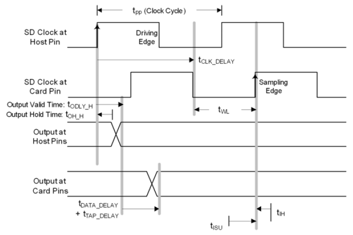
Full-Speed Write Meeting Setup (Maximum Delay)
The following equations show how to calculate the allowed skew range between the SD_CLK and SD_DAT/CMD signals on the PCB.
No clock delay:
With clock delay:
The data can be delayed versus clock up to 5 ns in ideal case of t WL = 20 ns.
Full-Speed Write Meeting Hold (Minimum Delay)
The following equations show how to calculate the allowed skew range between the SD_CLK and SD_DAT/CMD signals on the PCB.
The clock can be delayed versus data up to 18.2 ns (external delay line) in ideal case of t WL = 20 ns, with maximum t TAP_DELAY = 3.2 ns programmed.
Full-Speed Input Path (Read)
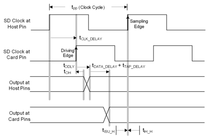
Full-Speed Read Meeting Setup (Maximum Delay)
The following equations show how to calculate the allowed combined propagation delay range of the SD_CLK and SD_DAT/CMD signals on the PCB.
The data + clock delay can be up to 4 ns for a 40 ns clock cycle.
Full-Speed Read Meeting Hold (Minimum Delay)
The following equations show how to calculate the allowed combined propagation delay range of the SD_CLK and SD_DAT/CMD signals on the PCB.
The data + clock delay must be greater than 2 ns if t TAP_DELAY is not used.
If the t TAP_DELAY is programmed to at least 2 ns, the data + clock delay must be greater than 0 ns (or less). This is always fulfilled.
AC Timing Specifications (High-Speed Mode)
Parameter | Symbol | Values | Unit | Note/Test Condition | |
|---|---|---|---|---|---|
Min. | Max. | ||||
Clock frequency in high speed transfer mode (1/ t pp ) | f pp CC | 0 | 48 | MHz | |
Clock cycle in high speed transfer mode | t pp CC | 20 | – | ns | |
Clock low time | t WL CC | 7 | – | ns | |
Clock high time | t WH CC | 7 | – | ns | |
Clock rise time | t TLH CC | – | 3 | ns | |
Clock fall time | t THL CC | – | 3 | ns | |
Inputs setup to clock rising edge | t ISU_H SR | 2 | – | ns | |
Inputs hold after clock rising edge | t IH_H SR | 2 | – | ns | |
Outputs valid time in high speed mode | t ODLY_H CC | – | 14 | ns | |
Outputs hold time in high speed mode | t OH_H CC | 2 | – | ns | |
Parameter | Symbol | Values | Unit | Note/Test Condition | |
|---|---|---|---|---|---|
Min. | Max. | ||||
SD card input setup time | t ISU | 6 | – | ns | |
SD card input hold time | t IH | 2 | – | ns | |
SD card output valid time | t ODLY | – | 14 | ns | |
SD card output hold time | t OH | 2.5 | – | ns | |
High-Speed Output Path (Write)
High-Speed Write Meeting Setup (Maximum Delay)
The following equations show how to calculate the allowed skew range between the SD_CLK and SD_DAT/CMD signals on the PCB.
No clock delay:
With clock delay:
The data delay is less than the clock delay by at least 10 ns in the ideal case where t WL = 10 ns.
High-Speed Write Meeting Hold (Minimum Delay)
The following equations show how to calculate the allowed skew range between the SD_CLK and SD_DAT/CMD signals on the PCB.
The clock can be delayed versus data up to 13.2 ns (external delay line) in ideal case of t WL = 10 ns, with maximum t TAP_DELAY = 3.2 ns programmed.
High-Speed Input Path (Read)
High-Speed Read Meeting Setup (Maximum Delay)
The following equations show how to calculate the allowed combined propagation delay range of the SD_CLK and SD_DAT/CMD signals on the PCB.
The data + clock delay can be up to 4 ns for a 20 ns clock cycle.
High-Speed Read Meeting Hold (Minimum Delay)
The following equations show how to calculate the allowed combined propagation delay range of the SD_CLK and SD_DAT/CMD signals on the PCB.
The data + clock delay must be greater than -0.5 ns for a 20 ns clock cycle. This is always fulfilled.
EBU Timing
Note:
These parameters are not subject to production test, but verified by design and/or characterization.
Note:
Operating Conditions apply, with Class A2 pins and
C L
= 16 pF.
EBU Asynchronous Timing
Note:
For each timing, the accumulated PLL jitter must be added
separately.
Parameter | Symbol | Limit Values | Unit | Edge Setting | |||
|---|---|---|---|---|---|---|---|
Min. | Max. | ||||||
Pulse width deviation from the ideal programmed width due to the A2 pad asymmetry, strong driver mode, rise delay - fall delay. C L = 16 pF. | CC | t a | -1 | 1.5 | ns | sharp | |
-2 | 1 | medium | |||||
AD(24:16) output delay | to rising edge, multiplexed read/write | CC | t 13 | -5.5 | 2 | – | |
AD(24:16) output delay | CC | t 14 | -5.5 | 2 | – | ||
Read Timing
Parameter | Symbol | Limit Values | Unit | |||
|---|---|---|---|---|---|---|
Min. | Max. | |||||
A(24:16) output delay | to rising edge, deviation from the ideal programmed value. | CC | t 0 | -2.5 | 2.5 | ns |
A(24:16) output delay | CC | t 1 | -2.5 | 2.5 | ||
rising edge | CC | t 2 | -2 | 2.5 | ||
rising edge | CC | t 3 | -1.5 | 4.5 | ||
rising edge | CC | t 4 | -2.5 | 2.5 | ||
input setup | SR | t 5 | 12 | – | ||
input hold | SR | t 6 | 0 | – | ||
Data input setup | SR | t 7 | 12 | – | ||
Data input hold | SR | t 8 | 0 | – | ||
RD/ output delay | CC | t 9 | -2.5 | 1.5 | ||
Multiplexed Read Timing
Demultiplexed Read Timing
Write Timing
Parameter | Symbol | Limit Values | Unit | |||
|---|---|---|---|---|---|---|
Min. | Max. | |||||
A(24:0) output delay | to RD/ rising edge, deviation from the ideal programmed value. | CC | t 30 | -2.5 | 2.5 | ns |
A(24:0) output delay | CC | t 31 | -2.5 | 2.5 | ||
rising edge | CC | t 32 | -2 | 2 | ||
rising edge | CC | t 33 | -2 | 4.5 | ||
rising edge | CC | t 34 | -2.5 | 2 | ||
input setup | SR | t 35 | 12 | – | ||
input hold | SR | t 36 | 0 | – | ||
Data output delay | CC | t 37 | -5.5 | 2 | ||
Data output delay | CC | t 38 | -5.5 | 2 | ||
RD/ output delay | CC | t 39 | -2.5 | 1.5 | ||
Multiplexed Write Timing
Demultiplexed Write Timing
EBU Burst Mode Access Timing
Note:
These parameters are not subject to production test, but verified by design and/or characterization.
Note:
Operating Conditions apply, with Class A2 pins and C L = 16 pF.
| Parameter | Symbol | Values | Unit | Note/Test Condition | ||
|---|---|---|---|---|---|---|
| Min. | Typ. | Max. | ||||
| Output delay from BFCLKO rising edge | t 10 CC | -2 | – | 2 | ns | – |
| and RD/ active/inactive after BFCLKO active edge | t 12 CC | -2 | – | 2 | ns | – |
| output delay from BFCLKO active edge 76 | t 21 CC | -2.5 | – | 1.5 | ns | – |
| active/inactive after BFCLKO active edge | t 22 CC | -2 | – | 2 | ns | – |
| active/inactive after BFCLKO active edge 77 | t 22a CC | -2.5 | – | 1.5 | ns | – |
| Data setup to BFCLKI rising edge | t 23 SR | 3 | – | – | ns | – |
| Data hold from BFCLKI rising edge 78 | t 24 SR | 0 | – | – | ns | – |
| setup (low or high) to BFCLKI rising edge 78 | t 25 SR | 3 | – | – | ns | – |
| hold (low or high) from BFCLKI rising edge 78 | t 26 SR | 0 | – | – | ns | – |
EBU Arbitration Signal Timing
Note:
These parameters are not subject to production test, but verified
by design and/or characterization.
Note:
Operating Conditions apply.
Parameter | Symbol | Values | Unit | Note/Test Condition | ||
|---|---|---|---|---|---|---|
Min. | Typ. | Max. | ||||
Output delay from BFCLKO rising edge | t 1 CC | – | – | 16 | ns | C L = 50 pF |
Data setup to BFCLKO falling edge | t 2 SR | 11 | – | – | ns | – |
Data hold from BFCLKO falling edge | t 3 SR | 2 | – | – | ns | – |
EBU SDRAM Access Timing
Note:
These parameters are not subject to production test, but verified
by design and/or characterization.
Note:
Operating Conditions apply, with Class A2 pins and
C L
= 16 pF.
Parameter | Symbol | Values | Unit | Note/Test Condition | ||
|---|---|---|---|---|---|---|
Min. | Typ. | Max. | ||||
SDCLKO period | t 1 CC | 12.5 | – | – | ns | – |
SDCLKO high time | t 2 SR | 5.5 | – | – | ns | – |
SDCLKO low time | t 3 SR | 3.75 | – | – | ns | – |
SDCLKO rise time | t 4 SR | – | – | 3.0 | ns | – |
SDCLKO fall time | t 5 SR | – | – | 3.0 | ns | – |
Parameter | Symbol | Limit Values | Unit | |||
|---|---|---|---|---|---|---|
Min. | Max. | |||||
A(15:0) output valid | from SDCLKO low-to-high transition | CC | t 6 | – | 9 | ns |
A(15:0) output hold | CC | t 7 | 3 | – | ||
low | CC | t 8 | – | 9 | ||
high | CC | t 9 | 3 | – | ||
low | CC | t 10 | – | 9 | ||
high | SR | t 11 | 3 | – | ||
low | SR | t 12 | – | 9 | ||
high | CC | t 13 | 3 | – | ||
RD/ low | CC | t 14 | – | 9 | ||
RD/ high | CC | t 15 | 3 | – | ||
low | CC | t 16 | – | 9 | ||
high | CC | t 17 | 3 | – | ||
D(15:0) output valid | CC | t 18 | – | 9 | ||
D(15:0) output hold | CC | t 19 | 3 | – | ||
CKE output valid | CC | t 22 | – | 7 | ||
CKE output hold 79 | CC | t 23 | 2 | – | ||
D(15:0) input hold | SR | t 21 | 3 | – | ||
D(15:0) input setup to SDCLKO low-to-high transition | SR | t 20 | 4 | – | ||
USB Interface Characteristics
The Universal Serial Bus (USB) Interface is compliant to the USB Rev. 2.0 Specification and the OTG Specification Rev. 1.3. High-Speed Mode is not supported.
Note:
These parameters are not subject to production
test, but verified by design and/or characterization.
Parameter | Symbol | Values | Unit | Note/Test Condition | ||
|---|---|---|---|---|---|---|
Min. | Typ. | Max. | ||||
Rise time | t R CC | 4 | – | 20 | ns | C L = 50 pF |
Fall time | t F CC | 4 | – | 20 | ns | C L = 50 pF |
Rise/Fall time matching | t R / t F CC | 90 | – | 111.11 | % | C L = 50 pF |
Crossover voltage | V CRS CC | 1.3 | – | 2.0 | V | C L = 50 pF |
Ethernet Interface (ETH) Characteristics
For proper operation of the Ethernet Interface it is required that f SYS ≥ 100 MHz.
Note:
These parameters are not subject to production
test, but verified by design and/or characterization.
ETH Measurement Reference Points
ETH Management Signal Parameters (ETH_MDC, ETH_MDIO)
Parameter | Symbol | Values | Unit | Note/Test Condition | ||
|---|---|---|---|---|---|---|
Min. | Typ. | Max. | ||||
ETH_MDC period | t 1 CC | 400 | – | – | ns | C L = 25 pF |
ETH_MDC high time | t 2 CC | 160 | – | – | ns | |
ETH_MDC low time | t 3 CC | 160 | – | – | ns | |
ETH_MDIO setup time (output) | t 4 CC | 10 | – | – | ns | |
ETH_MDIO hold time (output) | t 5 CC | 10 | – | – | ns | |
ETH_MDIO data valid (input) | t 6 SR | 0 | – | 300 | ns | |
ETH MII Parameters
In the following, the parameters of the MII (Media Independent Interface) are described.
Parameter | Symbol | Values | Unit | Note/Test Condition | ||
|---|---|---|---|---|---|---|
Min. | Typ. | Max. | ||||
Clock period, 10 Mbps | t 7 SR | 400 | – | – | ns | C L = 25 pF |
Clock high time, 10 Mbps | t 8 SR | 140 | – | 260 | ns | |
Clock low time, 10 Mbps | t 9 SR | 140 | – | 260 | ns | |
Clock period, 100 Mbps | t 7 SR | 40 | – | – | ns | |
Clock high time, 100 Mbps | t 8 SR | 14 | – | 26 | ns | |
Clock low time, 100 Mbps | t 9 SR | 14 | – | 26 | ns | |
Input setup time | t 10 SR | 10 | – | – | ns | |
Input hold time | t 11 SR | 10 | – | – | ns | |
Output valid time | t 12 CC | 0 | – | 25 | ns | |
ETH RMII Parameters
In the following, the parameters of the RMII (Reduced Media Independent Interface) are described.
Parameter | Symbol | Values | Unit | Note/Test Condition | ||
|---|---|---|---|---|---|---|
Min. | Typ. | Max. | ||||
ETH_RMII_REF_CL clock period | t 13 SR | 20 | – | – | ns | C L = 25 pF; 50 ppm |
ETH_RMII_REF_CL clock high time | t 14 SR | 7 | – | 13 | ns | C L = 25 pF |
ETH_RMII_REF_CL clock low time | t 15 SR | 7 | – | 13 | ns | |
ETH_RMII_RXD[1:0], ETH_RMII_CRS setup time | t 16 SR | 4 | – | – | ns | |
ETH_RMII_RXD[1:0], ETH_RMII_CRS hold time | t 17 SR | 2 | – | – | ns | |
ETH_RMII_TXD[1:0], ETH_RMII_TXEN data valid | t 18 CC | 4 | – | 15 | ns | |
Package and Reliability
The XMC4500 is a member of the XMC4000 Family of microcontrollers. It is also compatible to a certain extent with members of similar families or subfamilies.
Each package is optimized for the device it houses. Therefore, there may be slight differences between packages of the same pin-count but for different device types. In particular, the size of the Exposed Die Pad may vary.
If different device types are considered or planned for an application, it must be ensured that the board layout fits all packages under consideration.
Package Parameters
Table 64 provides the thermal characteristics of the packages used in XMC4500.
Parameter | Symbol | Limit Values | Unit | Package Types | |
|---|---|---|---|---|---|
Min. | Max. | ||||
Exposed Die Pad dimensions (including U-Groove where applicable) | Ex × Ey CC | – | 6.5 × 6.5 | mm | PG-LQFP-144-24 |
– | 7.0 × 7.0 | mm | PG-LQFP-100-25 | ||
Exposed Die Pad dimensions | – | – | 7.0 × 7.0 | mm | PG-LQFP-100-29 |
– | – | 6.5 × 6.5 | mm | PG-LQFP-144-26 | |
Thermal resistance Junction-Ambient T J ≤ 150°C | R ΘJA CC | – | 40.5 | K/W | PG-LFBGA-144-10 |
– | 19.5 | K/W | PG-LQFP-144-24 | ||
– | 21.0 | K/W | PG-LQFP-100-25 80 | ||
– | 21.0 | K/W | PG-LQFP-100-29 80 | ||
– | 19.5 | K/W | PG-LQFP-144-26 80 | ||
Note:
For electrical reasons, it is required to connect
the exposed pad to the board ground
V SS
, independent of EMC and thermal requirements.
Thermal Considerations
When operating the XMC4500 in a system, the total heat generated in the chip must be dissipated to the ambient environment to prevent overheating and the resulting thermal damage.
The maximum heat that can be dissipated depends on the package and its integration into the target board. The “Thermal resistance R ΘJA ” quantifies these parameters. The power dissipation must be limited so that the average junction temperature does not exceed 150°C.
The difference between junction temperature and ambient temperature is determined by
Δ T = ( P INT + P IOSTAT + P IODYN ) × R ΘJA
The internal power consumption is defined as
P INT = V DDP × I DDP (switching current and leakage current).
The static external power consumption caused by the output drivers is defined as
P IOSTAT = Σ(( V DDP - V OH ) × I OH ) + Σ( V OL × I OL )
The dynamic external power consumption caused by the output drivers ( P IODYN ) depends on the capacitive load connected to the respective pins and their switching frequencies.
If the total power dissipation for a given system configuration exceeds the defined limit, countermeasures must be taken to ensure proper system operation:
Reduce V DDP , if possible in the system
Reduce the system frequency
Reduce the number of output pins
Reduce the load on active output drivers
Package Outlines
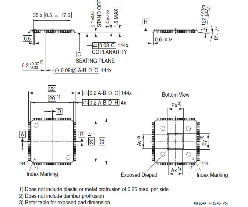
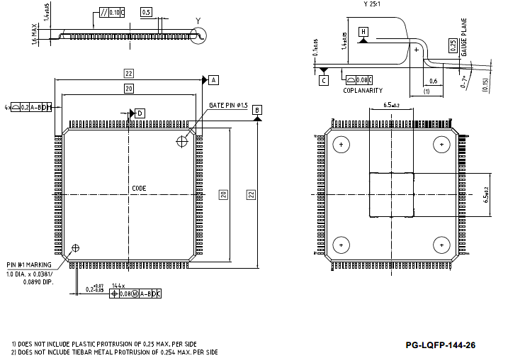
Figure 59. PG-LFBGA-144-10 (Plastic Green Low Profile Fine Pitch Ball Grid Array)
All dimensions in mm.
You can find complete information about Infineon packages, packing and marking in our Infineon Internet Page “Packages”: http://www.infineon.com/packages .
Quality Declarations
The qualification of the XMC4500 is executed according to the JEDEC standard JESD47H.
Note:
For automotive applications refer to the Infineon automotive
microcontrollers.
Parameter | Symbol | Values | Unit | Note/Test Condition | ||
|---|---|---|---|---|---|---|
Min. | Typ. | Max. | ||||
Operation lifetime | t OP CC | 20 | – | – | a | T J ≤ 109°C, device permanent on |
ESD susceptibility according to Human Body Model (HBM) | V HBM SR | – | – | 2000 | V | EIA/JESD22-A114-B |
ESD susceptibility according to Charged Device Model (CDM) | V CDM SR | – | – | 500 | V | Conforming to JESD22-C101-C |
Moisture sensitivity level | MSL CC | – | – | 3 | – | JEDEC J-STD-020D |
Soldering temperature | T SDR SR | – | – | 260 | °C | Profile according to JEDEC J-STD-020D |
Revision history
Document revision | Date | Description of changes |
|---|---|---|
V1.6 | 2023-04-01 | Table 64 : Added package details: PG-LQFP-100-29 and PG-LQFP-144-26. Deleted package details: PG-LQFP-100-11 and PG-LQFP-144-18. Added package diagrams: PG-LQFP-100-29 and PG-LQFP-144-26. Deleted package diagrams: PG-LQFP-100-11 and PG-LQFP-144-18. |
V1.7 | 2024-12-02 | Template update; no content update |
1
x is a placeholder for the supported temperature range.
2
x is a placeholder for the supported temperature range.
3
Memory types supported S=SDRAM, D=DEMUX, M=MUX 16-bit and 32-bit, M16=MUX 16-bit.
4
Supported interfaces, M=MII, R=RMII.
5
x is a placeholder for the supported temperature range.
6
Some pins in a package may be connected to more than one channel. For the detailed mapping see the Port I/O Function table.
10
Voltage overshoot to 4.0 V is permissible at Power-Up and
low, provided the pulse duration is less than 100 μs and the cumulated sum of the pulses does not exceed 1 h over lifetime.
11
To start the hibernate domain it is required that V BAT ≥ 2.1 V, for a reliable start of the oscillation of RTC_XTAL in crystal mode it is required that V BAT ≥ 3.0 V.
13
Current required to override the pull device with the opposite logic level (“force current”). With active pull device, at load currents between force and keep current the input state is undefined.
14
Load current at which the pull device still maintains the valid logic level (“keep current”). With active pull device, at load currents between force and keep current the input state is undefined.
15
Hysteresis is implemented to avoid metastable states and switching due to internal ground bounce. It can not be guaranteed that it suppresses switching due to external system noise.
16
POD = Pin Out Driver.
17
POD = Pin Out Driver.
18
Applies to AINx, when used as alternate reference input.
19
A running conversion may become imprecise in case the normal conditions are violated (voltage overshoot).
20
If the analog reference voltage is below VDDA, then the ADC converter errors increase. If the reference voltage is reduced by the factor k (k<1), TUE, DNL, INL, Gain, and Offset errors increase also by the factor 1/k.
21
The leakage current definition is a continuous function, as shown in figure ADCx Analog Inputs Leakage. The numerical values defined determine the characteristic points of the given continuous linear approximation - they do not define step function (see
Figure 16
).
22
The sampling capacity of the conversion C-network is pre-charged to V AREF /2 before the sampling moment. Because of the parasitic elements, the voltage measured at AINx can deviate from V AREF /2.
23
This represents an equivalent switched capacitance. This capacitance is not switched to the reference voltage at once. Instead, smaller capacitances are successively switched to the reference voltage.
24
For 10-bit conversions, the errors are reduced to 1/4; for 8-bit conversions, the errors are reduced to 1/16. Never less than ±1 LSB.
25
The sum of DNL/INL/GAIN/OFF errors does not exceed the related total unadjusted error TUE.
26
This parameter is valid for soldered devices and requires careful analog board design.
27
Resulting worst case combined error is arithmetic combination of TUE and EN RMS .
28
Value is defined for one sigma Gauss distribution.
29
The resulting current for a conversion can be calculated with I AREF = Q CONV / t c. The fastest 12-bit post-calibrated conversion of t c = 550 ns results in a typical average current of I AREF = 54.5 μA.
30
Always the standard VADC reference, alternate references do not apply to the ORC.
31
At V DDP_max = 3.63 V the typical offset error increases by an additional Δ T OE = ±1°C.
32
Measured at A-connector with 1.5 kOhm ± 5% to 3.3 V ± 0.3 V connected to USB_DP or USB_DM and at B-connector with 15 kOhm ± 5% to ground connected to USB_DP and USB_DM.
33
t OSCS is defined from the moment the oscillator is enabled wih SCU_OSCHPCTRL.MODE until the oscillations reach an amplitude at XTAL1 of 0.4 * V DDP .
34
The external oscillator circuitry must be optimized by the customer and checked for negative resistance and amplitude as recommended and specified by crystal suppliers.
35
If the shaper unit is enabled and not bypassed.
36
If the shaper unit is bypassed, dedicated DC-thresholds have to be met.
37
t OSCS is defined from the moment the oscillator is enabled by the user with SCU_OSCULCTRL.MODE until the oscillations reach an amplitude at RTC_XTAL1 of 400 mV.
38
The external oscillator circuitry must be optimized by the customer and checked for negative resistance and amplitude as recommended and specified by crystal suppliers.
39
For a reliable start of the oscillation in crystal mode it is required that V BAT ≥ 3.0 V. A running oscillation is maintained across the full V BAT voltage range.
40
If the shaper unit is enabled and not bypassed.
41
If the shaper unit is bypassed, dedicated DC-thresholds have to be met.
42
Hysteresis is implemented to avoid metastable states and switching due to internal ground bounce. It can not be guaranteed that it suppresses switching due to external system noise.
43
CPU executing code from Flash, all peripherals idle.
44
Test Power Loop: f SYS = 120 MHz, CPU executing benchmark code from Flash, all CCUs in 100 kHz timer mode, all ADC groups in continuous conversion mode, USICs as SPI in internal loop-back mode, CAN in 500 kHz internal loop-back mode, interrupt triggered DMA block transfers to parity protected RAMs and FCE, DTS measurements and FPU calculations.
The power consumption of each customer application will most probably be lower than this value, but must be evaluated separately.
45
CPU executing code from Flash.
46
CPU in sleep, all peripherals idle, Flash in Active mode.
47
CPU in sleep, Flash in Active mode.
48
CPU in sleep, peripherals disabled, after wake-up code execution from RAM.
49
To wake-up the Flash from its Sleep mode, f CPU ≥ 1 MHz is required.
50
OSC_ULP operating with external crystal on RTC_XTAL.
51
OSC_ULP off, Hibernate domain operating with OSC_SI clock.
52
I DDP decreases typically by approximately 6 mA when f SYS decreases by 10 MHz, at constant T J
53
Sum of currents of all active converters (ADC and DAC).
54
In case the Program Verify feature detects weak bits, these bits will be programmed once more. The reprogramming takes an additional time of 5.5 ms.
55
The following formula applies to the wait state configuration: FCON.WSPFLASH × (1/ f CPU ) ≥ t a .
56
Storage and inactive time included.
57
Values given are valid for an average weighted junction temperature of T J = 110°C.
58
Minimum threshold for reset assertion.
59
Maximum threshold for reset deassertion.
60
The V DDP monitoring has a typical hysteresis of V PORHYS = 180 mV.
61
If t PR is not met, low spikes on
may be seen during start up (e.g. reset pulses generated by the supply monitoring due to a slow ramping V DDP ).
62
50% for even K2 divider values, 50±(10/K2) for odd K2 divider values.
63
Error in addition to the accuracy of the reference clock.
64
Automatic calibration compensates variations of the temperature and in the V DDP supply voltage.
65
Deviations from the nominal V DDP voltage induce an additional error to the uncalibrated and/or factory calibrated oscillator frequency.
66
The falling edge on TCK is used to generate the TDO timing.
67
The setup time for TDO is given implicitly by the TCK cycle time.
68
t PERIPH = 1/ f PERIPH
69
t PB = 1/ f PB
70
This input timing is valid for asynchronous input signal handling of slave select input, shift clock input, and receive data input (bits DXnCR.DSEN = 0).
71
Due to the wired-AND configuration of an IIC bus system, the port drivers of the SCL and SDA signal lines need to operate in open-drain mode. The high level on these lines must be held by an external pull-up device, approximately 10 kOhm for operation at 100 kbit/s, approximately 2 kOhm for operation at 400 kbit/s.
72
Due to the wired-AND configuration of an IIC bus system, the port drivers of the SCL and SDA signal lines need to operate in open-drain mode. The high level on these lines must be held by an external pull-up device, approximately 10 kOhm for operation at 100 kbit/s, approximately 2 kOhm for operation at 400 kbit/s.
73
C b refers to the total capacitance of one bus line in pF.
74
Reference card timing values for calculation examples. Not subject to production test and not characterized.
75
Reference card timing values for calculation examples. Not subject to production test and not characterized.
76
An active edge can be a rising or falling edge, depending on the settings of bits BFCON.EBSE/ECSE and the clock divider ratio.
Negative minimum values for these parameters mean that the last data read during a burst may be corrupted. However, with clock feedback enabled, this value is an oversampling not required for the internal bus transaction, and will be discarded.
77
This parameter is valid for BUSCONx.EBSE = 1 and BUSAPx.EXTCLK = 00 .
For BUSCONx.EBSE = 1 and other values of BUSAPx.EXTCLK, ADV and BAA will be delayed by 1/2 of the internal bus clock period T CPU = 1/ f CPU .
For BUSCONx. EBSE = 0 and BUSAPx.EXTCLK = 11 , add 2 internal bus clock periods.
For BUSCONx. EBSE = 0 and other values of BUSAPx.EXTCLK, add 1 internal bus clock period.
78
If the clock feedback is not enabled, the input signals are latched using the internal clock in the same way as for asynchronous access. Thus, t 5 , t 6 , t 7 and t 8 from the asynchronous timing apply.
79
Not depicted in the read and write access timing figures below.
80
Device mounted on a 4-layer JEDEC board (JESD 51-7) with thermal vias; exposed pad soldered.